The advertised number is the wrong number
Almost the entire public vocabulary for AI hardware is arithmetic: petaflops, TOPS, “compute”. It is a vocabulary that describes the least binding half of the machine. A modern accelerator has more arithmetic capability than it can keep fed for most of the work actually asked of it, and the parts of the design that took the real engineering effort — the stacked memory, the interposer under the die, the on-chip staging buffers, the links to the next chip — exist to narrow that gap rather than to widen the arithmetic.
The thesis of this article is that an AI accelerator is best understood as a memory system with arithmetic attached, and that every serious design decision of the last decade follows from that reading. The evidence is not rhetorical. Gholami and colleagues measured the divergence directly and reported that peak server hardware FLOPS has been scaling at roughly 3.0x every two years while DRAM bandwidth scales at about 1.6x and interconnect bandwidth at about 1.4x over the same interval [4]. Two decades of that compounding produces a machine whose arithmetic units are, for a large class of workloads, idle waiting on bytes.
That is not a defect. It is a design point, and it is the correct one — arithmetic is cheap in area and energy relative to moving the operands to it. But it means that reasoning about these machines from their headline arithmetic is reasoning from the wrong end. What follows works from the memory outward: what the arithmetic array is for, what governs whether it can be used, why the memory was physically relocated, and what happens when one die is not enough.
The matrix unit, and the reuse that justifies it
Neural network training and inference are dominated by dense matrix multiplication. That single fact is what made a domain-specific accelerator worth building, because dense matrix multiplication has an unusual property: the amount of arithmetic it performs grows faster than the amount of data it consumes.
Multiplying an
which for large square matrices grows in proportion to the dimension. Double the matrix size and you roughly double the work performed per byte fetched. Almost nothing else in general-purpose computing behaves this way, and it is the entire economic basis for building a machine around one operation.
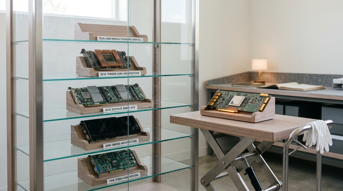
The architectural response is a two-dimensional array of multiply-accumulate units through which operands are pumped so that each value fetched once from memory is used many times as it propagates across the array. Google’s first Tensor Processing Unit is the clearest documented instance: the ISCA 2017 paper describes a 65,536 8-bit multiply-accumulate matrix unit with a large 28 MiB software-managed on-chip memory and a peak throughput of 92 TeraOps per second [1]. The proportions are the point. Tens of thousands of arithmetic units are cheap enough to spend freely; the scarce, expensive, carefully managed resource is the on-chip buffer that keeps them supplied, and the paper’s authors chose to make it software-managed rather than a cache precisely so that the reuse pattern could be scheduled rather than hoped for.
Later generations kept the shape while changing everything around it. The TPU v4 paper reports its chips deployed in 4,096-chip systems whose interconnect topology is dynamically reconfigured by optical circuit switches, and its authors state that TPU v4 outperforms TPU v3 by 2.1x with a 2.7x improvement in performance per watt [3]. Those are the designers’ own reported figures for successive generations of one product line, which is the only kind of speedup comparison that means anything; they are not a claim about any other vendor’s parts.
The commodity GPU converged on the same structure from the other direction, adding matrix-multiply units alongside its general vector pipelines and then adding machinery whose sole purpose is feeding them. NVIDIA’s Hopper documentation describes a Tensor Memory Accelerator, an asynchronous copy engine for moving tensors between memory spaces, and records shared memory capacity rising to 228 KB per streaming multiprocessor against 164 KB in the previous generation, with L2 cache growing from 40 MB to 50 MB [10]. Read that list again: an engine for moving data, a bigger staging buffer, a bigger cache. The generational change most visible in the tuning guide is not arithmetic.
The roofline: one model that governs everything else
There is a single analysis that organises all of this, and anyone reasoning about accelerators without it is guessing. Williams, Waterman and Patterson proposed the roofline model as a visual performance bound relating a machine’s peak arithmetic rate to its memory bandwidth through a program’s operational intensity [2].
Define arithmetic intensity
with
That expression is the whole model, and it has one structural feature that matters more than the rest. The two bounds cross at a ridge point
the arithmetic intensity a workload must exceed before the machine’s peak rate is even theoretically reachable. Below
Now put the two scaling rates from the opening beside this. If

The model also explains why kernel engineering has taken the shape it has. FlashAttention is the canonical demonstration: Dao and colleagues argued that attention implementations were missing an IO-aware principle, and used tiling to reduce reads and writes between high-bandwidth memory and on-chip SRAM, reporting speedups including 3x on GPT-2 at sequence length 1K and 15% end-to-end on BERT-large at sequence length 512 [5]. The arithmetic performed did not fall — the result is exact attention, not an approximation. What fell was
Why the memory was moved next to the die
If
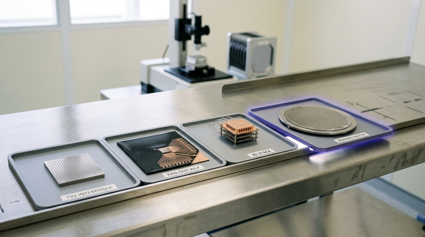
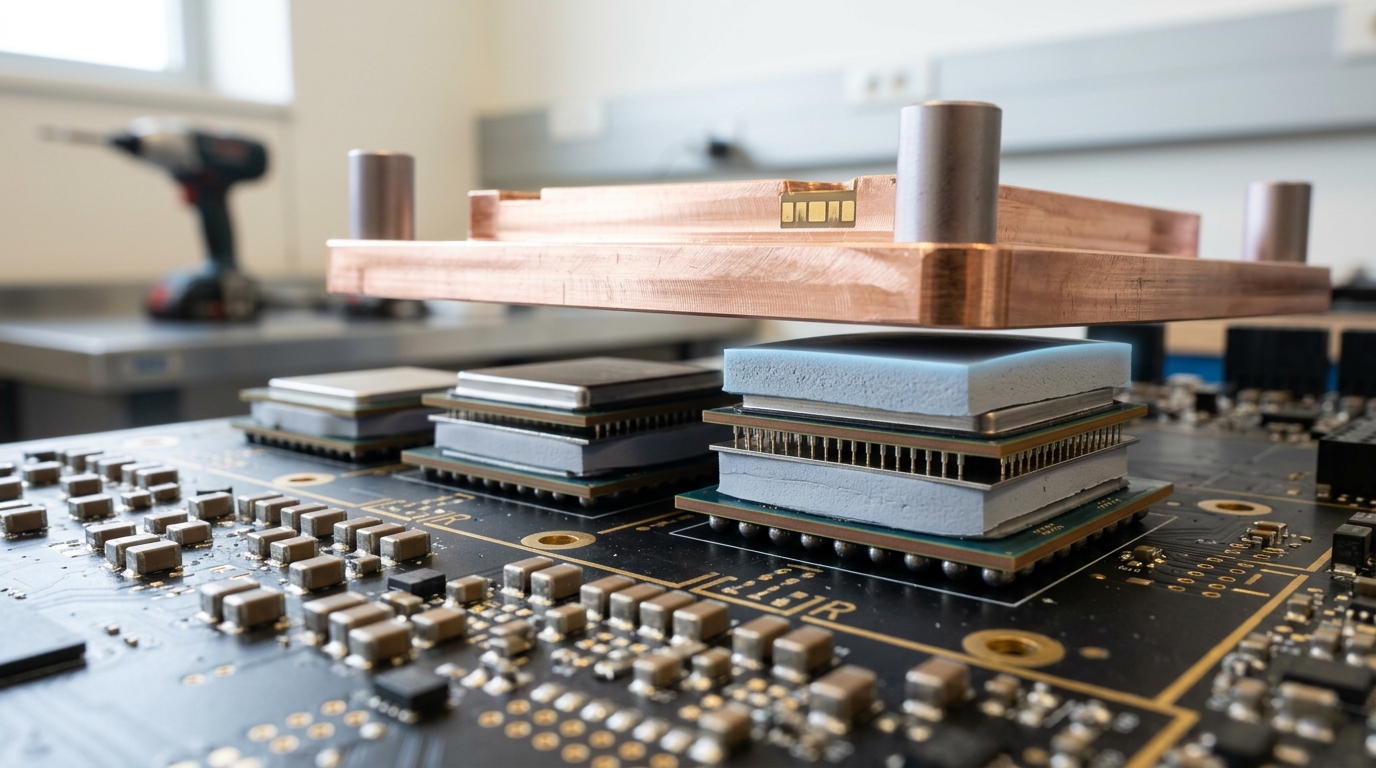
High-bandwidth memory takes the other branch. DRAM dies are stacked vertically and connected by through-silicon vias into a single cube, and that cube is placed on a silicon interposer immediately beside the processor die, so the memory interface becomes extremely wide and extremely short. The trade is width for distance: thousands of parallel connections running millimetres instead of hundreds running centimetres. The consequence is a step change in
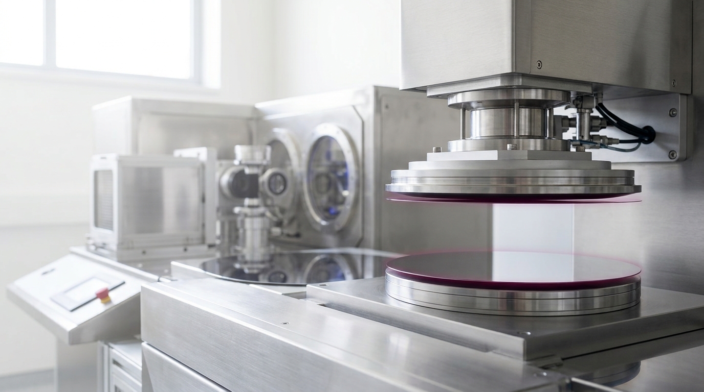
This is what advanced packaging is for. TSMC describes its 3DFabric portfolio — comprising SoIC, CoWoS and InFO — as letting customers design products “as a system of mini-chips that offers key advantages versus designing a larger monolithic die,” and offers it as an integrated service specifically because chip-package integration issues cross the old boundary between silicon and packaging [12]. That vendor framing is worth taking literally rather than as marketing. Packaging stopped being the step after the chip was finished and became a co-designed part of the chip, because the memory interface is now inside the package.
The magnitude is visible in vendor specifications. NVIDIA states that its H100 SXM5 was the first GPU with HBM3 memory, delivering 3 TB/s of memory bandwidth, and that the underlying GH100 die is fabricated on a TSMC 4N process with 80 billion transistors [9]. Both figures are the vendor’s own disclosures about its own part and should be read that way. The relevant observation is not the number but the ratio it implies: a device with that much arithmetic still needs terabytes per second of adjacent memory to keep it occupied, and the industry was willing to invent a new packaging discipline to supply it.
Two consequences follow that buyers routinely miss. First, capacity and bandwidth are now coupled through the same physical mechanism, so a part cannot easily be specified with a lot of one and little of the other. Second, packaging capacity, not wafer capacity, becomes a supply constraint for accelerators — because the interposer step is a separate manufacturing flow with its own throughput.

Peak, achieved, and bandwidth-limited are three different numbers
Three quantities circulate under the single word “performance”, and conflating them is the most common error in procurement.
Peak FLOPS is an arithmetic identity: functional units multiplied by operations per unit per cycle multiplied by clock frequency. It is exactly computable, never achievable, and tells you
Achieved FLOPS is what a specific kernel attains on specific data on a specific software stack. The gap to peak comes from instruction issue, memory stalls, tail effects on the last tile of a matrix, synchronisation, and clock behaviour under sustained load.
Bandwidth-limited throughput is the regime where achieved FLOPS is irrelevant because
a floor set entirely by memory traffic, in which peak arithmetic does not appear. This is why batching improves throughput so dramatically — the same weight bytes are amortised across many sequences, raising
The TPU paper contains a striking demonstration of exactly this asymmetry from the hardware side. Its authors reported that simply substituting the contemporary GPU’s memory for the TPU’s own would have tripled achieved TOPS on their workloads, with no change whatsoever to the arithmetic array [1]. A three-fold performance change from a memory swap is not a footnote about one 2015-era part. It is the thesis of this article stated as a measurement.
When one die is not enough
Frontier models exceed any single device, so the accelerator’s boundary is not the package. It is the interconnect, and the operations that run across it are collectives rather than point-to-point messages.
The library interface makes the vocabulary explicit: NCCL documents AllReduce, Broadcast, Reduce, AllGather, ReduceScatter, AllToAll, Gather and Scatter, alongside point-to-point send and receive [11]. Data-parallel training is built on AllReduce over gradients; tensor parallelism inserts AllReduce or ReduceScatter inside every layer’s forward and backward pass; expert-parallel mixture-of-experts routing is an AllToAll. These are not incidental. They are on the critical path of every step.
Their cost has a shape worth internalising. For the standard ring formulation of an all-reduce over
with
NVIDIA states that fourth-generation NVLink operates at 900 GB/s of total bandwidth per H100 for multi-GPU IO [9]. Set that against the same vendor’s 3 TB/s figure for local memory on the same part and the hierarchy is plain: leaving the package costs roughly an order of magnitude in bandwidth, and leaving the node costs more again. Parallelism strategy is the art of arranging for the largest data movements to stay on the fastest tier.
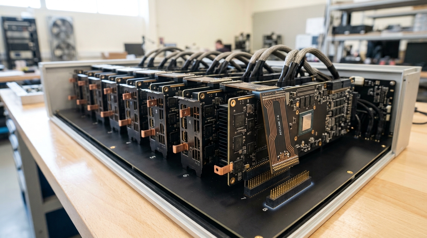
Topology is a first-class design variable at this level, not a deployment detail. The TPU v4 authors report using optical circuit switches to reconfigure the interconnect topology dynamically, and state that the optical components account for less than 5% of system cost and less than 3% of system power [3]. That is a disclosed design claim about their own system. Its general lesson is that at supercomputer scale the network is cheap relative to what topology mismatch costs in idle accelerators.
Precision is a bandwidth decision wearing numerical clothes
Reducing numerical precision is usually presented as a way to get more arithmetic. Its more important effect is halving the bytes, which moves a workload rightward along the intensity axis and relieves both memory and interconnect pressure simultaneously.
The technique’s foundation is well documented. Micikevicius and colleagues established mixed-precision training: store weights, activations and gradients in IEEE half precision, keep a single-precision master copy of the weights for accumulation, and scale the loss so that small gradient values survive the narrower exponent range — reporting close to a 2x reduction in memory consumption across convolutional, recurrent and generative architectures [6]. Note the structure of the fix. Precision was not reduced uniformly; it was reduced where the data volume is and preserved where the numerics are fragile.
The 8-bit generation follows the same logic with two formats rather than one. The FP8 proposal specifies E4M3 with a 4-bit exponent and 3-bit mantissa and E5M2 with a 5-bit exponent and 2-bit mantissa, and its authors report matching 16-bit result quality across convolutional, recurrent and transformer models up to 175 billion parameters without changing hyperparameters from the 16-bit baseline [7]. Two formats exist because gradients need dynamic range while activations and weights need mantissa bits, and a single 8-bit encoding cannot serve both.
Below 8 bits the answer has been block scaling. Microscaling formats pair a per-block scaling factor with narrow floating-point or integer element types, and the authors report evaluations across two dozen benchmarks as a drop-in replacement for FP32 in inference and training, including what they describe as the first instance of training generative language models at sub-8-bit weights, activations and gradients with minimal accuracy loss and no modification to the training recipe [8]. The mechanism is worth naming plainly: a shared exponent amortised over a small block recovers most of the dynamic range that the narrow element type gave up, at a modest cost in bits per element.
What reduced precision costs is real and is usually misstated. It is not primarily accuracy — the results above indicate accuracy can largely be held. It is numerical fragility and evaluation burden: narrower formats have less headroom before overflow or underflow, outlier-heavy tensors behave badly, results become sensitive to accumulation order and to where the master copy is kept, and every reduction in width demands its own validation on the specific model. A vendor’s peak throughput figure at the narrowest supported format is therefore the least transferable number on a datasheet, since it presumes a numerical regime the buyer’s workload may not tolerate.
The node name, separated from the node
One last layer of confusion sits underneath all of this. Process-node labels — the nanometre numbers — have not denoted a physical feature dimension for decades. IEEE Spectrum’s account quotes the observation that the industry’s node number “had by then absolutely no meaning, because it had nothing to do with any dimension that you can find on the die,” and describes researchers proposing an LMC metric combining logic, memory and connectivity densities as a more meaningful measure of progress [13].
Two practical rules follow. First, node names are comparable only within a single foundry’s own sequence, and even then imperfectly; comparing one company’s number to another’s is comparing marketing conventions. Second, the disclosures that carry information are the physical ones — transistor count, die area, and the packaging configuration. NVIDIA’s statement that GH100 uses a TSMC 4N process with 80 billion transistors is informative because of the second clause, not the first [9].
There is a deeper reason the node has become a weaker predictor. When a large fraction of a product’s capability comes from stacked memory beside the die and from what the package integrates, the transistors’ feature size is only one input among several. A vendor’s own framing of packaging as a way to compose systems from mini-chips rather than scale a monolithic die is an admission that the node alone no longer carries the roadmap [12].
Reading a datasheet, and four predictions
The measurement discipline that follows from the roofline is short.
Ask for the ridge point, not the peak.
State the precision with every throughput figure. A peak quoted at the narrowest supported format is not comparable to one quoted at a format you have validated.
Separate local bandwidth from link bandwidth. They differ by roughly an order of magnitude on current parts and they bind different phases of the work.
Never build cross-vendor rankings from vendor-reported speedups. Generational claims are made against the vendor’s own prior part under the vendor’s own measurement conditions and do not compose across companies.
Four predictions follow, clearly separated from the sourced analysis above. Horizon: 8 August 2029.
One. The ratio of peak arithmetic to memory bandwidth will continue to rise across successive generations, so a larger fraction of shipped kernels will be memory bound at introduction than at the previous generation’s introduction. Disconfirmed if published specifications show bandwidth growth matching or exceeding arithmetic growth over two consecutive generations from any major vendor.
Two. Advanced packaging capacity, not leading-edge wafer capacity, will remain the reported constraint on accelerator supply. Disconfirmed if supply commentary shifts decisively to front-end wafer starts while packaging capacity is reported as slack.
Three. Block-scaled sub-8-bit formats will become the default training numerics for frontier-scale models rather than a research option, because the bandwidth relief compounds across memory and interconnect simultaneously. Disconfirmed if the major training stacks still default to 16-bit or unscaled 8-bit element types in 2029.
Four. Interconnect topology and collective scheduling will account for a larger share of published end-to-end training speedups than arithmetic improvements. Disconfirmed if generational training-throughput gains are attributed chiefly to arithmetic units in vendor and academic post-mortems.
None of these requires a discontinuity. They are extrapolations of a ratio that has been moving in one direction for twenty years [4].
What to take away
An engraved plate can hold detail far finer than anything the press will ever exploit in an hour of printing, because the rate at which prints come off is set by the roller, the felt, and how quickly damp paper can be brought to the bed. The plate is the arithmetic. The press and the paper stock are the memory system. Improving the engraving does not shorten the edition.
An AI accelerator is a memory system with arithmetic attached. The matrix unit exists because dense linear algebra is the one operation whose work grows faster than its data. The roofline tells you whether that unit can be used at all, and its ridge point rises with every generation. High-bandwidth memory and the packaging that holds it exist to keep the ridge point reachable. Collectives are where the same argument reappears one level up, with an order of magnitude less bandwidth to work with. Reduced precision is bandwidth relief before it is arithmetic. And the node name on the box is the least informative fact available about any of it.
Ask what the machine can reach, how fast, and from how far away. Everything else on the datasheet is downstream of those three answers.