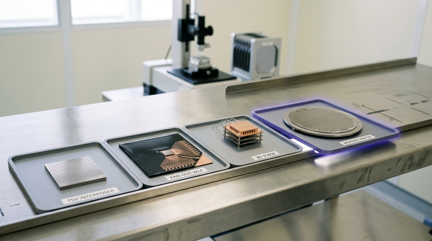
Four ways to leave one piece of silicon
Once a design has been cut into more than one die, something has to join the pieces back into a working system, and there is no single accepted way to do it. Four approaches are in volume production today, side by side, for different products from different vendors: 2.5D integration, which sets dies next to each other on a silicon interposer with a dense field of routing beneath them; fan-out wafer-level packaging, which embeds dies in a reconstituted panel and routes between them in a redistribution layer with no interposer at all; 3D stacking, which puts one die directly on top of another and connects them vertically through microbumps; and hybrid bonding, which removes the bump entirely and joins two flattened, copper-patterned surfaces face to face.
These are not four points on one quality ladder, and treating them as such is the most common mistake in casual comparisons of the field. Each solves the same underlying problem — moving a signal from one piece of silicon to another without paying the cost of a long board-level trace — but each pays a different specific price to do it, and the price is not measured on a common scale. A silicon interposer is expensive because it is a whole extra piece of processed silicon. A fan-out panel is warpage-prone because it is a slab of dissimilar materials cured together. A 3D stack is thermally constrained because heat has only one face to leave through. A hybrid-bonded joint is defect-intolerant because there is no solder left to absorb a stray particle or a few nanometres of surface unevenness. None of these costs converts cleanly into any of the others, which is exactly why no single number can rank the four approaches and why real design teams routinely use more than one of them in the same product.
This article works through each approach in turn, on its own physical terms, then reads the four back against the specific axes a packaging decision actually turns on: bandwidth density per unit of joint area, cost, thermal headroom, and yield risk. It closes by naming where informed opinion in the field genuinely diverges, because on at least two live questions it does, and neither is close to settled.
Topology and joining method are two different choices
Before comparing the four approaches it is worth being precise about what “hybrid bonding” actually is, because a casual reading of the last few years of coverage can leave the impression that it is a fifth, more advanced tier sitting above 2.5D, fan-out, and 3D stacking. It is not. Hybrid bonding is a joining method — direct copper-to-copper and dielectric-to-dielectric bonding between two flattened surfaces, with no bump, no solder, and no reflow step. It can be, and increasingly is, used to build a 3D stack: two dies bonded face to face are still a 3D stack, just one joined by direct bonding instead of by microbumps. The UCIe consortium’s own specification family reflects this directly, describing UCIe-3D as “optimized for hybrid bonding” at bump pitches “as big as 10-25 microns to as small as 1 micron or less,” explicitly as a variant of 3D packaging rather than a separate topology [1].
So the honest way to hold four things in mind at once is as two independent choices. The first choice is topology: do the dies sit next to each other on a shared lateral carrier (2.5D and fan-out), or on top of each other (3D)? The second choice is joining method: are the connections made through discrete bumps that are reflowed, or through a direct, bumpless bond between prepared surfaces? Microbump 3D stacking and hybrid-bonded 3D stacking are the same topology with two different joining methods; 2.5D and fan-out are the same topology — lateral — with two different ways of building the routing layer beneath the dies, one using a monolithic piece of silicon and one using a molded, reconstituted panel. Comparing all four as if they were mutually exclusive rungs on one ladder obscures this, so the sections below keep the distinction explicit throughout.
2.5D: side by side on a piece of silicon built for the job
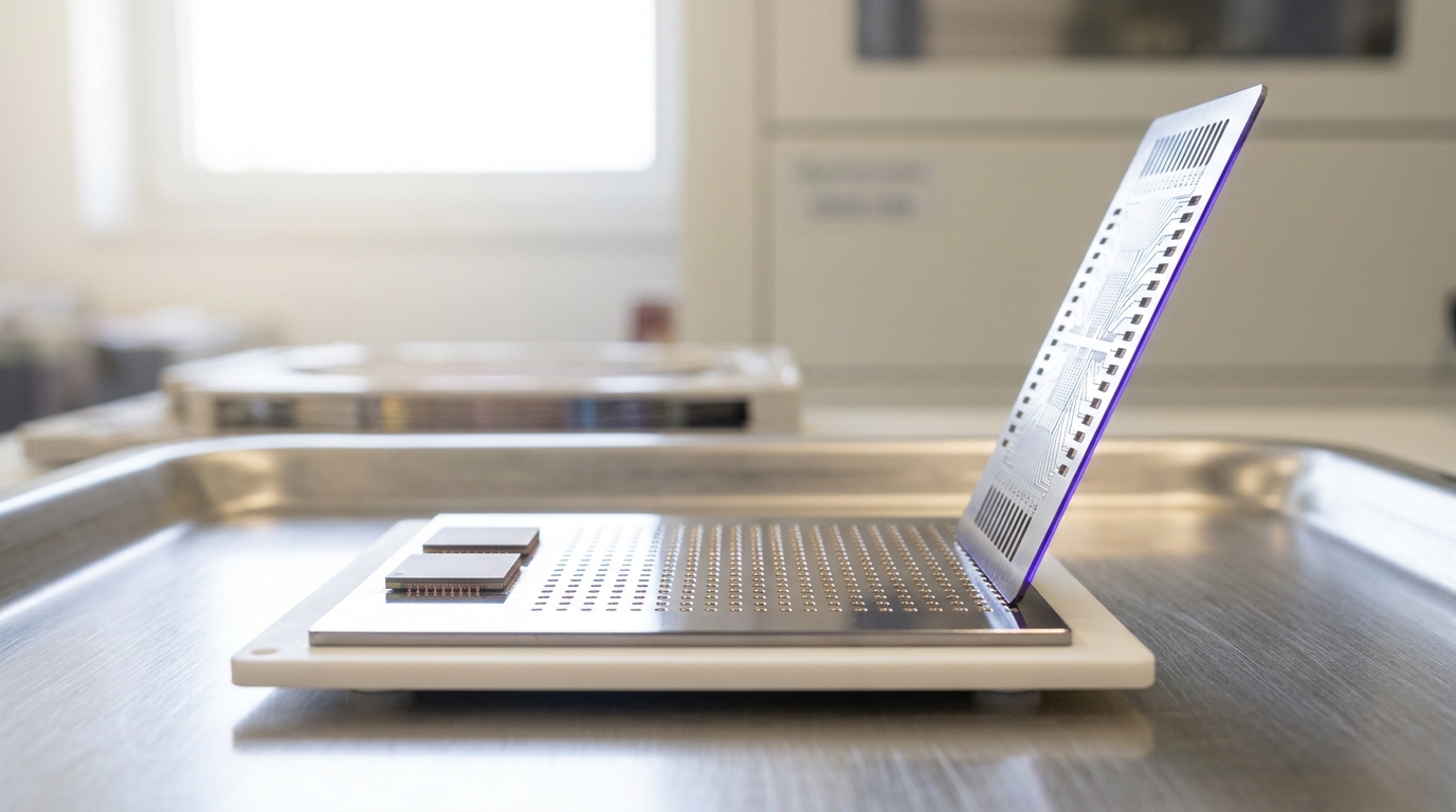
In 2.5D integration, two or more dies sit side by side on a silicon interposer — a passive piece of silicon carrying no active transistors, only a dense field of routing and through-silicon vias (TSVs) that carry signals down to the package substrate beneath it. TSMC’s own documentation for its CoWoS platform describes it as a “wafer level system integration platform” providing “best-in-breed performance and highest integration density for high performance computing applications,” built around silicon interposers combined with TSVs for “exceptional signal and power integrity” [3]. The dies never touch each other directly; every signal between them crosses the interposer’s routing, which can be built at geometries finer than any organic substrate can match.
That routing density is the whole point. imec’s account of the packaging landscape places interposer routing well ahead of the alternatives on pitch: “interposers still hold first place with submicron pitches,” while comparable redistribution-layer routing on other platforms is only reaching toward two-micrometre pitches “and even submicron further down the road” [6]. Fine routing directly buys bandwidth, and TSMC’s own published product examples make the scale concrete: a 2019-era seven-nanometre GPU shipped with four HBM2 stacks on a standard-reticle interposer at 1 terabyte per second of memory bandwidth, and an AI training accelerator on a 1.5x-reticle interposer reached 1.2 terabytes per second with the same stack count [3]. The largest interposers TSMC now qualifies have grown substantially past that point — the same documentation describes interposers “larger than 2X-reticle size (or ~1,700mm²)” supporting more than four HBM2/HBM2E cubes on a single SoC [3], and TSMC’s more recent CoWoS-L variant, which stitches an RDL-based interposer together with local silicon bridges rather than relying on one monolithic silicon sheet, has been qualified at multiples of a standard reticle field specifically to keep pace with accelerator packages that would otherwise exceed what a single interposer can span.
That growth is also where 2.5D’s cost and yield exposure concentrates. A silicon interposer is a full lithographic and TSV-formation process on its own, priced and yield-limited the way any other piece of processed silicon is, and stitching multiple reticle fields together to build a larger one adds an alignment and stitching-yield problem that a smaller, single-shot interposer never faces. None of that cost disappears when the interposer carries no active circuitry — passive silicon is still silicon, processed on the same class of equipment as the dies it carries.
Fan-out: the same lateral idea, without the interposer
Fan-out wafer-level packaging solves the same lateral-routing problem 2.5D solves, but without a silicon interposer at all. Dies are embedded, face up or face down, into a reconstituted panel of molded epoxy compound, and the routing between them is built directly on top of that panel as a redistribution layer (RDL) — copper traces patterned by photolithography onto the panel’s own surface rather than onto a separate piece of silicon. TSMC’s own documentation for its InFO platform describes it as “an innovative wafer level system integration technology platform, featuring high density RDL… and TIV (Through InFO Via) for high-density interconnect and performance,” and states that its InFO_oS variant supports “hybrid pad pitches on SoC with minimum 40µm I/O pitch” across reticle-exceeding substrate areas, with high-volume production running since 2016 [4]. Amkor’s competing SWIFT platform, aimed at the same gap between a plain wafer-level fan-out package and a TSV interposer, advertises redistribution interconnect density “down to 2/2 μm” [5] — a figure that, per industry reporting, represents roughly a sixfold tightening from the 12-micrometre RDL lines and spaces that were standard five years earlier, with the same reporting placing the most advanced fan-out lines already pushing toward 1.5 and even 1-micrometre RDL geometries [10].
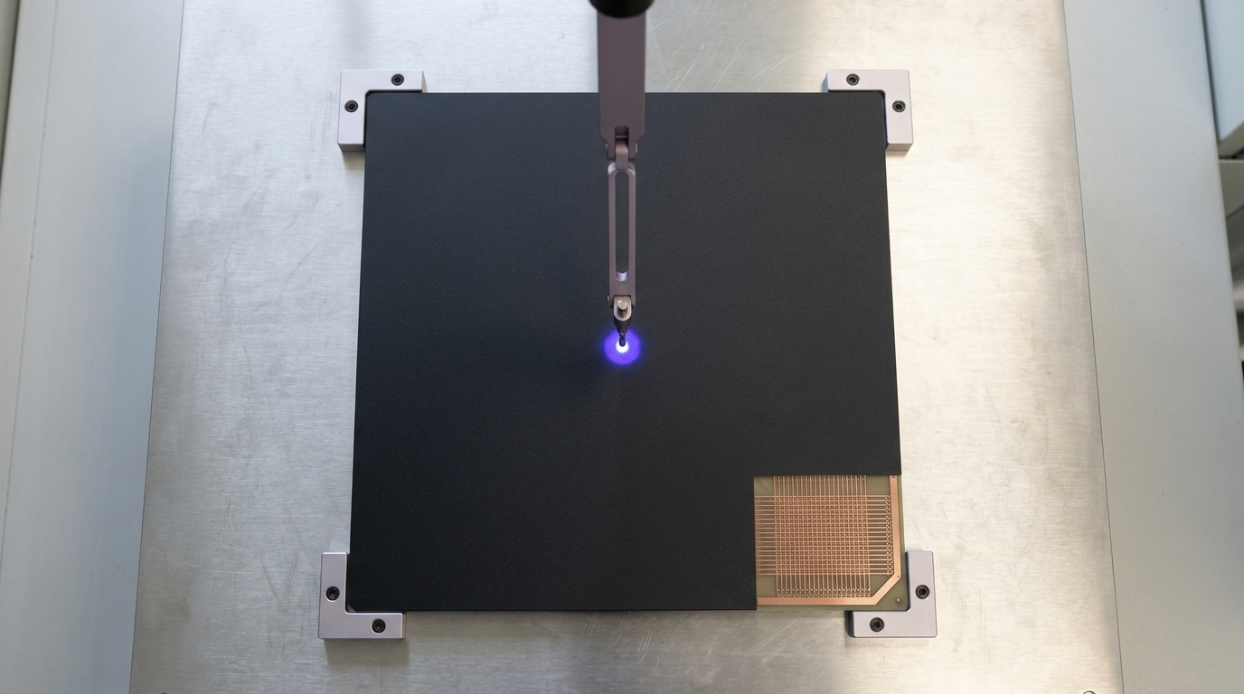
The appeal is straightforward: no separate silicon interposer means no separate silicon cost, and the RDL can be built directly at whatever panel size the molding process supports rather than being capped by a lithographic reticle field. Semiconductor Engineering’s reporting on the category is blunt about the motivation, describing large-area fan-out explicitly as “a cost-effective alternative to silicon interposers” for applications that would otherwise need one [10]. The tradeoff shows up in mechanical behaviour rather than in routing density. A molded panel made of a die embedded in epoxy compound, cured and then ground flat, is a composite of materials with different coefficients of thermal expansion, and that mismatch drives warpage during the thermal cycles of assembly and use — the semiconductor-engineering reporting on the category names “die shift” during molding and the resulting warpage as a direct yield concern specific to fan-out, distinct from anything a monolithic silicon interposer has to manage [10].
It would be easy to assume that trade cuts only one way — that fan-out buys a cost saving by accepting worse mechanical behaviour than 2.5D. A direct finite-element comparison from ASE, one of the largest outsourced assembly and test houses building both technologies, complicates that assumption rather than confirming it. Comparing 2.5D against its own FOCoS (fan-out chip-on-substrate) offering in both chip-first and chip-last process flows, ASE found that “the warpage of the two FOCoS package types are lower than 2.5D IC due to smaller CTE mismatch between combo die and stack-up substrate,” and separately that all three configurations — 2.5D, chip-first FOCoS, and chip-last FOCoS — “have similar thermal performance and all of them are good enough for high power applications” [9]. Read plainly, that is a single OSAT’s own simulation result, not an industry consensus, and it does not settle cost or bandwidth density questions at all — but it is a direct warning against assuming fan-out is the compromised option on every axis just because it is the cheaper one on this one.
3D stacking: the shortest possible path, and the heat that follows it
3D stacking abandons the lateral arrangement entirely and places one die directly on top of another, connecting the two vertically through a field of microbumps at the die faces and through-silicon vias carrying signals through the die bulk. The routing that would otherwise run sideways across an interposer or an RDL panel instead runs straight down, which is what makes 3D stacking the shortest available path between two pieces of active silicon — and, not coincidentally, why the reported pitches are already tighter than anything achievable laterally. imec’s account of current industrial practice puts 2.5D microbump pitch at “between 50µm and 30µm,” with active research pushing “to decrease the pitch to 10µm and even 5µm” for the finer end of 3D microbump stacking [6].
Shortening the electrical path this way has a direct, quantifiable effect on how much bandwidth a given joint area can carry. Treating the joint as a grid of independent connections at pitch
where
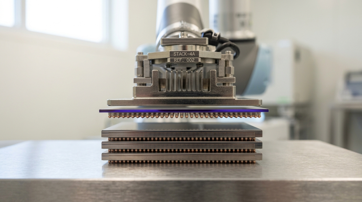
The bill for that proximity arrives as heat, and it arrives in a specific, structural way rather than as a vague “3D runs hotter” intuition. A stack has exactly one face in contact with the package’s heat-removal path — typically the topmost die, under a lid or heat spreader — so the temperature rise at a given tier depends on everything the heat has to cross to reach that face:
where
That last clause matters, because the field’s own peer-reviewed evidence does not support a blanket claim that 3D stacking is simply worse thermally than 2D or 2.5D. A study of 3D-IC architectures purpose-built for deep-neural-network accelerator dataflows found that, for the workload-matched designs they evaluated, “the 3D-IC draws similar power as 2D-ICs and is not thermal limited,” while delivering “up to 9.14x speedup” over an equivalent 2D layout on the workloads studied [11]. That is one paper’s result on one class of workload with careful co-design, not a general finding that 3D stacking is thermally free — but it is direct, citable evidence that the thermal cost of stacking is a function of how well power and placement are co-designed for the stack, not an unavoidable tax that scales with tier count alone.
Hybrid bonding: the joint that has no bump left to fail
Hybrid bonding takes the vertical topology of 3D stacking and removes the bump, the solder, and the reflow step entirely. Two wafers, or a die and a wafer, are prepared with a flat field of copper pads set into a dielectric, polished to extreme flatness by chemical mechanical polishing, brought together at room temperature, and then annealed so the copper grains grow across the interface and fuse. What is left is not two die faces joined by an intermediate material — it is, electrically and mechanically, closer to continuous copper.
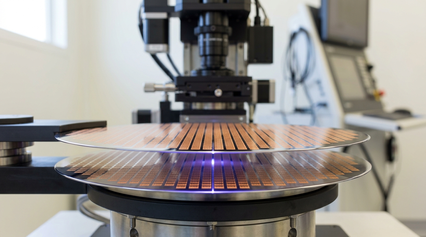
Removing the bump removes the pitch floor that bump geometry imposes, and the achieved pitches reflect it. imec reports demonstrating wafer-to-wafer hybrid bonding at “an unprecedented 400nm pitch” using a copper-and-SiCN dielectric process on full 300-millimetre wafers, describing current commercial hybrid-bonding applications as already reaching roughly one million interconnects per square millimetre at a one-micrometre pitch, with the 400-nanometre demonstration representing the technology’s next step down [7]. Reporting from Semiconductor Engineering frames the resulting advantage in terms a systems designer would recognise directly, citing AMD’s own account of the technology used in its 3D V-Cache products as delivering “15 times more interconnect density and 3 times the energy efficiency” relative to microbump-based stacking [8] — a vendor’s claim about its own product, worth reading as exactly that, but consistent in direction with the pitch numbers reported independently by imec.
That density and efficiency are bought with a categorically different kind of yield exposure than any of the other three approaches carry. A microbump joint, or a fan-out panel’s molded interconnects, has some tolerance for a defective individual connection or a modest amount of surface unevenness, because solder reflow is itself a self-aligning, gap-filling process. Hybrid bonding has essentially none. imec’s own account of the 400-nanometre pitch work states plainly that “overlay control needs to be smaller than 100nm to have sufficient yield in high-volume manufacturing” at that pitch [7], and Semiconductor Engineering’s reporting on the broader shift to hybrid bonding describes the requirement in blunter terms still, noting that the process demands “almost zero defects” and depends on tightly controlled “wafer surface cleanliness, wafer warpage, and step height between the copper and dielectric” [8]. A single sub-micrometre particle, or a few tens of nanometres of unplanned topography, is not a marginal defect in this process the way a slightly underfilled microbump might be — it can prevent the bond from forming at all across the area it touches. Cost follows the same logic: the same reporting is explicit that hybrid bonding “demands expensive equipment” and fab infrastructure that most assembly houses do not yet have, in direct contrast to the comparatively broad availability of bump-attach and reflow tooling [8].
Reading the tradeoffs on their own terms
Laid out together, the four approaches do not resolve into a ranking, because each is reported against a different unit and answers a different constraint:
| Approach | What sets bandwidth density | What sets cost | What sets thermal risk | What sets yield risk |
|---|---|---|---|---|
| 2.5D interposer | Interposer routing pitch, submicron-capable [6] | A full extra piece of processed, TSV-etched silicon [3] | Lateral layout keeps most dies close to the heat-removal face | Interposer/TSV defects; stitching yield at multi-reticle sizes |
| Fan-out (RDL panel) | RDL line/space, now approaching 2µm and below [5, 10] | No separate interposer silicon — the panel is the routing layer [10] | Comparable to 2.5D in direct simulation [9] | Die shift and warpage during molding [10] |
| 3D stacking (microbump) | Vertical pitch, tighter than any lateral geometry [6] | Added TSV and bump-attach process steps per tier | Depends on tier count and power co-design, not tier count alone [11] | Compounds across tiers; each die must be known-good before stacking |
| Hybrid bonding | Sub-micron pitch, highest reported density of the four [7] | Specialised CMP and bonding equipment most fabs lack [8] | Shortest possible path; no bump or solder layer in between | Near-zero defect tolerance; overlay control below 100nm at fine pitch [7] |
Two things are worth stating plainly about that table, because a table always tempts a reader toward a score. First, it is not one — the columns are not commensurable, and adding them would produce a number with no physical meaning. A design that needs the largest possible interposer to fit four HBM stacks next to a reticle-sized logic die is not choosing among the four rows on price; it is choosing the one row capable of the job at all, then managing that row’s specific cost and yield exposure. Second, the rows are not mutually exclusive in a finished product. It is entirely normal for a single package to combine an interposer or fan-out substrate for lateral routing with a hybrid-bonded or microbump-stacked memory tower sitting on top of it — the choice of lateral joining method and the choice of vertical joining method are made independently, exactly as the topology-versus-joining-method distinction earlier in this piece implies.
Where the field genuinely disagrees
Two live disagreements are worth naming directly, because characterising them honestly is more useful than pretending the industry has settled on an answer.
The first is whether fan-out will substitute for interposer-based 2.5D in high-performance computing generally, or remain confined to its historical mobile and networking strongholds while HPC stays on silicon interposers. The case for substitution rests on cost and on ASE’s own finding that FOCoS can match or beat 2.5D on warpage and thermal performance in direct simulation [9], combined with Semiconductor Engineering’s framing of large-area fan-out as an explicit cost-effective alternative to interposers [10]. The case against rests on what TSMC is actually building: continued investment in ever-larger multi-reticle CoWoS interposers, including the RDL-plus-silicon-bridge CoWoS-L approach specifically built to keep the largest HBM-attached accelerators on an interposer-based platform rather than moving them to fan-out [3]. Both positions are consistent with the published evidence; they are simply answers to different questions — whether fan-out is capable of replacing an interposer for a given design, versus whether the segment building the very largest AI accelerators has in fact chosen to.
The second disagreement concerns hybrid bonding’s ultimate reach: will it broaden to become the default 3D joining method across most cost tiers as equipment costs fall, or will its defect-intolerance and equipment requirements keep it confined to a premium segment indefinitely, with microbump stacking remaining the mainstream choice underneath it? Semiconductor Engineering’s own reporting on the bumps-versus-hybrid-bonding question is notable for describing this less as an active argument between camps than as a roadmap already agreed on by at least one major vendor — noting that Intel’s own published plans extend microbump use for a period while migrating later to hybrid bonding, which the reporting characterises as complementary roles on a timeline rather than a live contest for the same designs today [8]. Where that leaves genuine uncertainty is how fast the migration proceeds and how far down the cost tiers hybrid bonding eventually reaches — a question the currently available reporting does not resolve, and this article does not attempt to resolve it either.
Forecasts, with what would disconfirm each
These are predictions, kept explicitly separate from the sourced comparison above. Horizon: 15 August 2029. Common assumptions: no discontinuity in EUV lithography roadmaps; continued demand growth for large accelerator packages; no supply disruption removing a major OSAT region from the market.
One. 2.5D silicon interposers and fan-out RDL panels will continue to coexist as distinct product lines rather than one displacing the other, because they are chosen for different reasons — reticle-busting interposer area versus cost and panel-size flexibility. Indicators: continued parallel roadmap investment by the same OSATs and foundries in both interposer and large-area fan-out lines. Disconfirmed if a major foundry or OSAT publicly discontinues one product line in favour of the other for HPC-class parts.
Two. Microbump 3D stacking will remain the majority joining method for 3D packages by shipped volume through the horizon, even as hybrid bonding’s share grows, because equipment cost and defect tolerance favour bumps outside the highest-value segments. Indicators: continued high-volume bump-attach tool orders alongside hybrid-bonding equipment orders. Disconfirmed if published unit-volume data shows hybrid bonding exceeding microbump stacking in shipped 3D packages before the horizon.
Three. Reported hybrid-bonding pitch will continue to improve faster than reported bandwidth-per-watt for microbump stacking, because pitch is the cheaper lever in the bandwidth-density relationship derived above, and hybrid bonding has more pitch headroom left to give. Indicators: successive published hybrid-bonding pitch records outpacing published microbump pitch or power-efficiency records over the same interval. Disconfirmed if a mainstream microbump specification closes more than half the current pitch gap with hybrid bonding.
Four. Thermal co-design — power-tier placement and workload-aware stacking — rather than a hardware fix such as microfluidic cooling, will account for most of the improvement in what stack heights are considered viable. Indicators: published 3D-IC design methodologies increasingly citing power-tier placement rather than novel cooling hardware as the primary lever. Disconfirmed if the leading published viability gains through the horizon are attributed chiefly to new cooling hardware rather than to placement and co-design.
None of these requires a technological surprise. They follow from the physical relationships already on the table: bandwidth density that scales with the inverse square of pitch, a thermal path defined by how many layers sit between a tier and the heat sink, and a yield exposure that differs in kind, not just degree, between a process with reflow to fall back on and one without.
What to take away
There is no single best way to join two pieces of silicon, and the four approaches compared here are not competing to become one. A 2.5D interposer buys submicron lateral routing at the price of a second piece of processed silicon. Fan-out buys a comparable lateral routing job without that silicon, at the price of a warpage and die-shift risk specific to a molded, mixed-material panel. 3D stacking buys the shortest possible electrical path by going vertical, at the price of a thermal design problem that depends on tier placement rather than tier count alone. Hybrid bonding buys the tightest pitch and highest density of any of the four by removing the bump entirely, at the price of a near-zero defect tolerance that the other three approaches simply do not have to meet.
The practical discipline that follows is to stop asking which packaging technology is “best” and start asking which specific constraint a given design is actually up against — reticle-exceeding routing area, panel-level cost, vertical bandwidth, or absolute interconnect density — because that constraint, not a general reputation, is what the published comparisons above actually measure.