The unit of design moved off the die
For three decades the interesting question in semiconductors was what happened inside one piece of silicon, and the packaging around it was a solved problem that mostly determined how the part was soldered down. That relationship has inverted. On the systems that matter most commercially in 2026 — large accelerators for machine learning, and the memory attached to them — the die is no longer the unit of design. The package is. The substrate, the interposer, the bonding pitch and the assembly line are where the remaining performance is being found, and increasingly where the supply is being lost.
This is not a rhetorical flourish about Moore’s law. It is a statement about where the binding constraints sit, and each one can be named. A single die cannot exceed the area a lithography scanner can expose in one shot. Below that ceiling, cost per good die grows faster than area because defects accumulate. Above a certain system size, the only way forward is to build the system from several pieces — and the moment you do, a wire that used to be a short on-die trace becomes a link that has to leave one piece of silicon and enter another. That transition is expensive in a very specific and measurable way, and the whole discipline of advanced packaging is the effort to make it less so.
The through-line of everything below is one quantity: the energy required to move a bit, as a function of the distance it travels. Nearly every technique in advanced packaging — finer bumps, interposers, vertical stacking, memory placed beside logic — is an attempt to shorten that distance or widen the path, and nearly every cost, thermal and yield problem in the field is the price of doing so.
Two ceilings on one large die
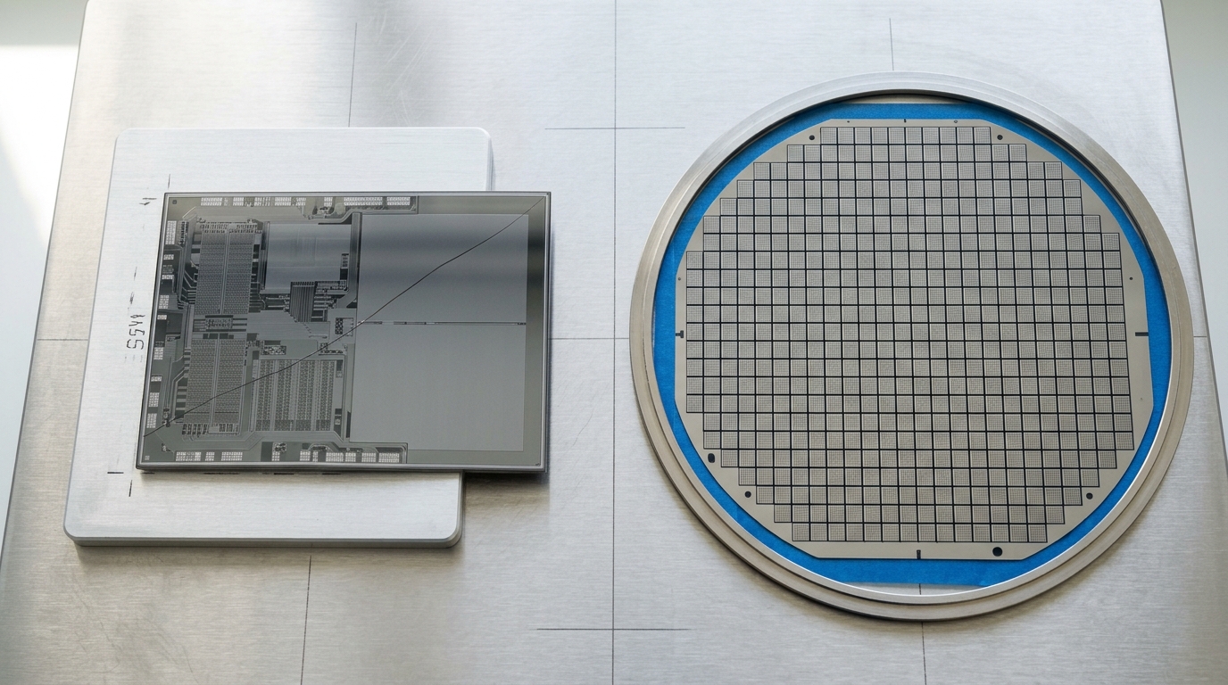
The first ceiling is optical and hard. A lithography scanner exposes a rectangular field, and a die cannot be larger than what one exposure can print without stitching two exposures together. Standard extreme-ultraviolet systems use a field of 26 by 33 millimetres. The move to high numerical aperture, described by ASML’s Jan van Schoot, raises the numerical aperture from 0.33 to a target of 0.55, and pays for it by doubling the demagnification in the single direction where the largest reflective angles occur — which reduces the printable field to roughly half its former size, about 26 by 16.5 millimetres [1]. The most advanced lithography available therefore prints smaller maximum dies than the generation before it. Anyone wanting a physically large system on the newest process must either stitch fields together or stop trying to build one die.
The second ceiling is statistical and softer, but it bites earlier. Defects arrive on a wafer at some density, and the probability that a given die contains none of them falls as its area grows. Feng and Ma, in the cost model they published for multi-chiplet architectures, use the negative binomial form
with defect density
Their quantitative conclusion is more careful than the popular version of it. At advanced nodes with large dies, they find multi-chip integration can save up to half the die cost; at a mature 14-nanometre node the yield-driven saving is up to about a third but the overall cost advantage is, in their words, “not that significant” [2]. And crucially: “for a single system, monolithic SoC is often a better choice unless the area or the production quantity is large enough.” Disaggregation is not a universal improvement. It is a trade that wins at large area, advanced nodes and high volume, and loses elsewhere.
Cutting creates a boundary you then have to pay for
Suppose the trade is worth it. You cut the design into chiplets. What you have actually done is take a set of wires that ran inside one piece of silicon and promote them into an inter-die interface with its own transmitters, receivers, clocking, training, error handling and physical connectors. The interface is now the design boundary in every sense: architectural, electrical, organisational and commercial. Partitioning is chosen not by what is conceptually tidy but by where the required bandwidth across a cut is low enough to afford.

This reframes a familiar architectural question. On a monolithic die, “where should this block go” is a floorplanning problem with soft costs. Across a chiplet boundary it is a bandwidth budget with hard costs in area, power and package complexity. Caches, coherence traffic and memory controllers are the usual casualties: they are exactly the structures that assume cheap, wide, low-latency access to everything. Designers respond by keeping the highest-traffic relationships inside a die and pushing lower-traffic relationships across the boundary — which is the same logic as deciding which parts of a marquetry pattern can be cut as separate pieces without putting a joint through the place that carries the load.
Energy per bit is a function of distance
Here is the physical core. To first order, a short parallel die-to-die link is a driven capacitive wire, and the energy spent per bit is set by the capacitance that must be charged and discharged:
where
Within its range of validity, the model explains the entire strategy of advanced packaging. Shorten
The public specifications put figures on it. The Open Compute Project’s Bunch of Wires physical-layer specification, an open die-to-die standard deliberately designed to run over both ordinary organic laminate and advanced packaging, states targets of under 0.5 to 1 picojoule per bit for doubly terminated modes and under 0.25 to 0.5 picojoule per bit for unterminated ones, at throughput densities of up to 2 to 12 or more terabits per second per millimetre of chip edge, and portability across process nodes from 65 nanometres to 5 nanometres [5]. The point is not the precise value; it is the ratio between these numbers and what it costs to drive the same bit across a printed circuit board, and the fact that the specification explicitly trades throughput per chip edge against design complexity, cost and packaging technology. That trade is the whole discipline in one sentence.
What proximity buys in 2.5D
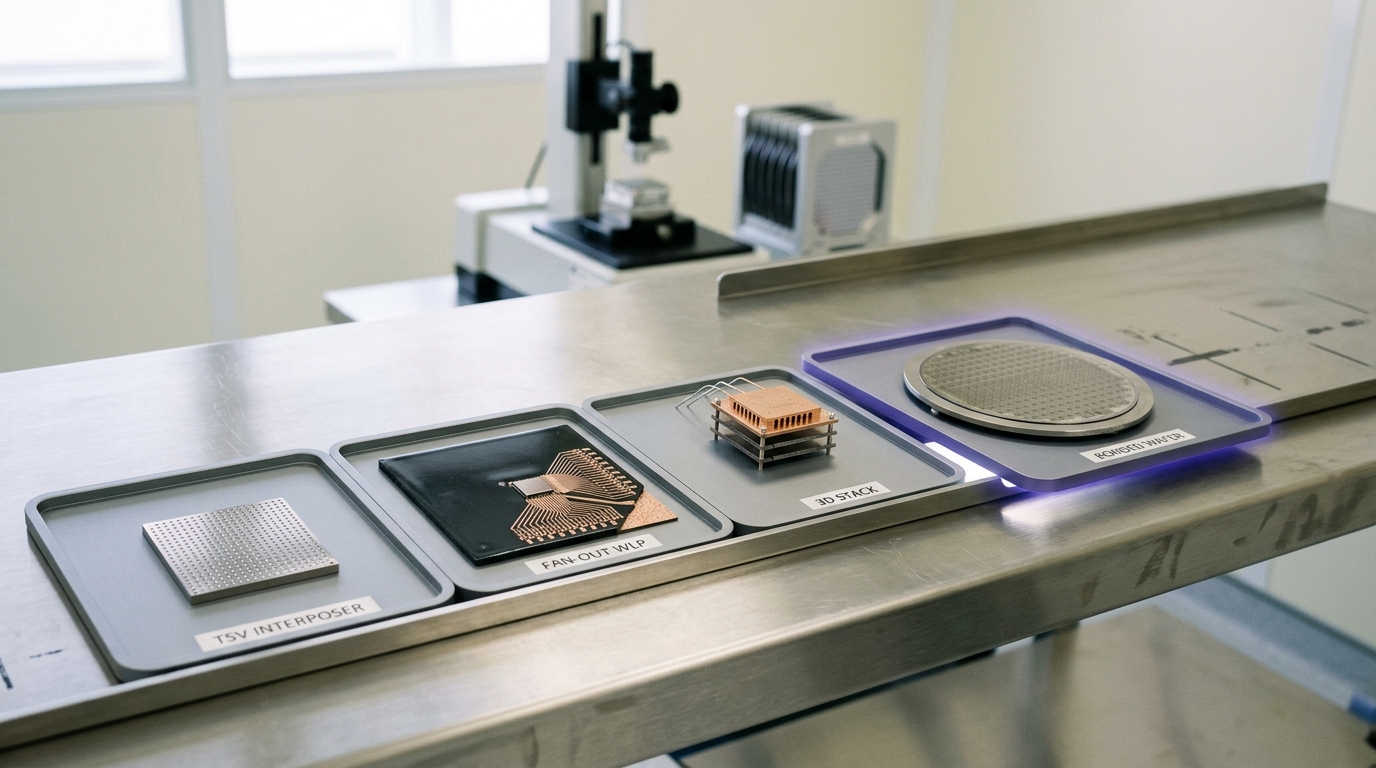
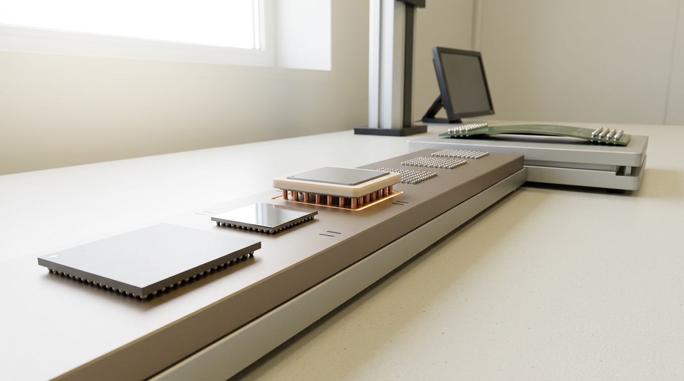
A 2.5D package sets several dies side by side on a shared high-density carrier — a silicon interposer or a fine redistribution layer — so that connections between them run through a medium with far finer geometry than a circuit board. The relevant parameter is pitch, because pitch sets how many conductors cross a millimetre of die edge.
The trajectory is well documented. Beyne and Van der Plas at imec describe microbump pitches in industrial use between 50 and 30 micrometres, with imec targeting 10 and even 5 micrometres, and redistribution-layer pitches targeted at 2 micrometres with submicron work further out [6]. Halving a pitch roughly doubles the number of wires per millimetre of edge and quadruples the connections available per unit area. That is a bandwidth multiplier obtained without raising the per-wire rate at all — the cheapest kind of bandwidth there is, since it does not cost signalling energy.
The vendor claims sit on top of this substrate story and should be read as claims. NVIDIA states that its Blackwell products consist of two reticle-limited dies joined by a 10-terabyte-per-second chip-to-chip interconnect operating as a single unified GPU, with 208 billion transistors on a custom TSMC 4NP process [7]. That is a company describing its own product; the figure is a specification, not an independently reproduced measurement. What is architecturally informative in it is the phrase “reticle-limited”: the design is explicitly organised around the optical ceiling described earlier, and the interconnect exists to make the resulting seam invisible to software.
Stacking upward, and the heat that follows
3D integration goes further and puts silicon on silicon, connecting vertically through the wafer with through-silicon vias, or bonding dies face to face without solder at all. The pitch improvement is dramatic. Wafer-to-wafer hybrid bonding reaches interconnect pitches down to 400 nanometres with roadmap forecasts of 200 nanometres, while die-to-wafer bonding operates at a few micrometres [6]. The UCIe consortium’s own specification summary reflects the same shift, describing 3D bump pitches ranging from around 10 to 25 micrometres down to one micrometre or less [3]. At those pitches the vertical connection is no longer meaningfully a “link” — the distance term in the energy expression nearly vanishes and what remains is close to an on-die wire.
The bill arrives as heat. Emma and Kurshan, surveying 3D system design, name higher power density as the direct consequence of improved packaging density, alongside the requirement that layers be co-designed for spatial correspondence and that each layer be independently testable before assembly [9]. The geometry is unforgiving: a stack has one face against the heat sink, so every additional tier sits behind the thermal resistance of everything below it. Barua, Udoy and Aziz, reviewing thermal modelling for heterogeneous 3D integrated circuits, emphasise that as power densities rise and dies stack, heat removal paths become constricted and junction temperatures rise, with thermal boundary resistance and variability in thermal interface materials playing a central role — and they warn specifically against decoupled electrical and thermal analysis, since the two are coupled through leakage and timing [10].

The practical consequence is that stacking is not applied uniformly. It is applied where the vertical bandwidth gain is largest and the power density added is smallest, which is why the earliest and most durable commercial uses of vertical stacking have been memory on memory, and memory or cache placed against logic, rather than hot logic placed on hot logic.
Memory beside logic, because the alternative is worse
Stacked memory adjacent to logic is not a fashion. It is the direct structural response to the bandwidth constraint that the energy model predicts. If moving a bit costs energy proportional to distance, then the working set of a large model — which must be streamed repeatedly — should be placed as close to the arithmetic as physics and manufacturing allow. High-bandwidth memory does exactly that: it stacks DRAM dies vertically, connects them through the stack, and places the stack on the same package carrier as the processor, replacing a long board-level bus with a very wide, very short on-package one.
The generational figures come from the memory vendors and should be attributed to them. SK hynix announced in September 2025 that it had completed development of HBM4 and prepared it for mass production, claiming 2,048 input/output terminals — double the previous generation — an operating speed of over 10 gigabits per second per pin against a JEDEC standard speed of 8 gigabits per second, more than 40 percent improved power efficiency, an advanced mass-reflow molded underfill assembly process, and a projected improvement of up to 69 percent in AI service performance where deployed [8]. Every one of those is a manufacturer claim about its own product. The structural fact underneath them is not in dispute and is more interesting than the numbers: the industry chose to widen the interface rather than only speed it up. Doubling the wires at a modest per-pin rate is the packaging-side answer, and it is available only because the memory sits on the same carrier as the logic. It is the same trade as the die-to-die interfaces above, made at a larger scale.
Yield compounds, and testing becomes the economics
A multi-die package inherits a property that a single die does not have: its yield is a product, not a term. If a package contains dies with individual probabilities
Multiplication is brutal at scale. Eight components at 99 percent each land near 92 percent together before assembly loss is counted; the same eight at 95 percent land near 66 percent. And the loss is not proportional to the failing part — scrapping a package destroys every good die in it plus the assembly work. This is precisely why known-good-die testing dominates the discussion: the whole point is to move the
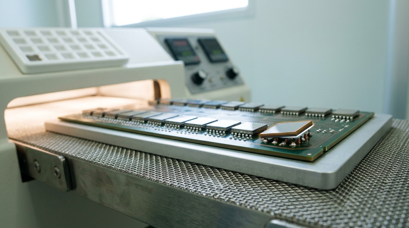
Feng and Ma model this explicitly, treating the cost of wasted known-good dies caused by packaging defects as its own term, and reaching a conclusion that reads as the field’s summary judgement: “multi-chip architecture begins to pay off when the cost of die defects exceeds the total cost resulting from packaging” [2]. Chiplets are not free bandwidth; they are a bet that the yield you recover on small dies exceeds the yield and cost you surrender at assembly. Emma and Kurshan make the same point from the design side, listing independent testability of each layer prior to assembly and yield management during assembly and final test among the defining challenges of 3D systems [9]. The IEEE Electronics Packaging Society’s Heterogeneous Integration Roadmap, produced with SEMI and other societies as a fifteen-year forecast of industry requirements, carries a dedicated Test working group alongside its groups on interconnects for 2D and 3D architectures and on multi-chip integration — an organisational signal that test is treated as a first-class discipline in this domain rather than a downstream step [11].
Substrate and assembly are a separate supply constraint
There is a persistent tendency to treat “chip supply” as one thing measured in wafers. Advanced packaging breaks that assumption. Interposers, high-layer-count organic substrates, bonders, molding and test are different equipment in different buildings, often owned by different companies, and their capacity does not move when wafer capacity moves.
Reporting through 2026 has been consistent about where the tightness sits. TrendForce, citing Taiwanese financial press and institutional investors, reported in June 2026 that the CoWoS supply-demand gap was expected to narrow from roughly 20 percent to roughly 10 percent by the end of 2026, with TSMC’s monthly capacity put at 120,000 to 140,000 wafers and outsourced assembly and test partners contributing a further 50,000 to 60,000, approaching 200,000 wafers per month in total; the same report cited TSMC, via Reuters, forecasting a compound annual growth rate above 80 percent for its advanced packaging capacity from 2022 to 2027, and placed panel-level packaging qualification and pilot production in 2026 and 2027 respectively [12]. These are third-party estimates of a private company’s capacity and should be treated as such — the direction is well corroborated, the specific numbers are not audited.
The structural analysis of that exposure is longer-standing. Noor and colleagues, surveying the microelectronics packaging ecosystem, describe the industry’s shift from device miniaturisation toward heterogeneous integration and identify bottlenecks and weak links in the advanced packaging supply chain, together with the concentration of outsourced assembly and test capability offshore and the resulting policy interest in building domestic capability [13]. The important inference for anyone reasoning about capacity is simply this: a foundry can add wafer starts and still not be able to ship more finished accelerators, because the constraint has moved downstream of the wafer.
Standardising the boundary, and what is still unsettled
If the die-to-die interface is the new design boundary, then whether it is proprietary or standard determines whether chiplets remain an internal manufacturing technique or become a market. Two efforts define the current landscape. The UCIe consortium’s specification family has progressed from a die-to-die interconnect with a physical layer, protocol stack, software model and compliance programme, through a revision adding 3D packaging support at bump pitches from around 10 to 25 micrometres down to one micrometre or less, to a version supporting 48 and 64 gigatransfers per second — double the previous 32 — with an extended sideband channel reaching up to 100 millimetres [3]. The consortium describes the 3.0 revision as doubling throughput for both two-dimensional and 2.5D chiplet designs while adding runtime transmitter-side recalibration and an optimised idle state for power gating, and states that backward compatibility is maintained [4]. Alongside it, the Open Compute Project’s Bunch of Wires physical layer targets the same job from a different angle, deliberately spanning commodity laminate as well as advanced packaging and giving adopters explicit freedom to trade throughput per chip edge against complexity and cost [5].
Experts do not agree on what this adds up to, and the disagreement is worth characterising rather than resolving. One position holds that a standard electrical and protocol interface is the necessary and nearly sufficient condition for an open chiplet marketplace, and that the remaining work is compliance and business practice. A second holds that the electrical interface was never the hard part — that thermal co-design, mechanical stress, test escape attribution, warranty allocation when a package fails, and the sheer co-design implied by shared interposer floorplans keep multi-vendor assembly economically internal for the foreseeable future. A third position, visible in the specifications themselves, is that the useful outcome is not a marketplace at all but reuse: the same interface letting one vendor mix its own dies across nodes and generations. The published record supports the observation that both standards explicitly parameterise the packaging trade-off rather than mandating a single package type — which is what you would design if you expected the answer to differ by product, and is at least mildly evidence against the strong marketplace thesis.
Forecasts, with the observation that would refute each
These are predictions, separated from the sourced analysis above. Horizon: 8 August 2029. Common assumptions: no discontinuity in lithography beyond the announced high-numerical-aperture path; continued growth in demand for large accelerator systems; no geopolitical event that removes a major assembly region from supply.
One. Packaging and assembly, not wafer fabrication, will remain the binding constraint on large-accelerator shipments through the horizon. Indicators: continued reporting of a supply-demand gap in advanced packaging capacity, and capital expenditure guidance weighted toward assembly and substrate. Disconfirmed if leading suppliers report advanced packaging utilisation materially below wafer utilisation for four consecutive quarters.
Two. The maximum die area used in new high-performance designs will not rise, and multi-die construction will become the default rather than the exception at the leading node. Indicators: new flagship parts described in terms of tile or chiplet count rather than die size. Disconfirmed if a leading-node flagship ships as a single stitched die larger than a full standard reticle field.
Three. Reported energy per bit for standard die-to-die interfaces will improve more slowly than aggregate package bandwidth, because bandwidth will be bought mainly with pitch and width rather than with signalling efficiency. Indicators: successive specification revisions emphasising bump pitch and wire count over per-wire power. Disconfirmed if a mainstream published interface halves its per-bit energy at constant pitch.
Four. Known-good-die test coverage and its cost will be discussed publicly as a first-order design parameter, not a manufacturing detail. Indicators: test strategy appearing in architecture disclosures and standards work. Disconfirmed if the major die-to-die standards ship through the horizon with no expanded test and repair provisions.
None of these requires a breakthrough. They follow from the arithmetic already on the table: a fixed optical field, a yield that falls with area, a yield that multiplies across a package, and an energy per bit that rises with distance.
What to take away
Advanced packaging is not a supporting technology that happens to be scarce. It is where the design now happens. The reticle field sets a hard ceiling on one piece of silicon; the yield curve makes approaching that ceiling expensive well before you reach it; so systems are cut into pieces, and the cut creates an interface whose cost is governed by how far a bit must travel and how many conductors can be crossed per millimetre of edge. Every subsequent technique — finer bumps, interposers, through-silicon vias, hybrid bonding, memory stacked beside logic — is a way of shortening that distance or widening that path, and every one of them is paid for in heat, in compounded yield, and in a category of factory capacity that is not measured in wafers.
The practical discipline that follows is to stop reading a system’s specification as a property of its silicon. Ask how many pieces it is made of, what crosses each boundary and at what energy, which face of the stack touches the heat sink, what the assembly yield is, and who has the substrate. Those questions now explain more of the observed performance and more of the observed availability than the process node on the label does.