Before the word “chiplet”
Every history of advanced packaging risks being written backward: start from the accelerator packages of the mid-2020s, work back to whatever looks like a precedent, and the past becomes a tidy staircase leading to the present. The dated record does not cooperate with that shape. The industry built a dense multi-die package in 1980, walked away from the approach for most of two decades because the economics did not work, rebuilt the physical toolkit for different reasons in the 2000s, and only then, forced by its own proprietary fragmentation, sat down in 2022 to agree on a shared way of doing what it had already relearned how to do twice.
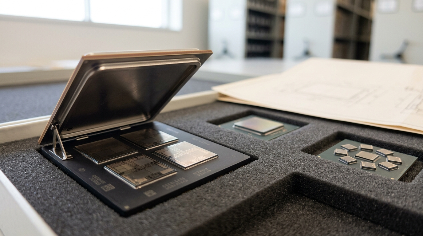
This article follows that sequence in order, with a date and a citable source attached to each claim. It is a history of objects and decisions, not of ideas in the abstract: a ceramic block with a hundred chips glued to it, a tray of untested die that ruined a manufacturing line’s yield, a slab of silicon with vertical holes drilled through it, a processor with its heat-spreader lifted to show four separate pieces of silicon underneath, and a specification ten companies signed at once. Vendor claims are marked as vendor claims throughout; where a figure comes from a company’s own announcement about its own product, the text says so.

1980: a hundred chips on one block of ceramic
The starting point most historical accounts of advanced packaging skip is also the most literal one. In 1980, IBM introduced the Thermal Conduction Module for its 3081 mainframe processor: a multichip module carrying on the order of a hundred high-speed integrated circuits on a single ceramic substrate built up from roughly three dozen internal wiring layers [1]. The engineering problem the TCM solved was not density alone but density paired with heat. Each chip sat under its own small metal piston, the pistons surrounded by helium because helium conducts heat far better than air, and the entire module was water-cooled from outside [1]. A single board built around these modules in IBM’s later 3090 system drew on the order of 1,400 amps, a figure that says more about the era’s tolerance for extreme engineering in pursuit of density than about any specific design elegance [1]. The same packaging concept carried across three generations of IBM mainframes: the 3081 in 1980, the 3090 in 1985, and the System/390 in 1990 [1].
None of this used the word “chiplet,” and none of it was built for the reason chiplets are built today. IBM’s motivation was interconnect density and signal delay between chips that a single die of the era’s process technology could not internally accommodate, not a yield or reticle-size problem in the sense the industry means those terms now. But the structural bet — accept the cost and complexity of joining several separately manufactured pieces of silicon on one substrate, in exchange for a level of density and performance no single chip of the era could reach alone — is the same bet every later chapter of this history revisits. A retrospective account of packaging’s evolution published in 2026 makes the same connection explicitly, citing the era’s thermal conduction modules alongside IBM’s 1991-era 9121 multichip module as early instances of exactly the heterogeneous, disaggregated design pattern that a modern industry treats as new [14].

The 1990s: a technology that “never materialized”
If the 1980s established that multichip packaging could work, the 1990s established, in painful commercial detail, why it usually did not pay. Multichip module research was genuinely active across the decade — ceramic, laminate and deposited thin-film variants were all pursued in parallel — but the high-volume manufacturing the research anticipated did not follow. John Lau, a long-time figure in 3D IC and packaging research writing a retrospective in 2017, put it bluntly: “There was much research performed on MCMs during the 1990s. Unfortunately, at that time, due to the high-cost of ceramic and silicon substrates and the limitation of line width and spacing of the laminate substrate, the high volume manufacturing (HVM) of MCMs never materialized” [2]. His account of the aftermath is even more direct: for a long stretch afterward, he writes, “MCM has been a ‘dirty’ word in semiconductor packaging” [2].
The arithmetic behind that reputation is straightforward and still governs every multi-die package built today. A packaged part’s yield is not the yield of its worst component; it is the product of every component’s yield together with the yield of the assembly step that joins them. Write the package yield
Multiplication is unforgiving at scale. Every die added to a package is another factor less than one, so a package holding several die each individually manufactured at a very respectable yield can still fail at an uncomfortable rate overall, and every one of those failures scraps every good die sealed alongside the bad one. A 2023 survey of the US packaging ecosystem frames the resulting industry response in exactly these terms, identifying “enhancing yield to achieve cost reduction” as one of the core drivers of heterogeneous integration and noting that “by integrating known good dies or chiplets with a higher manufacturing yield,” a multi-die approach can raise the effective yield of the finished system even where a single large die would not have been manufacturable at an acceptable rate at all [3]. That is the promise. The 1990s discovered that realizing it required testing every individual die to a packaged-part standard before committing it to an assembly that could not be undone — the “known good die” problem — and that this testing was itself expensive enough, on top of the era’s costly ceramic and laminate substrates, to erase much of the yield advantage multichip modules were supposed to deliver [2] [3].
A later, more formal treatment of the same trade-off, published as a cost model for chiplet architectures in 2022, states the underlying logic as a threshold rather than a universal rule: a multi-chip approach pays for itself once the cost of die defects in a monolithic design exceeds the total cost the packaging step adds [4]. In the 1990s, for most products at the process nodes and die sizes then in commercial use, that threshold was not crossed. The multichip module was not a failed idea; it was a correct idea applied a decade or two before the die sizes, defect densities and testing economics needed to clear its own break-even point.

2000s to 2012: the vertical route matures, and TSMC ships an interposer
The 2000s did not revive the multichip module directly. Instead, a separate research thread matured that would eventually give packaging a new physical toolkit: the through-silicon via, a vertical electrical connection drilled and plated through a piece of silicon rather than routed only across its surface. A 2017 peer-reviewed survey of the technology describes through-silicon vias as “a promising candidate” for extending system performance past the limits of shrinking transistors alone, and traces their eventual use across memory, imaging, MEMS and bioapplication devices — while noting candidly that, even by the time of that survey, the technology’s fabrication cost still kept it from being “generally implemented” as a default packaging choice [5]. That caveat is worth sitting with: through-silicon vias were a mature research subject for years before they were an economical manufacturing default, which is a large part of why this technology’s commercial debut lagged its academic one by roughly a decade.
The commercial debut, when it came, was TSMC’s. The company’s own technology documentation describes its Chip-on-Wafer-on-Substrate platform, CoWoS, as “a wafer level system integration platform” for stacking multiple dies on a silicon interposer, and dates its earliest customer products to 2012, built for Xilinx field-programmable gate arrays [6]. Independent trade coverage narrows that timeline further: an industry account of the Xilinx-TSMC collaboration places the technology’s formal announcement at a third-quarter-2011 investor event, with production ramping through 2012 and 2013 [7], while a contemporaneous DIGITIMES report dated 27 October 2011 states that Xilinx had begun “the first shipments of its Virtex-7 2000T FPGA, the first product using 2.5D IC stacked packaging technology” [8]. By October 2013, TSMC and Xilinx announced that all of Xilinx’s 28-nanometre 3D IC families were in volume production, including a heterogeneous Virtex-7 HT family the companies described as the industry’s first heterogeneous 3D ICs to reach production [7].
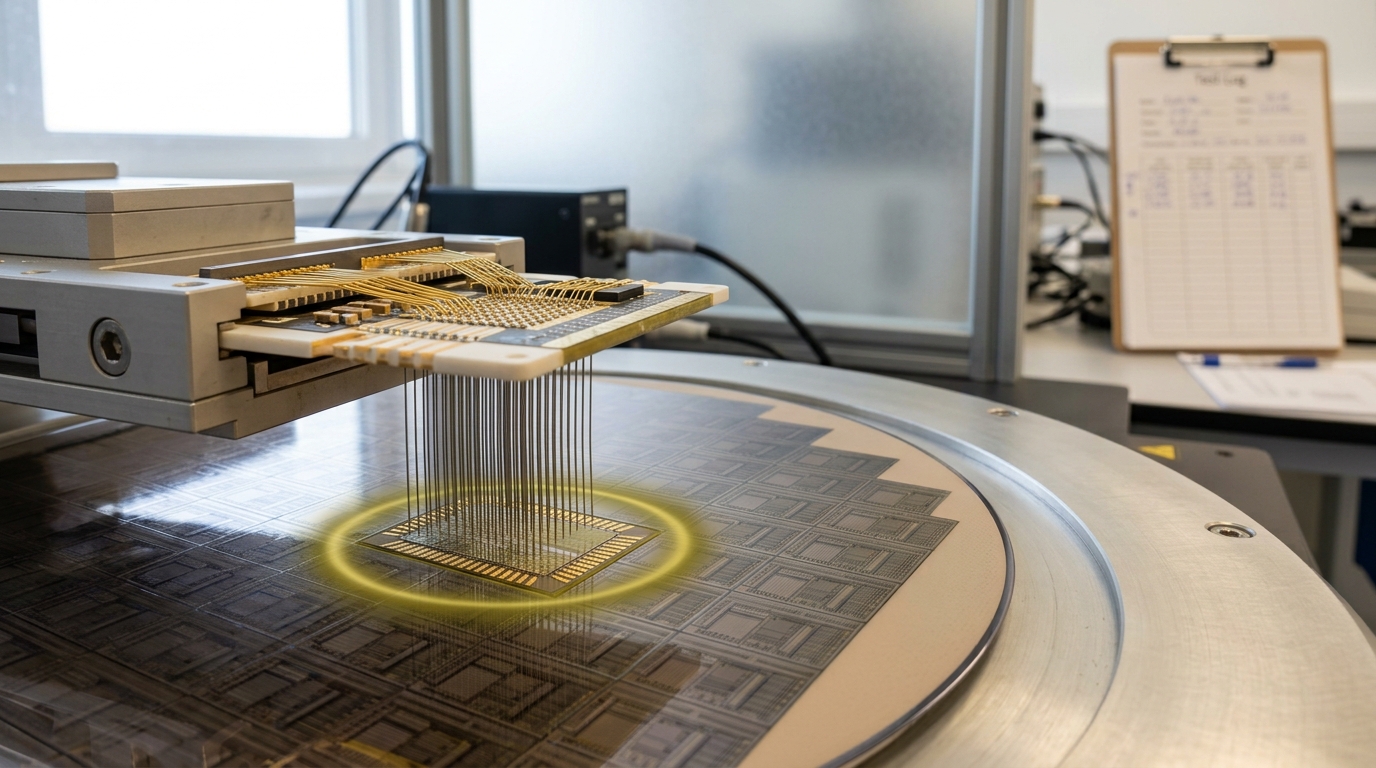
What CoWoS actually did, mechanically, is worth stating plainly because it is the direct physical ancestor of every large accelerator package built since. Multiple dies are bonded onto a passive silicon interposer — a slab of silicon that carries no active transistors of its own but is threaded with through-silicon vias and fine surface wiring — which is in turn attached to an ordinary organic package substrate [3]. The interposer’s job is purely to let the dies on top of it talk to each other, and to the substrate below, at a wiring pitch far finer than any board-level connection could offer. This is the “2.5D” label the industry still uses today: dies placed side by side rather than stacked directly on one another, but joined through an intermediate layer built with silicon-fabrication precision rather than circuit-board precision. Every part of that description — passive interposer, through-silicon vias, fine redistribution wiring beneath dies placed side by side — traces to research that matured across the 2000s and reached a shipping product only in 2012 [5] [6].
2017: AMD reaches for the multichip module again
By the mid-2010s, the reticle-limited, defect-density economics that the multichip module’s 1990s failure had run ahead of finally caught up with it, at least for one company’s server processors. AMD’s EPYC datacenter processor, launched on 20 June 2017, was described in the company’s own announcement as “a highly scalable System on Chip (SoC) design” offering up to 32 “Zen” cores across a product line running from an eight-core EPYC 7251 up to a 32-core EPYC 7601, connected across sockets by AMD’s Infinity Fabric interconnect [9]. What that press release does not spell out, and what a peer-reviewed account of the underlying silicon does, is that this was a multichip module in the direct lineage of the 1980s and 1990s design pattern: a single die design, code-named Zeppelin, built on a 14-nanometre FinFET process at roughly 4.8 billion transistors and 213 square millimetres, that could be packaged as one, two, or four identical dies depending on the target market [10]. The paper describing Zeppelin, published in the IEEE Journal of Solid-State Circuits, credits AMD’s Infinity Fabric with extending a coherent, scalable on-die data fabric across “up to eight dies across two packages,” using a purpose-built physical-layer link for the inter-die hop specifically [10]. The four-die configuration was EPYC, marketed under the code name Naples; the same die, packaged singly, became AMD’s mainstream desktop parts, and packaged in pairs became its high-end desktop line [10].
The economic logic is the same one the 1990s multichip module could not clear. A single monolithic die carrying the equivalent of four Zeppelin dies’ worth of logic would have been substantially larger, and by the yield mathematics above, substantially more expensive per good unit at any given defect density — while four smaller dies, individually tested before assembly, could be combined with a known, bounded assembly-yield penalty [4]. By 2017, unlike in the early 1990s, that trade had become favourable enough for at least one major vendor to build a flagship server product around it.
2019: AMD splits the die on purpose
Naples used four copies of one die. Two years later, AMD’s second-generation EPYC processor, code-named Rome and launched on 7 August 2019, went further: it deliberately split compute and input/output logic onto two different dies built on two different process nodes. AMD’s own launch announcement describes the 2nd Gen EPYC line as delivering up to 64 “Zen 2” cores per SoC on a 7-nanometre process, roughly double the performance of the prior generation and up to 23 percent higher instructions-per-clock on server workloads, alongside four times the L3 cache [12]. Those are the vendor’s own comparative claims about its own products and should be read as such. The architectural description independent of AMD’s marketing comes from a University of Utah high-performance-computing technical review published the same year: “The Rome design consists of 7 nm process CPU chiplets and 14 nm process I/O die, which connects to all the chiplets and creates a more uniform core hierarchy as compared to the Naples. The smaller chiplet production is easier and cheaper than larger monolithic CPU” [11]. Concretely, the review describes eight compute chiplets, each an eight-core “Core Complex Die” built on the new 7-nanometre process, arranged around one central input/output die built on the older, cheaper 14-nanometre process and connected to every compute chiplet by AMD’s second-generation Infinity Fabric [11].
This is the moment the historical record supports calling a genuine chiplet design rather than a multichip module in the 1980s or 2017 sense. Naples combined four identical dies from one design and one process; Rome combined two structurally different die types, deliberately fabricated on two different process nodes chosen for what each part of the design actually needed — the newest, most expensive process for the logic that benefited most from it, an older and cheaper process for input/output circuitry that gained comparatively little from further shrinking. That distinction — heterogeneity by design, not just multiplicity of identical parts — is what separates a chiplet architecture from a multichip module built purely for yield or area reasons, and AMD’s own two-year gap between Naples and Rome is a dated record of the industry making that exact transition inside a single product line.
The cost of doing it alone
Once more than one vendor had committed to multi-die packages built around silicon interposers or bridge-based interconnects, each vendor’s approach diverged in a way that a single company’s internal engineering teams had no strong incentive to reconcile. The 2023 survey of the US packaging ecosystem lists the resulting fragmentation by name: TSMC’s local silicon interconnect, Intel’s Embedded Multi-die Interconnect Bridge (EMIB) as an example of bridge-based 2.5D packaging where a small silicon bridge is embedded directly in the package substrate rather than using a full interposer, and ASE’s stacked silicon-bridge fan-out chip-on-substrate approach, among others, each solving the same die-to-die connectivity problem with an incompatible physical and electrical interface [3]. AMD’s own Infinity Fabric, described above, was itself a proprietary die-to-die physical layer, built to connect AMD’s own dies to each other and never intended to connect to anyone else’s [10].
The practical consequence was that a chiplet designed to sit inside one company’s package could not be reused inside a different company’s package, even where the physical packaging technology available — TSMC’s interposers, for instance — was shared across customers. Every vendor building a multi-die product was independently re-solving the physical layer, the protocol stack, and the compliance testing for its own die-to-die links, with no shared foundation to build on and no path for a specialised chiplet maker to sell into more than one company’s ecosystem. That, rather than any single technical limitation, is the problem the next date in this history was convened to solve.

2 March 2022: ten companies write one specification
On 2 March 2022, in Beaverton, Oregon, ten companies announced the formation of an industry consortium to standardize exactly the die-to-die interconnect problem the preceding years had left fragmented. The founding companies’ own press release names them: Advanced Semiconductor Engineering (ASE), AMD, Arm, Google Cloud, Intel, Meta, Microsoft, Qualcomm, Samsung, and TSMC, “announced the formation of an industry consortium that will establish a die-to-die interconnect standard and foster an open chiplet ecosystem” [13]. The same announcement states that the founding companies had already ratified a first version of the specification: “UCIe 1.0 specification ratified to provide a complete standardized die-to-die interconnect with physical layer, protocol stack, software model, and compliance testing to enable end users to easily mix and match chiplet components from a multi-vendor ecosystem for System-on-Chip (SoC) construction, including customized SoC” [13]. Universal Chiplet Interconnect Express, UCIe, deliberately built its physical and protocol layers on top of the already-established PCI Express and Compute Express Link standards rather than inventing an interconnect from nothing [13].
The founding statements attached to the announcement, one from an executive at each company, are worth reading as a set because they show how differently each participant framed the same problem. Intel’s Sandra Rivera called an open chiplet ecosystem “a pillar of Intel’s IDM 2.0 strategy” and connected it explicitly to “continu[ing] to deliver on the promise of Moore’s Law” [13] — a vendor tying a packaging standard to its own broader manufacturing strategy, a claim about Intel’s priorities rather than a neutral technical fact. AMD’s Mark Papermaster framed it from the position of a company that had already built two generations of proprietary multi-die products, describing AMD as having “been a leader in chiplet technology” and welcoming “a multi-vendor chiplet ecosystem to enable customizable third-party integration” [13] — notable given AMD’s own Infinity Fabric was exactly the kind of proprietary link the new standard was designed to supplement. TSMC’s Lee-Chung Lu framed the consortium from the foundry’s position, noting that TSMC “offers various silicon and packaging technologies that provide multiple implementation options for heterogeneous UCIe devices” [13], underscoring that a foundry with several proprietary packaging platforms of its own had a direct interest in a common interface layer that could sit on top of any of them. And Meta’s Vijay Rao noted that Meta had already been promoting chiplet-based system-on-chip designs through the Open Compute Project before UCIe existed [13], a reminder that UCIe was not the industry’s first attempt at coordination, only the one with the broadest simultaneous foundry and vendor participation.
What UCIe’s founding did and did not settle is worth stating precisely, because the press release itself is precise about it. It ratified a physical-layer and protocol specification; it did not, on its own, resolve the thermal co-design, mechanical stress, or commercial questions that determine whether chiplets from genuinely different companies can be combined in one package in practice. The announcement describes the organization as still “in the process of finalizing incorporation as an open standards body” at the time of the March 2022 announcement, with the next generation of the technology, including chiplet form factor and management protocols, explicitly deferred to work after incorporation later that year [13]. The interconnect problem this history traces from AMD’s proprietary Infinity Fabric and TSMC’s proprietary local silicon interconnect had, as of that date, a shared answer for the first time. The harder problem of an interoperable, cross-vendor chiplet marketplace remained, and remains, a separate and unresolved question.
What four decades of this actually shows
Laid end to end, the dated record does not describe steady technical progress toward an inevitable destination. It describes the same trade-off — accept the complexity of joining separately made pieces of silicon, in exchange for density, performance, or yield a single piece could not deliver — being rediscovered on different terms in different decades, each time constrained by whatever the era’s substrates, testing economics, and process technology actually permitted. IBM’s 1980 module solved a heat-and-density problem for the fastest logic available in bipolar ECL technology, using tools of extraordinary mechanical sophistication and no silicon-level integration at all [1]. The 1990s multichip module aimed at the same basic idea using cheaper, more general components, and ran directly into the compounding-yield arithmetic that a single defective die anywhere in the stack could scrap an entire assembly, at a cost the era’s testing infrastructure could not economically avoid [2] [3]. The through-silicon via and silicon interposer, maturing through the 2000s for reasons that predate any accelerator workload, gave the industry a genuinely new physical substrate rather than a cheaper version of the old one, and TSMC’s 2012 CoWoS shipment was the first time that substrate reached a commercial product [5] [6] [7]. AMD’s two-year walk from Naples to Rome shows the same company solving the yield problem first with brute multiplicity, then, once the toolkit and the economics allowed it, with deliberate heterogeneity [10] [11]. And UCIe’s 2022 founding is not a technical breakthrough at all; it is ten companies, several of them competitors, agreeing that continuing to solve the same interconnect problem independently of one another had stopped being worth the cost of not agreeing [13].
Predictions, with the observations that would falsify them
These are forecasts, kept separate from the dated history above. Horizon: 16 August 2029.
One. The known-good-die yield problem that stalled 1990s multichip modules will remain the dominant economic constraint cited by chiplet vendors, rather than being displaced by a different limiting factor such as thermal density or interconnect bandwidth. Indicators: continued emphasis on known-good-die testing and yield in vendor and standards-body technical disclosures through the horizon. Disconfirmed if leading packaging vendors’ public technical materials in 2029 identify a different constraint as the primary limiter on multi-die adoption, with yield explicitly described as solved or secondary.
Two. No single company’s proprietary die-to-die interconnect (successors to AMD’s Infinity Fabric, TSMC’s local silicon interconnect, or comparable links) will fully cede ground to UCIe for that company’s own internal multi-die products, even as UCIe becomes the default for cross-vendor connections. Indicators: continued use of named proprietary fabrics inside single-vendor products in technical disclosures through the horizon. Disconfirmed if a major chipmaker publicly retires its proprietary intra-package fabric in favor of UCIe for connecting its own dies to each other.
Three. The gap between UCIe’s ratification and a commercially routine multi-vendor chiplet marketplace — chiplets from genuinely different companies combined in one package as a matter of normal procurement — will still not have closed by the horizon. Indicators: trade press and standards-body materials continuing to describe cross-vendor chiplet integration as an emerging rather than a routine practice. Disconfirmed if a mainstream system vendor ships a product combining chiplets sourced from two or more unaffiliated silicon vendors under the UCIe standard as an advertised, repeatable procurement option.
None of these predictions requires a technological surprise. Each extrapolates directly from the pattern the dated record above already shows: yield economics setting the pace, proprietary interconnects persisting alongside open ones, and standardisation solving the electrical problem well before it solves the commercial one.
What to take away
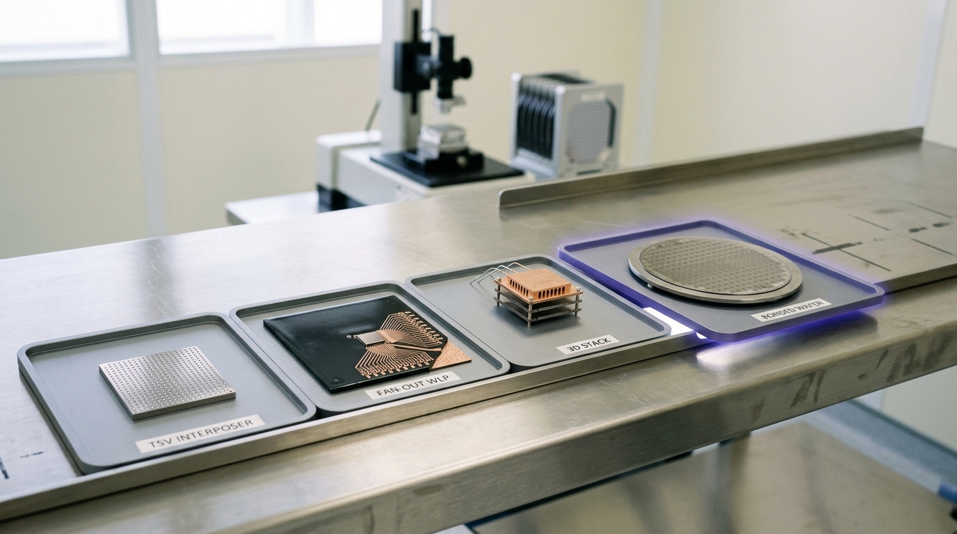
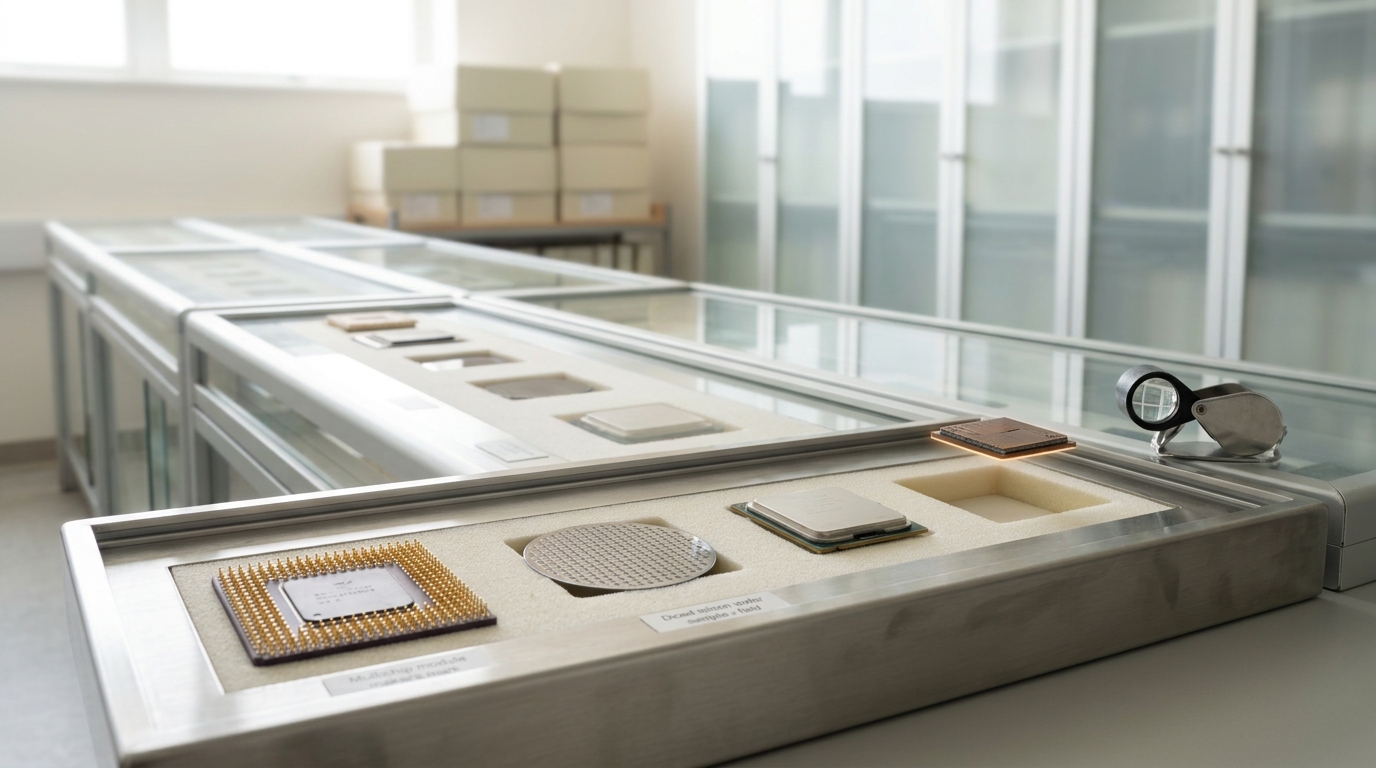
A specimen case holding one artifact from each of four decades makes an argument that no single product announcement can: the multi-die package current accelerators depend on is not a recent invention but a return, made under better economics, to something the industry already knew how to build in 1980 and already knew, by the mid-1990s, was too expensive to build at volume. What changed between the 1990s and the 2010s was not the core idea. It was the through-silicon via and the silicon interposer giving the industry a cheaper physical substrate, and defect densities and die sizes at the leading edge finally crossing the threshold where multiplying good die outweighed the cost of testing and assembling them. UCIe’s 2022 founding is the most recent entry in that record, not its conclusion: a shared electrical and protocol answer to a fragmentation problem that ten companies had each spent the previous several years solving separately, at a cost none of them found worth continuing to bear alone.
Read any future advanced-packaging announcement against that sequence rather than in isolation. Ask which part of the recurring trade-off — density, heat, yield, or interoperability — the new development actually moves, on whose stated authority, and by how much relative to what came immediately before it. That is the only comparison the dated record assembled here actually supports.