A monolithic die fails as one thing. A chiplet package fails as a sequence of things that each had to go right independently, in an order that a single slab of silicon never imposed: every die had to test good alone, then survive being bonded, then survive the thermal and mechanical stack built on top of it, then prove it can actually talk to its neighbors at the protocol layer, and only after all of that does the economics of having disaggregated in the first place resolve one way or the other. None of this is visible from a block diagram showing chiplets as clean rectangles wired together. It shows up on a test floor, at a bonder, in a thermal chamber, and on a compliance bench — four gates, each closing off a distinct failure mode, each with its own instrumentation and its own way of being fooled.
This is a practitioner-level walk through those four gates, in the order a package actually passes through them: known-good-die testing before bonding, the mechanics and tolerances of the bond itself, interoperability validation at the protocol layer, thermomechanical co-design across a heterogeneous stack, and the yield and cost arithmetic that ultimately decides whether disaggregating was worth doing at all. Vendor claims are marked as claims. Where a number comes from a measured report rather than a specification target, that distinction is kept explicit, because in packaging the gap between a datasheet pitch and a shipping yield is where most of the real engineering lives.
Gate one: known-good-die testing, before the bonder ever sees the part
The single fact that makes chiplet economics work or fail is whether a bad die can be caught before it is permanently joined to good ones. A monolithic chip either passes final test or it does not, and the cost of a bad one is one die’s worth of silicon. A chiplet package multiplies that die by however many partners it is bonded to — a defect discovered only after assembly destroys the entire stack, not just the offending part. Known-good-die (KGD) testing exists to move that discovery earlier, and the standard framing is blunt about why: with multi-chiplet architectures now standard, KGD testing is described as the mechanism that keeps final assembly yield economically viable at all, because a die that has been rigorously verified before it reaches assembly is the only kind an integrator can afford to bond in bulk [4].
The arithmetic behind that claim is a plain probability composition, and it
is worth writing down because it is the one piece of real math in advanced
packaging that most design reviews skip past. If each of
which is a first-order model — it assumes bonding introduces no additional
defects and that die yields are independent, both of which are simplifications
addressed separately below. Even under this optimistic assumption, four
chiplets each yielding 95% compose to roughly 81% assembly yield, and a
twenty-die stack at the same per-die yield falls to roughly 35% — the
industry’s own framing of why an unscreened stack becomes uneconomical fast
as die count rises [4]. The entire purpose of KGD testing
is to push each
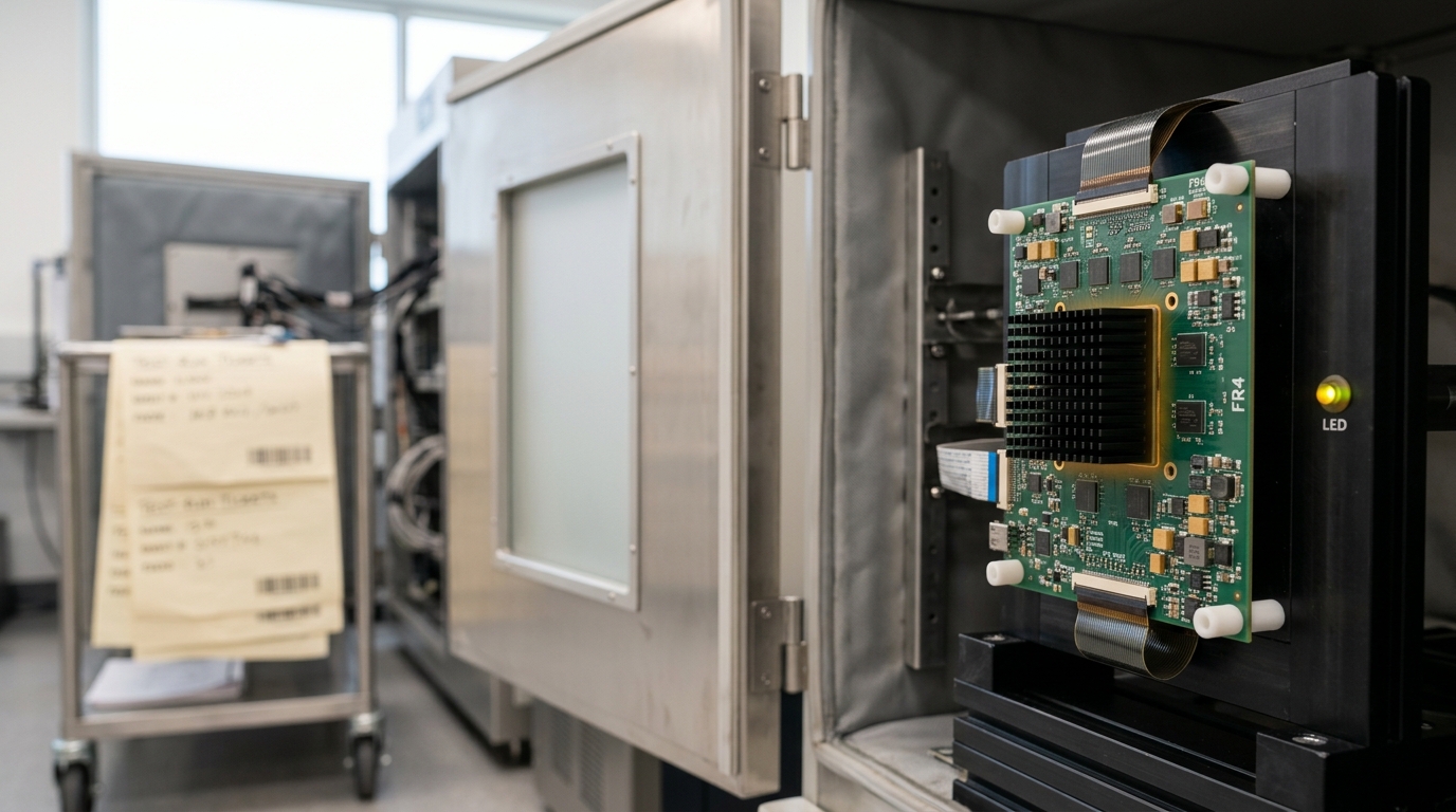
KGD screening itself is not simply “run the same test used for a packaged part on a bare die.” Intel’s own characterization of the practice, cited in an analysis of UCIe-oriented KGD strategy, describes it as total emulation of final packaged test, combined with high thermal stress intended to surface latent defects and high electrical stress to catch marginal parts that would pass a light functional check but fail in the field [5]. That combination — full functional coverage plus deliberate overstress — is what a burn-in chamber is for: a populated test board is run through a temperature ramp specifically to force early-life failures to happen on the bench rather than after bonding, when they cannot be discovered without destroying the package.
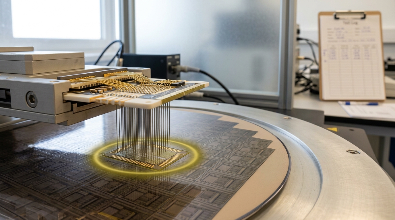
Wafer-level probing of the die is the physical bottleneck in this chain, and it has gotten harder, not easier, as memory and logic chiplets have moved to higher signaling rates. FormFactor’s public description of high-speed KGD wafer test for HBM-class memory dies names two concrete failure modes: at signaling rates above roughly 4 GHz, probe-induced insertion loss starts to degrade voltage swing enough to corrupt the test itself rather than the part under test, and thermal cycling causes coefficient-of-thermal-expansion (CTE) mismatch between the probe card and the wafer, misaligning contact during heated test runs. Their published fix for the second problem — wafer-side stiffeners matched to the probe card’s CTE — reports roughly a 40% alignment improvement, alongside probe-card refinements to reduce thermal scaling error to approximately 65 parts per million [3]. That figure is a vendor-reported result specific to their own hardware, not an industry constant, but it is a useful concrete illustration of how much of KGD testing is really a metrology problem: the test has to remain accurate while the wafer itself is thermally moving under the probe.
Two mechanisms in this practice deserve to be pulled apart, because a review that conflates them will misjudge cost. Electrical test at room temperature catches most manufacturing defects — opens, shorts, gross parametric failures — cheaply and fast. Burn-in catches a different, smaller population: latent defects that pass room-temperature test but fail early in the field under sustained thermal and electrical stress. The two are not substitutes. Skipping burn-in to save test-floor time does not lower the defect rate, it just relocates the failure from the test floor — where it costs one die — to the field, or worse, to the assembled package, where it costs everything bonded to that die.
Gate two: the bond itself, and what its tolerances actually demand
Once a die is screened good, it has to be physically joined to its partners, and the two dominant joining approaches — 2.5D integration through a passive interposer, and 3D hybrid bonding directly between active dies — impose very different tolerance and thermal regimes.
2.5D integration places chiplets side by side on a silicon (or increasingly organic or glass) interposer that carries fine-pitch routing between them and coarser routing down to the package substrate. TSMC’s CoWoS family is the production example most cited in industry coverage: the company has stated it is expanding CoWoS and SoIC advanced-packaging capacity substantially through 2026 in response to AI accelerator demand, a capacity build-out reported publicly as tied to 18 new fabs and advanced-packaging facilities [2]. That is a reported capacity claim, not an independently audited figure, and the underlying article is paywalled beyond its headline statement — worth flagging as a limit on how much can be verified from it, versus how much is simply TSMC’s own disclosure repeated by press.
3D hybrid bonding instead joins two dies (or a die and a wafer) directly, copper pad to copper pad and dielectric to dielectric, with no solder and no intervening bump. The pitch achievable this way is what makes it categorically different from bump-based stacking: Intel’s Foveros Direct 3D began at a roughly 9-micron bond pitch in its first generation, moving toward pitches below 5 microns and a stated second-generation target near 3 microns, a step down by roughly an order of magnitude from the 36-micron microbump pitch used in Foveros’s earlier bump-based 2.5D variant. This is Intel’s own technology disclosure, not an independently measured third-party result, and it should be read as a vendor roadmap claim rather than a shipping-part guarantee for every SKU built on it.
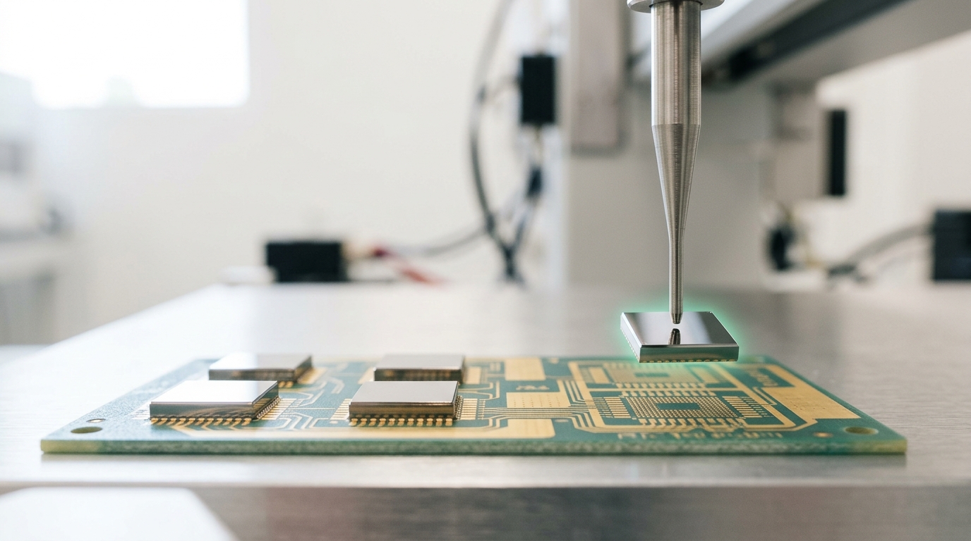
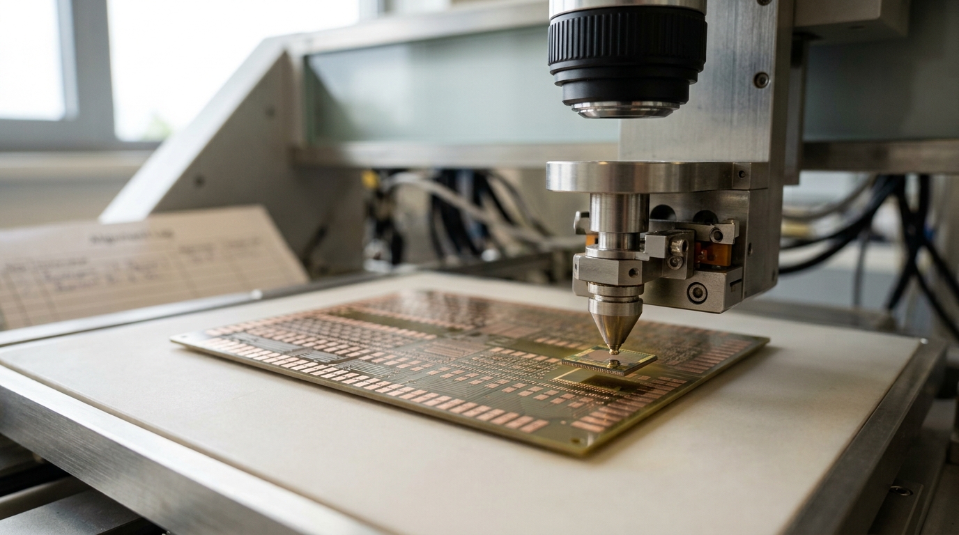
That order-of-magnitude pitch reduction is not free. Hybrid bonding demands sub-micron die-to-die alignment and requires both bonding surfaces to be planarized to a tolerance the bonder’s optics can actually resolve — misalignment or surface roughness that a microbump process would simply absorb in solder reflow has nowhere to go in a direct copper-to-copper joint. This is why bonder qualification includes a split-field microscope check of fiducial alignment before the pick-head ever lowers the die to contact: the alignment has to be confirmed correct before the bond is made, because unlike solder reflow, a hybrid bond is not self-correcting.
Gate three: interoperability, proven on a bench, not assumed from a spec
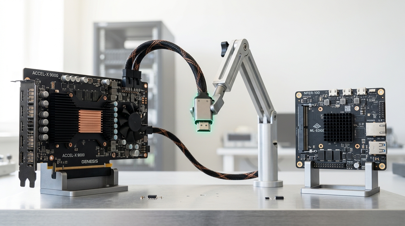
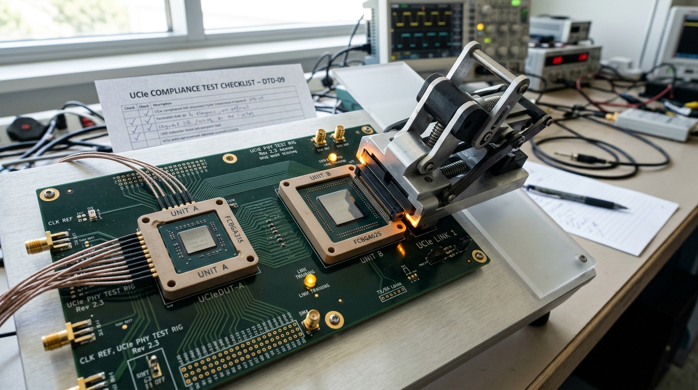
Disaggregation only pays off commercially if chiplets from different design teams — sometimes different companies entirely — can be combined on one package. That promise depends on a shared die-to-die interconnect standard, and Universal Chiplet Interconnect Express (UCIe) is the industry’s open attempt at one. The UCIe specification defines a complete stack: physical layer, protocol layer, software model, and — critically for the practice described here — a defined compliance-testing methodology meant to let a multi-vendor ecosystem actually interoperate rather than merely claim to [1].
The physical-layer numbers matter for what they constrain. UCIe 2.0 supports bump pitches spanning roughly 25 microns down to below 1 micron, covering everything from coarse 2D/2.5D bump-based integration up to the fine pitches hybrid bonding enables, and UCIe 2.0’s per-lane data rate of 32 GT/s has since been extended by UCIe 3.0 to 48 and 64 GT/s — a doubling of per-generation bandwidth [1]. These are specification targets, the maximums a compliant implementation is permitted to claim, not a guarantee that any two vendors’ silicon will interoperate at that rate on first contact.
That gap between “spec-compliant” and “actually interoperates” is exactly what a compliance bench exists to close. Two chiplets built by different teams to the same UCIe physical-layer spec can still fail to link — clock tuning, calibration sequencing, and protocol-layer negotiation all have enough implementation latitude that link training genuinely can fail on a first attempt even between two parts that each individually pass their own spec compliance test. This is why UCIe’s own documentation treats compliance testing as a first-class deliverable of the specification rather than an afterthought left to integrators [1]: without a standardized bench-level interoperability test, “UCIe-compliant” would be a claim about each part in isolation, not a claim about the pair.
Gate four: thermomechanical co-design under a stack that never behaves like one material
A heterogeneous package stacks dies, interposers, and substrates made of different materials with different coefficients of thermal expansion, and that CTE mismatch is the physical root of most advanced-packaging reliability failures. A peer-reviewed review of thermal management in 2.5D and 3D chiplet integration frames the core problem plainly: stacked and laterally integrated dies now generate hundreds of watts per package, producing localized hotspots and inconsistent temperature fields across the stack rather than the roughly uniform temperature a single monolithic die presents [6]. A monolithic die’s thermal design is governed by one material’s expansion behavior; a chiplet stack’s is governed by however many different materials happen to be adjacent at each interface, and the differential expansion between them produces interfacial shear and normal stresses under every thermal cycle the package experiences in operation.
Silicon interposers make this concrete. UCLA’s NanoCAD Lab work on embedded thermal isolators for 2.5D systems treats the interposer as doing double duty — it is simultaneously the electrical redistribution layer between chiplets and a lateral thermal-spreading plane, meaning a routing decision made for signal integrity has thermal consequences, and a thermal decision made to isolate a hot chiplet from a cool one has electrical routing consequences [7]. Warpage driven by CTE mismatch between the silicon interposer and the organic substrate beneath it is commonly controlled in production to within roughly 40 microns using substrate design features such as coreless construction with slits around the interposer — a widely cited mitigation, though the specific tolerance achieved is process- and design-dependent rather than a universal constant.
Finite-element and machine-learning-assisted co-design methods have become the practical way to explore this coupled electro-thermal-mechanical design space, because closed-form models cannot capture the interaction between routing-driven power density, interposer material choice, and resulting warpage cheaply enough to iterate a real design against. Published work on thermo-mechanical co-design of 2.5D flip-chip packages using both silicon and glass interposers frames the problem exactly this way: warpage, stress, and thermal performance have to be co-optimized rather than solved in sequence, because each variable moves the others [8]. This is analysis and methodology description, not a specific product result — worth stating plainly, since it is easy to over-read a co-design paper as evidence about any one shipping package.
None of this modeling substitutes for a measurement taken on the finished part. Warpage predicted at the design stage still has to be confirmed after the package is actually built and has gone through reflow, because the model’s assumptions about material properties, cure shrinkage, and process variation are themselves uncertain. A white-light interferometer scan of the finished package lid is the bench-level check that closes this loop — producing a fringe map of actual surface deviation rather than a simulated one, which is the only way to confirm the stack-up behaved the way the co-design model predicted it would.

Closing the loop: whether disaggregation was worth it
All three preceding gates exist to make one number defensible: the actual yield and cost of the assembled package, compared honestly against what a monolithic die attempting the same function would have cost. That comparison is where chiplet disaggregation is often oversold, because the naive pitch — “smaller dies yield better, so chiplets are always cheaper” — ignores the denominator. Bonding, KGD screening, burn-in, and interposer or substrate cost are all additive expenses a monolithic die never incurs, and they have to be paid for every package, not amortized once.
The yield model above is the honest starting point for that comparison, and
its assumptions matter more than its output. It assumes each die’s yield is
independent of the others bonded alongside it, which is optimistic — a
bonding-process defect (misalignment, contamination, a warped interposer) can
degrade several dies on one assembly simultaneously, correlating what the
simple product model treats as independent draws. It also ignores that bond
yield itself is a separate term: even with every input die screened good, the
bonding step introduces its own defect rate that a pure per-die KGD program
does nothing to fix. A more complete model multiplies the per-die yield
product by a separate assembly yield term, and it is that assembly-yield
term — not per-die screening — that improves as bonder alignment tolerance,
planarization quality, and interposer warpage control mature. This is why the
practice described across the preceding three gates functions as one system:
tightening KGD screening raises the
Memory bandwidth economics illustrate the other side of the ledger: why disaggregation is chosen at all despite this added cost. Coverage of HBM3E’s bandwidth roadmap frames the appeal directly — stacking memory dies via through-silicon vias onto a shared interposer next to a compute die delivers bandwidth per package that a single monolithic die reaching the same memory capacity could not achieve at any reasonable cost or yield, because the pin count and die area a monolithic approach would require scales far worse than the stacked alternative [9]. That is the actual trade being made: added assembly cost and yield risk, purchased in exchange for a bandwidth-per-package or heterogeneity-per-package outcome that no monolithic die at any yield could deliver at all. The economics only clear when that traded-for capability is worth more than the disaggregation tax — which is a design-specific judgment, not a general law favoring chiplets over monolithic integration in every case.

What a review of any specific package should actually ask
Reduced to a checklist, the practice above resolves into five concrete
questions that separate a package that will ship reliably from one that
merely simulated well. First, what KGD screening — electrical and thermal —
was each chiplet actually run through, and at what confidence does that
screening estimate its
A specification sheet, a roadmap slide, or a simulation result can answer none of these five questions definitively on its own. Each requires a measurement taken on real, physically bonded hardware, which is the throughline of every gate described here: known-good-die testing, hybrid bonding and interposer assembly, UCIe interoperability validation, and thermomechanical co-design all exist because a heterogeneous package’s actual behavior is not fully predictable from any one component’s data sheet — it has to be verified as an assembled system, at every gate, before it is allowed to ship.