The step after the foundry, before the customer
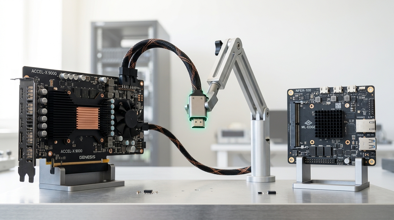
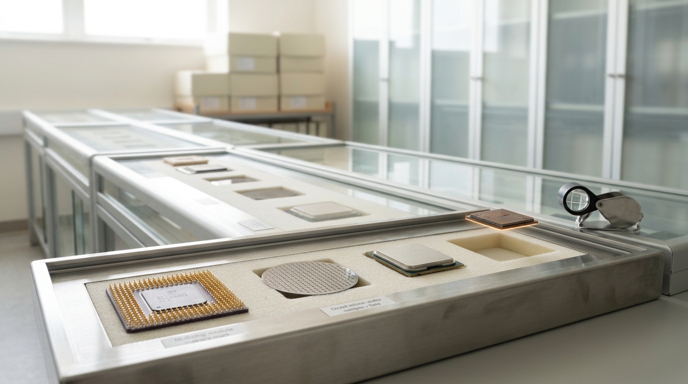
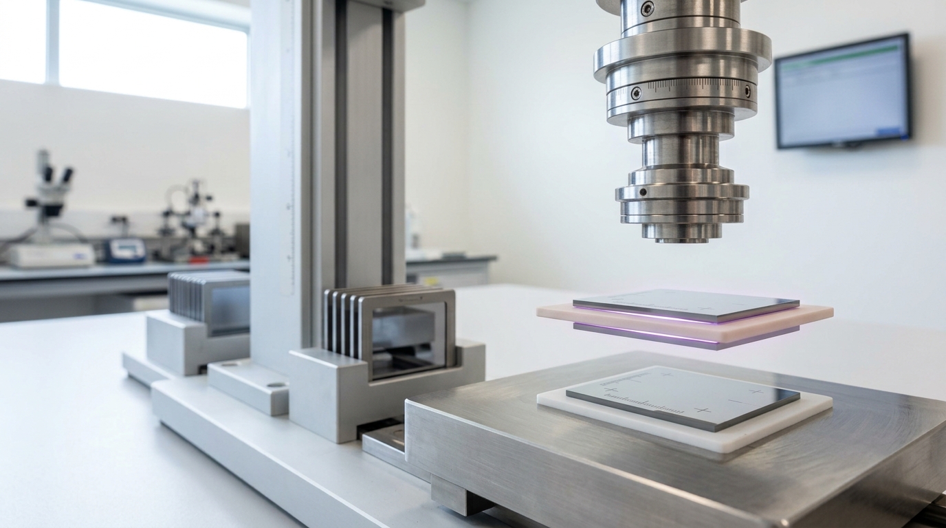
This cohort’s foundry-track briefings end with TSMC, Samsung, or Intel producing a finished, patterned wafer. That wafer is not yet a sellable product. It has to be diced into individual dies, packaged onto a substrate with the connectors a customer’s board actually needs, and tested to confirm it works — a distinct business called outsourced semiconductor assembly and test (OSAT). ASE Technology is the largest company in that business, holding $18.54 billion in reported revenue and a 44.6% share among the top 10 advanced-packaging players combined [1].
Why “the final 25%” undersells the job
Describing OSAT as merely the “final step” understates how much of a modern chip’s actual performance and reliability depends on packaging quality. This cohort’s advanced-packaging and CoWoS briefings establish that packaging capacity, not wafer starts, is the binding 2026 constraint on AI accelerator output — meaning the OSAT layer ASE operates in is not a peripheral finishing touch but one of the industry’s most consequential current bottlenecks [3]. A die that emerges perfectly from TSMC’s most advanced node still cannot reach a customer without passing through a company like ASE first.
Why TSMC increasingly does some of this work itself
TSMC’s own CoWoS advanced-packaging capability, covered extensively in this cohort’s foundry track, represents the foundry taking on packaging work that would traditionally have gone entirely to an OSAT like ASE. That overlap creates a genuinely interesting competitive dynamic: ASE is simultaneously a critical supplier to the broader chip industry and, in the specific advanced-packaging segment TSMC has entered directly, a partial competitor to one of its own industry’s most powerful players [2].
The chiplet trend’s direct effect on ASE’s business
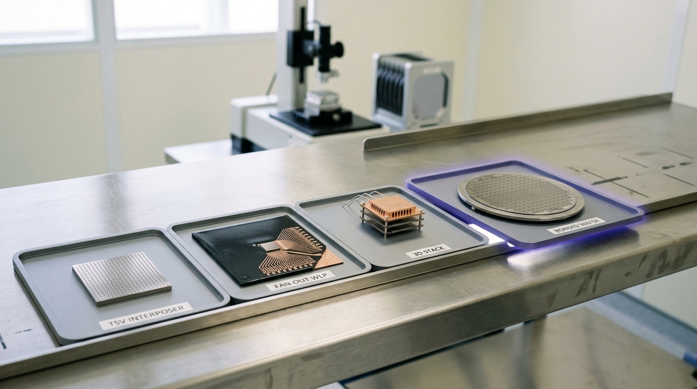
As chip designs increasingly shift toward chiplet-based, heterogeneously integrated packages — the trend covered in this cohort’s dedicated chiplet-economics briefing — the packaging step ASE performs becomes proportionally more complex and more valuable. Fan-out wafer-level packaging, 2.5D interposer integration, and HBM stacking collectively grew from roughly 15% of OSAT revenue in 2020 to an estimated 25-30% by 2026, the clearest single number for how much packaging is “eating” the industry’s growth relative to simpler, traditional packaging methods [4].
Why ASE deserves to be named alongside the chip vendors it serves
Every accelerator, every custom ASIC, and nearly every advanced logic chip covered across this cohort’s other tracks passes through an OSAT like ASE before it becomes a sellable product. That makes ASE’s own capacity, yield, and technology roadmap just as consequential to whether those chips actually reach customers on schedule as the chip designer’s own execution — a dependency this cohort’s packaging-focused briefings argue deserves far more attention than the OSAT layer typically receives in mainstream AI hardware coverage.
What sets ASE apart from a pure contract manufacturer
Unlike a simple contract assembler, ASE’s role increasingly involves genuine engineering collaboration with its customers on package design itself — how a multi-die product is partitioned, how thermal and electrical constraints shape the physical layout, and how the final package interfaces with a customer’s board. That collaborative, engineering-intensive relationship is a meaningful part of why ASE commands the scale and margin it does relative to lower-value assembly work elsewhere in the electronics industry, and why its customer relationships tend to be durable rather than easily switched on price alone.
Taiwan’s dual concentration, worth naming directly
ASE, like TSMC, is headquartered in Taiwan — meaning the island holds a concentrated position at both the wafer-fabrication layer, covered extensively in this cohort’s foundry track, and the advanced-packaging layer this briefing covers. That double concentration is a meaningful, if under-discussed, dimension of the same geographic risk this cohort’s TSMC Arizona briefing frames primarily around fabrication alone — a genuinely complete assessment of supply-chain geographic risk needs to weigh the packaging layer’s concentration in Taiwan alongside the fabrication layer’s, not treat the two as independent risks. This is precisely the gap Amkor’s Arizona campus, covered in this cohort’s companion briefing, is built to address — a domestic packaging option that reduces dependence on ASE’s own Taiwan-concentrated capacity for at least a portion of US-bound advanced chip volume, even as ASE itself remains, by a wide margin, the larger and more established company in the segment as a whole.