A ten-year bet on where the seam goes, made explicit
Ask a packaging engineer where advanced packaging will stand in 2035 and the honest answer is a distribution over outcomes, not a point estimate. This article builds that distribution in public, using one discipline throughout: every claim below is tagged as a fact (measured, disclosed, and citable), a vendor claim (a company’s or consortium’s own assertion about its own technology, reported as such and not endorsed), an analysis (a structural argument built from disclosed numbers), a scenario (one internally consistent path the evidence permits, not the one this article expects), or a prediction (a specific, dated, falsifiable claim with the observation that would prove it wrong stated in advance). Where the people building this technology disagree, that disagreement is described rather than resolved in one direction, and no cross-vendor ranking is built from any single company’s own reported numbers about its own product.
A companion piece in this publication, “When the Substrate Became the Product,” worked through why the package displaced the die as the unit of design and treated energy per bit as a function of distance as the throughline connecting reticle limits, chiplet interfaces, 2.5D proximity, 3D stacking and yield. This piece does not repeat that account. It takes the state that piece described as of 2026 and asks, trajectory by trajectory, what a decade of further motion looks like — and states in advance what observation would prove each extrapolation wrong.
Five trajectories organise what follows: whether the Universal Chiplet Interconnect Express standard (UCIe) achieves broad, plug-and-play cross-vendor interoperability or stays a standard vendors use bilaterally without ever building an open marketplace on it; how far hybrid-bonding pitch keeps halving on its demonstrated schedule; whether 3D stacking becomes the default over 2.5D integration for AI-accelerator logic specifically, not only for memory, where it already is the default; whether packaging and substrate capacity can be built out fast enough to meet demand rather than trailing it; and what could force a discontinuity in any of the above, from an alternative bonding chemistry to optical interconnects integrated at the package boundary.
The documented present
Fact. The UCIe consortium’s own specification history runs through four public releases. UCIe 1.0 defined the die-to-die physical layer, protocol stack and a compliance programme; 1.1 stayed fully backward compatible while adding runtime health monitoring and lower-cost packaging options; 2.0 added manageability and a debug architecture, and extended the standard to 3D packaging with a physical layer specified for bump pitches “as big as 10-25 microns to as small as 1 micron or less”; 3.0, released in the second half of 2025, doubled the top data rate from 32 to 48 and 64 giga-transfers per second for both standard-package (UCIe-S) and advanced-package (UCIe-A) links, extended sideband reach to 100 millimetres, and added runtime transmitter-side recalibration, while remaining backward compatible with everything before it [1, 2].
Fact. At Chiplet Summit 2026, Intel and Cadence connected independently designed chiplets implementing 16 gigatransfer-per-second UCIe-S physical-layer intellectual property on a shared “Cameron Creek” test chip. The consortium’s own account of the event describes it as “the industry’s first live UCIe-S interoperability demonstration,” stating that it “validated true cross-vendor interoperability and successful UCIe Interoperability Testing” [3]. That is the standard-setting body’s characterisation of its own ecosystem’s progress, made by an organisation with an obvious interest in the answer, and this article treats it as exactly that — a documented event, reported by an interested party, rather than an independently audited claim.
Fact. On the bonding side, imec and EV Group demonstrated wafer-to-wafer hybrid bonding at a 200-nanometre copper interconnect pitch in May 2026, achieving a copper pad-to-pad post-bond overlay vector below 40 nanometres for 100 percent of dies across a full 300-millimetre wafer — a result imec’s press release describes as a world first — following an earlier published milestone at 400-nanometre pitch [4]. imec’s Zsolt Tokei is quoted stating the intent to “drive the roadmap well below 200nm interconnect pitch to unlock the most demanding logic-to-logic and memory-to-logic stacking use cases” [4]. Two years earlier, imec’s own published roadmap had already named 400 and 200 nanometres as forecast wafer-to-wafer targets, alongside microbump pitches in industrial use between 50 and 30 micrometres and imec’s own targets of 10 and 5 micrometres for finer bumping [5]. The 2026 result landed on a target the 2024 roadmap had already set, which is a modest but real form of corroboration: the forecast and the achievement agree.
Trajectory one: does UCIe converge on real interoperability, or stay bilateral?
Analysis. A specification and an interoperable market are not the same achievement, and the gap between them is where this trajectory’s real uncertainty sits. Beyne and Van der Plas, describing the physical menu of bonding and bumping options available today, characterise the choice among them explicitly as “a trade-off between cost, pitch, compatibility, and interoperability” [5] — a framing that treats interoperability as one design variable among several rather than a solved precondition. The Intel-Cadence demonstration proves something real and specific: that two independently designed physical-layer implementations, from two different companies, can be wired together and pass traffic without custom adaptation logic at the electrical layer [3]. It does not by itself prove that a buyer can select chiplets from an open catalogue the way a systems integrator selects rack components today, because a working PHY-layer link is only one layer of what a shipping multi-die product needs.
That gap is visible in the packaging discipline immediately adjacent to UCIe. Brett Wilkerson of AMD, discussing the need to integrate third-party chiplets via hybrid bonding at the IEEE Electronics Packaging Society’s summary of the 2025 ECTC special session on hybrid bonding, described chiplet modules as complex and noted that hybrid-bond intellectual-property standards — a shared Library Exchange Format for through-silicon vias and copper bumps, routing guidelines, input/output specifications and validation, design-rule and layout-versus-schematic checking, and electromigration and IR-drop verification tools spanning multiple systems-on-chip — are still needed before third-party hybrid-bonded integration becomes routine, and that “with HB the time-to-market concerns become one of the limiting factors in adoption” [12]. An open electrical standard at the die-to-die interface and an open design-tooling standard for the physical bond that carries it are two different problems, and as of 2026 only the first has a live, demonstrated cross-vendor result.
Ecosystem breadth is a separate and more encouraging signal. The consortium reports that UCIe 3.0 won the Chiplet Summit’s Best in Show award for connectivity and interoperability, and lists sponsor and exhibitor participation from Arm, Marvell, Synopsys, Siemens, Eliyan, Alphawave Semi, Keysight Technologies, Tenstorrent, and several smaller chiplet and test-equipment vendors alongside Intel and Cadence [3]. Breadth of participation is a leading indicator of a standard gaining traction; it is not itself proof that traction converts into a marketplace where dies from unrelated vendors ship together in volume products.
Prediction. Horizon: end of 2030. Assumption: no single vendor’s proprietary die-to-die interface displaces UCIe as the reference standard used in public interoperability demonstrations. Indicator: the number and character of publicly documented, third-party-verified cross-vendor UCIe interoperability demonstrations, and whether any shipping commercial product combines dies from two unrelated design houses over an unmodified UCIe link. Disconfirmed if, by the horizon, either no additional cross-vendor UCIe interoperability demonstration beyond the 2026 event has been publicly documented, or a shipping commercial multi-die product has combined dies from two unrelated vendors over UCIe without vendor-specific adaptation — the first would show the standard stalling, the second would show it has already succeeded well ahead of this horizon.
Trajectory two: how far does bond pitch keep halving?
Analysis. The physical reason pitch matters this much is a simple scaling relationship worth making explicit. For interconnects arranged on a roughly square grid at pitch
Halving the pitch is therefore not a doubling of available interconnect density; it is close to a quadrupling. That is the assumption doing the work every time a packaging roadmap reports a pitch number: the 2024-to-2026 move from 400 to 200 nanometres in imec and EV Group’s demonstrated wafer-to-wafer results is not a twofold gain in what a fixed bonding area can carry, it is closer to a fourfold one [5, 4]. The comparison across bonding technologies published in the IEEE Electronics Packaging Society’s summary of the 2025 ECTC hybrid-bonding session makes the same point at a coarser grain: reported bump pitch runs above 130 micrometres for solder bump, 90 to 130 micrometres for copper pillar, 20 to 50 micrometres for microbump, and below 10 micrometres for hybrid bond, with defect sensitivity tightening from above 10 micrometres for solder bump to 0.15 to 0.5 micrometres for hybrid bond, and overlay and alignment error tightening from above 10 micrometres to 0.05 to 0.25 micrometres over the same progression [12]. Each step down in pitch buys interconnect density at a steep, non-linear rate — and demands alignment precision that tightens at close to the same rate.
That second half of the trade is where yield risk concentrates. If a bonded interface carries
Because
Fact. Samsung’s SuJin Ahn, presenting at the same 2025 ECTC session, identified particle monitoring and control, and warpage control for larger and thinner dies used in AI applications, as the two main near-term challenges for hybrid bonding, stating that die warpage must be contained to within roughly 100 nanometres for successful stacking, and citing a Yole Group finding of an 18 percent compound annual growth rate projected for hybrid-bonding technology products against a 13 percent rate for advanced packaging overall through 2029 [12]. Separately, a June 2026 paper submitted to the IEEE 76th Electronic Components and Technology Conference reports a pneumatic wafer-warping technique for fusion bonding that applies uniform backside pressure rather than a localised bonding force, achieving sub-10-nanometre residual grid distortion with basic correction and 3 nanometres or below with more advanced correction — a result the authors position as relevant to the backside power-delivery networks that logic-on-logic stacking will require [10]. Both results describe engineering responses to the same underlying constraint: finer pitch is available in the laboratory, but converting it into shippable yield at scale is its own, still-developing discipline.
Prediction. Horizon: end of 2031. Wafer-to-wafer hybrid-bonding pitch in published, credible roadmap or demonstration results will continue to move below the 200-nanometre level already reached in 2026, without a change in the underlying copper-to-copper direct-bonding approach. Assumption: yield-modelling and warpage-control techniques such as YAP±style simulation and pneumatic or otherwise compliant bonding continue converting demonstrated pitch into usable yield fast enough to make each further step commercially attractive rather than merely a laboratory record. Indicator: the pitch and paired overlay-accuracy figures disclosed in imec’s, EV Group’s, and major foundries’ published wafer-to-wafer bonding results. Disconfirmed if, by the horizon, no publicly reported wafer-to-wafer result has moved past the 200-nanometre pitch achieved in 2026, or a materially different bonding chemistry has displaced direct copper-to-copper hybrid bonding as the leading approach for logic-class stacking.
Trajectory three: does 3D stacking become the default over 2.5D?
Fact. imec’s Anne Jourdain, at the same ECTC session, described three distinct hybrid-bonding integration scenarios at different points on the maturity curve: wafer-to-wafer bonding, already in production for memory-on-memory stacking; die-to-wafer bonding, progressing quickly toward enabling logic-on-memory and logic-on-logic stacking; and die-to-die bonding, still emerging, aimed at chiplet architectures and repair functions. She stated that achieving tight pitch requires not only extreme alignment accuracy — below 50 nanometres — but also process stability across large areas, with copper protrusion control and dielectric planarisation as key enablers [12]. That ordering matters for this trajectory specifically: 3D stacking is already the default for memory. Whether it becomes the default for the hot, high-power logic dies in an AI accelerator is a materially different and still open question.
Analysis. The physical case for extending 3D past memory is straightforward and is the same case advanced elsewhere in this publication’s coverage of energy per bit: vertical hybrid-bond interconnects at sub-micrometre pitch have a reach so short that the distance term in a link’s energy cost nearly disappears, and Wilkerson’s own interconnect-density comparison, presented at the same session, ordered five packaging approaches — two-dimensional multi-chip modules, 2.5D silicon-interposer and elevated fan-out bridge integration, high-bandwidth memory, on-die cache, and 3D chiplets — by both linear and areal interconnect density, with 3D chiplets reaching the highest density on both axes [12]. On density alone, 3D wins by a wide margin over any 2.5D arrangement.
Analysis. The countervailing case is thermal and organisational, not electrical. Wilkerson pointed out that 3D stacking inherently raises thermal-dissipation difficulty, that hybrid- and fusion-bonding films increase thermal resistance directly in the critical heat path, and that designers need transient rather than only steady-state thermal analysis to build thermally robust stacked systems [12]. Samsung’s warpage findings point the same direction from a different angle: warpage increases specifically with the large, thin dies that high-performance AI logic tends to use, and the roughly 100-nanometre containment threshold for successful stacking is a tight tolerance to hold at the reticle-scale die areas accelerator logic favours [12]. Layered on top of both is the design-tooling gap described in trajectory one: the hybrid-bond intellectual-property standards Wilkerson called necessary for third-party integration do not yet exist in mature form [12]. Three genuinely independent constraints — thermal, mechanical, and organisational — all sit on the same side of the ledger against logic-class 3D stacking, while only interconnect density argues for it. That asymmetry is itself informative: it suggests the transition, if it happens, will be gated less by any single breakthrough than by whether all three constraints loosen roughly together.
Prediction. Horizon: end of 2032. Die-to-wafer or die-to-die hybrid bonding will be in commercial production use for logic-on-logic stacking in at least one shipping AI-accelerator product line, but 2.5D integration (interposer- or bridge-based, without vertical logic-on-logic bonding) will remain the majority approach for high-performance AI-accelerator logic dies by shipment volume. Assumption: transient thermal management and hybrid-bond design tooling for third-party logic integration both improve enough to reach production use for at least one vendor, without improving so fast or so broadly that they overtake 2.5D as the majority approach industry-wide within the horizon. Indicator: vendor product disclosures specifying whether accelerator logic dies are 2.5D-interposed or vertically hybrid-bonded, and disclosed transient thermal design methodology in packaging conference papers. Disconfirmed if, by the horizon, no shipping AI accelerator uses hybrid-bonded logic-on-logic stacking at all, or logic-on-logic hybrid bonding has already become the majority approach for high-performance accelerator logic.
Trajectory four: can capacity keep pace with demand?
Fact. TrendForce reported in April 2026, citing institutional investors, that TSMC’s CoWoS advanced-packaging capacity was projected to reach roughly 115,000 to 140,000 wafers per month by the end of 2026 and approximately 170,000 wafers per month in 2027, with expansion concentrated at the company’s Tainan and Chiayi sites, alongside a panel-level packaging effort (CoPoS) whose pilot line completed major equipment installation in February 2026 with full-line setup expected by mid-2026 and mass production anticipated in 2028 to 2029 [8]. Vendor claim. TSMC’s own chairman is reported in the same coverage stating the company offers “the industry’s largest reticle-size packaging solutions” in the context of competition from Intel’s EMIB technology [8] — a comparative claim made by an interested executive, reported here as exactly that.
Fact. Intel’s own newsroom account, published in July 2026, states that advanced packaging technologies are “expanding the ‘reticle limit’ — scaling packages to 8x the industry standard today, and over 12x by 2028,” and describes its Rio Rancho, New Mexico advanced-packaging facility as employing 2,700 people and engaging 500 suppliers [7]. Both companies’ figures describe their own facilities and are not independently audited; what is independently verifiable is that both are simultaneously and publicly committing capital to the same constraint at the same time, which is itself a fact about the industry’s shared assessment of where the bottleneck sits.
Analysis. Samsung’s citation of Yole’s 13 percent compound annual growth projection for advanced packaging overall through 2029, against an 18 percent rate specifically for hybrid-bonding products [12], is consistent with the capacity build-out both foundries are reporting: hybrid bonding is growing from a smaller base but faster than advanced packaging as a whole, which is exactly the pattern a genuinely newer, still-scaling process technology should show relative to the more mature CoWoS-style interposer packaging it is layered alongside rather than simply replacing.
Prediction. Horizon: end of 2029. Reported advanced-packaging capacity growth (CoWoS-class 2.5D and SoIC-class 3D combined, across TSMC, Intel, and Samsung) will continue to be reported by industry analysts as running behind disclosed or inferred demand for AI-accelerator packaging, rather than converging with it. Assumption: AI-accelerator unit demand continues growing at a pace comparable to 2024-2026 rates, and no major demand-side correction removes the pressure driving current capacity announcements. Indicator: continued industry-analyst reporting of a supply-demand gap specifically in advanced packaging, distinct from wafer-fabrication capacity. Disconfirmed if, by the horizon, credible industry reporting describes advanced-packaging utilisation at or below wafer-fabrication utilisation for four consecutive quarters, indicating the gap has closed.
Trajectory five: what could force a discontinuity
Vendor claim. Toray’s Masao Tomikawa, presenting the company’s polymer hybrid-bonding work at the 2025 ECTC session, described drawbacks of conventional inorganic silicon-dioxide hybrid bonding for chip-to-wafer applications: sensitivity to particles, high thermal stress from annealing above 350 degrees Celsius, and process-induced warpage severe enough to damage high-bandwidth-memory stacks. Toray’s proposed alternative uses polyimide-based polymer dielectrics bonded below 250 degrees Celsius and under reduced pressure, offering a wide coefficient-of-thermal-expansion tuning range of roughly 5 to 100 parts per million per kelvin, greater particle tolerance, and reduced mechanical stress; Tomikawa reported bonding trials achieving high-yield polyimide-to-silicon-dioxide bonds with alignment accuracy below 2 micrometres and reliable electrical-resistance measurements, and stated the approach is compatible with glass substrates and existing wet-based deposition tooling [12]. This is a company describing its own proposed alternative to the dominant bonding chemistry, not an independently validated industry transition, and the honest reading is narrower than “polymer bonding is coming”: it is that at least one credible materials supplier has built a working case that the industry’s current inorganic hybrid-bonding chemistry is not the only physically viable path to fine-pitch bonding, particularly where glass substrates or panel-level processing are involved.
Vendor claim. A second, electrically rather than materially framed candidate for discontinuity comes from Ayar Labs, which frames the Universal Chiplet Interconnect Express standard as infrastructure for optical, not only electrical, die-to-die communication: the company states that copper reach inside a package tops out around 25 millimetres on an organic substrate, while UCIe-compliant optical retimers built around its TeraPHY chiplet can extend reach to “hundreds of meters,” with longer-haul optical links reaching distances up to 2 kilometres, and it claims optical bandwidth density comparable to or better than proprietary electrical interconnects such as NVLink [9]. Analysis. The company’s own framing — that data on copper hits “a traffic signal every few inches” while data on optics runs on “an open, signal-free highway” [9] — is marketing language from a firm that sells optical interconnect silicon, and its bandwidth-density comparison is a claim about its own product relative to a competitor’s, not an independently measured benchmark; both should be read accordingly. What is structurally interesting regardless of whose numbers are used is the shape of the claim: that the boundary between copper and optics is moving inward, from the rack, to the board, toward the package edge itself, which — if it happens — is a different kind of discontinuity from a new bonding chemistry, because it would change what UCIe’s own physical layer needs to physically be rather than only how bonding is done beneath it.
Analysis. These two candidate discontinuities are not competing explanations of the same event; they sit at different layers. A new bonding chemistry, if adopted, changes how dies are physically joined within a package. Optical interconnect integration, if adopted at package scale, changes how signals leave a package at all. Either could occur without the other, and the evidence available in 2026 supports treating both as live but unresolved possibilities rather than as an inevitable roadmap item.
Prediction. Horizon: end of 2030. Neither candidate discontinuity will have become the majority approach in its domain: inorganic copper-to-copper hybrid bonding will remain the dominant fine-pitch bonding chemistry for logic and memory stacking industry-wide, and copper will remain the dominant physical layer for intra-package, board-level die-to-die links, even as polymer bonding and co-packaged optics both continue to gain documented, real but minority commercial use in specific niches (glass or panel-level substrates for the former; rack-scale accelerator interconnect for the latter). Assumption: neither alternative demonstrates a cost or yield advantage decisive enough to trigger a rapid, broad platform switch within the horizon. Indicator: the bonding chemistry and physical interconnect layer disclosed in major vendors’ shipping accelerator packaging specifications. Disconfirmed if, by the horizon, either polymer or another alternative bonding chemistry has become the majority approach for logic-class fine-pitch bonding, or optical interconnects have become the majority physical layer for board-level die-to-die links inside a single accelerator package — either would mark a discontinuity arriving faster than this prediction assumes.
Two axes, four scenarios toward 2035
Crossing trajectory one (UCIe converges toward broad interoperability, or stays largely bilateral) against trajectories two, three and five together (integration keeps scaling smoothly along its demonstrated curve, or a physical or organisational wall forces a discontinuous change in how dies are joined) gives four internally consistent futures. None is named as the likely one; each is stated with the observation that would rule it out.
Scenario A: Open Catalogue, Smooth Curve. UCIe interoperability broadens past bilateral demonstrations into routine, third-party-verified multi-vendor products, the hybrid-bond design-tooling gap Wilkerson described closes, and bond pitch, capacity and thermal management all continue improving along roughly their current curves without a forced platform change. Horizon: a recognisable open, multi-vendor chiplet market by 2032; smoothly continuing physical curves through 2035. Assumptions: hybrid-bond IP standardisation proceeds at a pace comparable to UCIe’s own electrical-layer standardisation; no physical wall forces a bonding-chemistry or interconnect-layer switch. Indicators: shipping products combining dies from unrelated vendors over unmodified UCIe links; continued incremental (not discontinuous) pitch, capacity and thermal disclosures. Disconfirmation: falsified if, by 2032, no shipping product combines unrelated vendors’ dies over UCIe, or if any of the physical trajectories shows a sharp discontinuity rather than continued smooth scaling.
Scenario B: Open Catalogue, Forced Detour. Interoperability broadens as in Scenario A, but a physical wall — a yield ceiling in fine-pitch bonding, a thermal limit on logic-on-logic stacking, or a capacity shortfall that outlasts current build-outs — forces a genuinely new bonding chemistry or interconnect layer into the mainstream at the same time the market opens. Horizon: open catalogue recognisable by 2032; a forced, industry-wide integration change visible within a two-to-three-year window before 2035. Assumptions: whichever physical constraint binds first is shared broadly enough across vendors that the forced change happens roughly together. Indicators: a coordinated shift in disclosed bonding chemistry or interconnect layer across multiple vendors’ flagship packages within the same window, alongside continued interoperability broadening. Disconfirmation: falsified if an open catalogue emerges with no discontinuity in any physical trajectory, or if a forced change happens without the market having opened.
Scenario C: Vertical Silos, Smooth Curve. UCIe remains a standard vendors use for their own internal chiplet mixing and occasional bilateral partnerships rather than an open catalogue — the electrical layer stays compatible while the surrounding design, test and business-model tooling never standardises enough for a stranger’s die to be a routine purchase decision — while bond pitch, capacity and thermal management continue improving smoothly regardless, because none of those curves actually depended on a multi-vendor marketplace existing. Horizon: interoperability recognisably still bilateral through 2032; physical curves continuing smoothly through 2035. Assumptions: the economic value of standardised reuse within one vendor’s own product line is sufficient to keep UCIe adoption growing even without a genuine third-party marketplace. Indicators: continued UCIe adoption in vendor roadmaps with no third-party-verified unrelated-vendor shipping product; steady physical trajectory disclosures. Disconfirmation: falsified if a genuine unrelated-vendor shipping product appears, or if a physical discontinuity occurs despite the market staying closed.
Scenario D: Vertical Silos, Forced Detour. Interoperability stays bilateral as in Scenario C, and a physical wall separately forces a bonding-chemistry or interconnect-layer change — the least coordinated of the four futures, since neither the standardisation pressure nor the physical response is shared broadly across the industry, producing a more fragmented, staggered pattern of vendor-specific responses to vendor-specific constraints. Horizon: bilateral interoperability persisting through 2032; the first vendor-specific forced change recognisable by 2030-2031, without industry-wide convergence by 2035. Assumptions: physical constraints differ enough by vendor’s specific stack choices that no shared, coordinated response emerges. Indicators: forced changes in bonding chemistry or interconnect layer occurring in different years for different vendors, each tied to a vendor-specific disclosed constraint, with no broadening of cross-vendor interoperability alongside them. Disconfirmation: falsified if a forced change is shared across multiple vendors simultaneously (indicating Scenario B instead), or if the market opens despite the forced change (indicating Scenario B or A instead).
What survives across all four cells, and the wildcard none of them names
Three things hold regardless of which cell the evidence eventually favours. First, none of the five trajectories requires an unannounced research breakthrough to keep moving; each has an incremental, engineering-driven path already visible in a published specification, roadmap, or conference result [2, 4, 12]. Second, the tension inside trajectory three — interconnect density favouring 3D stacking against thermal, mechanical and organisational constraints holding it back — is a disagreement about which constraint binds first, not about whether the underlying physics is real; every party at the 2025 ECTC session agreed hybrid bonding delivers density that 2.5D cannot match, and disagreed only on how fast the surrounding problems get solved [12]. Third, no scenario above requires that either of trajectory five’s candidate discontinuities is a mistake; Toray’s polymer chemistry and Ayar Labs’ optical framing remain internally coherent claims about different layers of the same stack, not competing answers to the same question [12, 9].
The blind spot shared by all four scenarios is the same kind a packaging-focused article cannot see from inside packaging: a shift in what AI accelerators are actually computing, large enough to change how much interconnect a system needs relative to how much arithmetic it does. Every trajectory here assumes accelerator workloads keep demanding roughly the same balance of dense local compute and cross-die bandwidth that has driven packaging investment since 2022. A workload shift profound enough to change that balance — architectures needing far less cross-die communication per unit of useful computation, or conversely ones needing dramatically more — would move several of these curves at once in a way none of the four scenarios traces, because all four take the target packaging is being built to hit as roughly fixed. That is a genuine limitation of a packaging-focused article, stated rather than hidden: these are scenarios for how the physical assembly evolves given roughly its current job, not a claim that the job itself stays fixed through 2035.
What to take away
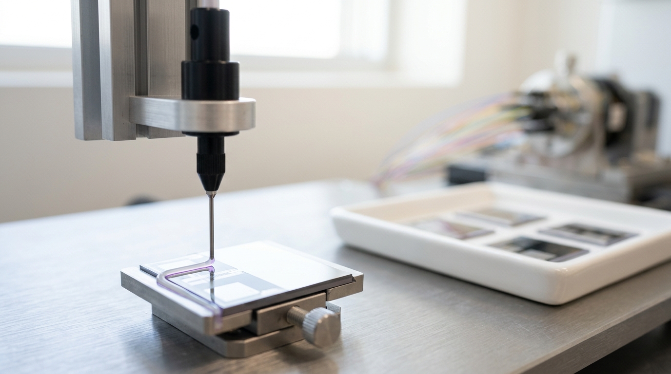
A coupon a fraction of a micrometre from full contact is not yet a bond, and every number in this article’s five trajectories was, at some point, exactly that close and no closer: a pitch demonstrated once on one wafer, a cross-vendor link proven on one test chip, a capacity figure that is a projection rather than a shipped wafer count. Bond pitch has moved from 400 to 200 nanometres in roughly two years, tracking a roadmap set in advance rather than surprising it; two vendors have proven a cross-vendor electrical link works while the design tooling to make that routine still does not exist; and two foundries are pouring capital into packaging capacity at the same time analysts still describe demand as running ahead of it. None of those facts is a forecast of 2035. Each is what is verifiably true in 2026, with the falsifiable claim about where it leads stated separately and in advance.
The more consequential open question is not any single trajectory but which pair of answers the industry lands on: an open catalogue or vertical silos, a smooth curve or a forced detour. That question will not be settled by extrapolating any one curve harder. It will be settled by whether hybrid-bond design tooling standardises as fast as the electrical layer already has, whether thermal and yield engineering keep pace with pitch, and whether a genuinely different bonding chemistry or interconnect layer proves itself outside its current niche before 2035 rather than after it. This article’s four scenarios name that question honestly rather than resolving it in advance, because the record available in 2026 supports all four, and the discipline that matters is not guessing correctly now. It is writing down, for each, what a specific observation between now and 2035 would have to look like to prove it wrong.