The arithmetic behind an industry-wide shift
Chip designs across nearly every company covered in this cohort’s accelerator and foundry tracks have shifted from monolithic scaling — one continuously larger die — toward chiplet-based heterogeneous integration: multiple smaller dies, each individually manufactured and tested, then assembled together on a shared substrate or interposer. This briefing works through the yield economics that make that shift the economically rational choice, not merely an engineering trend.
The core relationship: defects scale with area, yield does not scale linearly
Manufacturing defects on a silicon wafer occur at a roughly constant density per unit area, determined by the maturity of the process node and the cleanliness of the fab. A larger die covers more wafer area, and therefore has a higher probability of containing at least one fatal defect, than a smaller die manufactured on the identical process. Critically, this relationship is not linear — a die twice the area of another is more than twice as likely to contain a defect, because the probability compounds across the larger area. This is the same yield-economics reasoning this cohort’s SMIC briefing applies to explain Huawei’s Ascend 910C’s reported 20-40% yield [5].
The chart above is illustrative — actual yield curves depend on a specific process node’s mature defect density, which varies by fab and generation — but the qualitative shape is well established across the industry: yield degrades sharply, not gradually, as die area grows, which is exactly the pressure pushing designs toward smaller individual pieces.
Why chiplets trade a yield problem for a packaging problem
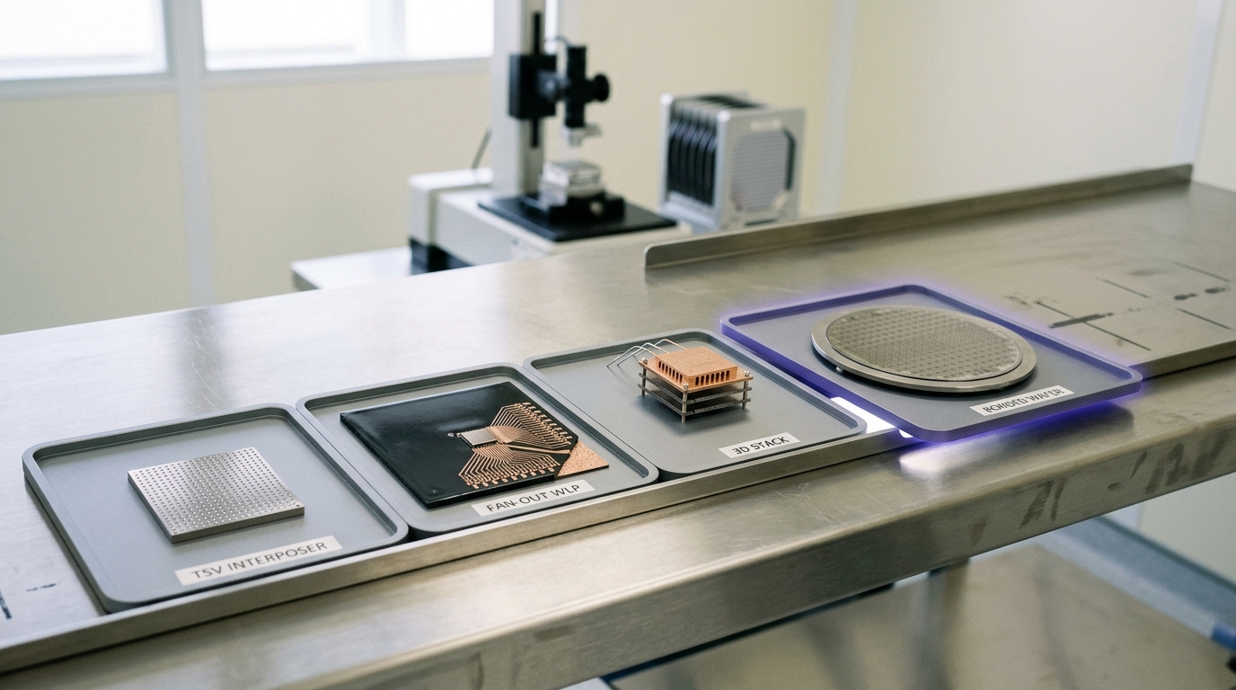
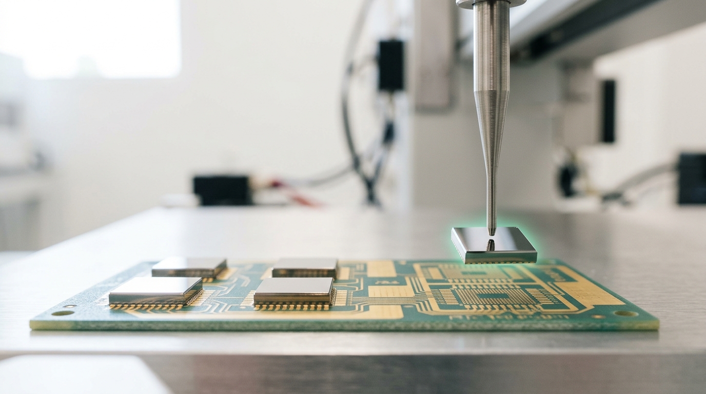
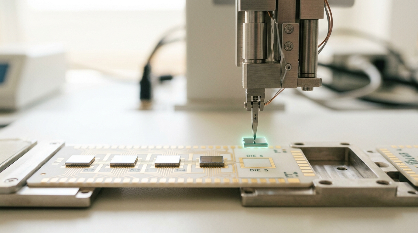
Splitting one large design into several smaller chiplets dramatically improves the yield of each individual piece, since each is manufactured on a much smaller area with a correspondingly lower defect probability. But it does not make the underlying complexity disappear — it moves that complexity to the packaging step, where the individually good chiplets must be precisely aligned, bonded, and interconnected onto a shared substrate or interposer. This is precisely why this cohort’s CoWoS and OSAT briefings identify advanced packaging, not wafer fabrication, as the binding 2026 constraint on AI accelerator supply [1]: the industry collectively traded a yield problem at the wafer-fab layer for a capacity problem at the packaging layer, and packaging capacity has proven harder to scale quickly.
The quantified trade-off, put together
Combining the yield-improvement side with the packaging-cost side gives the actual economic logic: a chiplet approach is worth pursuing when the yield improvement from smaller individual dies outweighs the added packaging cost and complexity of assembling them together. That threshold has moved sharply in chiplets’ favor as process nodes have advanced and defect densities at the leading edge have risen relative to older, more mature nodes — exactly the dynamic behind IDC’s own advanced-packaging market forecast projecting continued strong growth through 2029 [6], and the same dynamic behind the OSAT revenue-share shift documented above [3].
HBM as the clearest, most extreme example of this logic
This cohort’s HBM-supercycle briefing describes memory stacking as its own extreme case of this same trade-off: rather than building one enormous, monolithic memory die — which would carry brutal yield economics at the required capacity — HBM stacks many smaller, individually tested dies vertically, accepting substantial packaging complexity (TSV etch, hybrid bonding) in exchange for yield economics no monolithic approach could match [7].
Why Cerebras is the deliberate exception that proves the rule
This cohort’s Cerebras briefing covers the one major counterexample: wafer-scale integration, which deliberately keeps an entire wafer as one continuous piece rather than dicing it into chiplets at all. Cerebras’s technical achievement is precisely solving the defect-tolerance problem this briefing describes through architectural redundancy — routing around flaws rather than avoiding large-area yield risk by cutting the wafer apart [4]. That Cerebras required years of dedicated architectural innovation to make wafer-scale economically viable, while chiplet-based approaches work with comparatively conventional design techniques, is itself strong evidence for how much yield economics favors the chiplet approach as the default choice industry-wide.