The seam has physics now
When two pieces of silicon are joined into one package, four separate physical acts have to happen, in order, before either piece can do anything useful with the other. A surface has to be prepared and pressed against another surface so that copper touches copper without a drop of solder between them. A hole has to be cut clean through several hundred micrometres of crystalline silicon and then filled solid with a metal that will not crack or void inside it. A carrier wafer of that same silicon has to be turned into a many-layer wiring plane fine enough to fan a die’s bond pads out to something a package can reach. And once all three of those are physically true, the two sides of the new seam have to agree, electrically, on how to talk to each other — because a wire that used to be a few micrometres of on-die metal is now a connection between two objects that were designed separately, possibly by two different companies, on two different process nodes.
None of this is visible in a package cross-section slide, and none of it is what a roadmap chart means by “2.5D” or “3D.” Those are geometric descriptions of where the pieces end up. This article is about how they get there: the surface chemistry that makes hybrid bonding work without solder, the etch-and-fill sequence that turns a blank wafer into a via field, the planarization step that has to leave a redistribution layer dead flat before anything else can be stacked on it, and the protocol stack that turns a bump field into a working link. Where a number comes from a company or a consortium describing its own product or standard, it is marked as such below; where it comes from an independent, peer-reviewed measurement, that is stated too.
Fusing copper without melting it
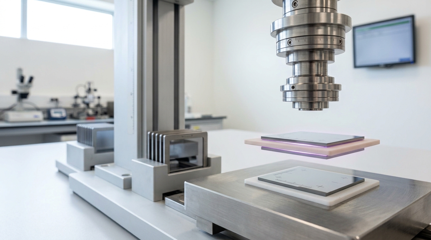
“Hybrid” bonding gets its name because it forms two different kinds of joint in the same operation: a dielectric-to-dielectric bond across most of the die’s face, and a metal-to-metal bond at the small fraction of that face occupied by copper contact pads. Both have to succeed, and they succeed through different physics, on different timescales, applied in a specific sequence.
The dielectric bond is a room-temperature, no-pressure event, and it is the more surprising of the two. imec researchers Chew, De Vos and Beyne describe the mechanism plainly: once two wafers with sufficiently flat, sufficiently clean dielectric surfaces are brought into contact, “the polished wafer surfaces adherence results in a strong wafer-to-wafer attraction, resulting in a bonding wave” that runs outward from the point of first contact across the rest of the wafer pair [4]. That wave is not a figure of speech; it is a physically observable front, driven by the same short-range surface forces that make two pieces of optically flat glass stick together, and it happens before any heat is applied. What makes the wave possible at all is a preceding activation step: SemiAnalysis’s process walkthrough describes treating the dielectric surfaces with nitrogen plasma before bonding, which raises their hydrophilicity enough that the two surfaces form an initial “weak dielectric-dielectric pre-bond at room temperature” through hydrogen bonding once they touch [9]. The surface has effectively been made sticky on purpose, and only for a limited time — plasma-activated bonds relax and airborne contaminants land on an exposed surface, so a wafer has to travel from the activation chamber to the bonder and make contact while the treatment is still live.
The mechanical tolerance behind all of this is severe. The same walkthrough states that dielectric roughness has to be held within half a nanometre, and copper pad roughness within one nanometre, across the entire bonding surface [9] — a tolerance that puts the whole burden on chemical-mechanical polishing rather than on ordinary machining. Copper pads are also deliberately recessed a few nanometres below the surrounding dielectric before bonding, so the dielectric contact happens first and the metal pads only meet once the wafers have been drawn fully together; at very fine pitch, however, the opposite geometry can be preferable. Sony’s own presentation at the IEEE Electronic Components and Technology Conference, as reported by SemiAnalysis, found that once pitch is scaled down to about one micrometre, the pads are better off protruding slightly rather than recessed [9] — a reminder that the correct pad geometry is not a fixed rule but a function of pitch.
The metal bond forms second, and it needs heat. imec reports that, using a silicon carbonitride dielectric, “the high bond strength can be obtained after post-bonding anneal at only 250°C and does not degrade at higher temperatures” [4], and a peer-reviewed Scientific Reports study gives a physical account of what is actually happening at the copper interface during that anneal. Jeong and colleagues bonded copper surfaces through various thin metal passivation layers — platinum, titanium, tantalum and chromium — and tracked how much copper diffused across the bonded interface. The result broke with the field’s usual assumptions: diffusion did not track the passivation layers’ surface roughness or grain size, but tracked their crystallinity instead, with copper diffusion measured by X-ray photoelectron spectroscopy at 200°C reaching 43.9% under a platinum layer against 0.2% under chromium, and platinum’s crystallinity measured at thirteen to twenty-three times higher than chromium’s along different crystal orientations [5]. Bonding through platinum succeeded at 260 to 280°C. The practical upshot is that copper-to-copper bonding is not simply “heat it until it sticks” — the specific metallurgy of the interface, not only its cleanliness, decides how readily atoms cross it and lock the two pads together as one continuous piece of metal rather than two pieces merely touching.
Wafer flatness across the whole 300-millimetre disc, not just at one bond pad, is what turns this from a laboratory result into a manufacturable process. imec and EV Group’s most recent public demonstration, reported in May 2026, pushed the interconnect pad pitch to 200 nanometres while holding “a Cu pad-to-pad post-bond overlay vector below 40 nanometres… for 100% of the dies over the full 300mm wafer,” which the two organisations describe as a world first [3]. Reaching it required an additional chemical-mechanical polishing pass immediately before bonding to flatten the dielectric and control the copper pads’ recess to within a few nanometres, together with a revised pad layout and lithography corrections applied before bonding to compensate for distortions introduced earlier in the flow [3]. None of that changes the underlying physics described above; it is what has to be added, layer by layer, to make wafer-scale uniformity keep pace with a shrinking pitch.

Cutting a hole through a wafer and not leaving it rough
A through-silicon via starts as a hole, and the hole is cut by deep reactive-ion etching using what is universally called, after the company that patented it, the Bosch process: the etch alternates rapidly between a fluorine-based etch step, typically using sulfur hexafluoride, and a fluorocarbon passivation step that protects the sidewalls just cut so the next etch pulse digs straight down rather than sideways. It is an efficient way to cut a deep, narrow, roughly vertical hole in single-crystal silicon, and it has one well-known side effect: each etch-and-passivate cycle leaves a small horizontal step on the sidewall, so a Bosch-etched via wall is not smooth but finely ridged — an effect universally called scalloping.
Scalloping is not cosmetic. The ridges concentrate mechanical stress, and a rough sidewall is a poor surface to plate copper onto evenly, which is exactly the next step a TSV has to survive. Frasca and colleagues at EPFL, publishing in Scientific Reports, addressed the problem with a second etch step applied after the Bosch process rather than a change to the Bosch process itself: a wet potassium hydroxide etch, applied to silicon wafers cut along the <110> crystal orientation and with the via pattern’s edges deliberately aligned to that crystal’s <111> planes, so that the anisotropic KOH etch removes only the protruding scallops and taper rather than attacking the via more broadly [6]. Concentrated to 40% and heated to 60°C for 45 to 60 minutes, the step — which the authors name for Michelangelo’s account of removing the “superfluous material” already implicit in a block of marble — brought a via etched to a record 28:1 aspect ratio down to what the authors describe as atomic-level sidewall smoothness, demonstrated on vias with a nominal minor diameter of one micrometre etched 40 micrometres deep [6]. The etch step and the smoothing step are doing genuinely different jobs: one removes bulk silicon fast along a rough vertical path, the other removes a small, geometrically specific amount of material to make that path’s walls trustworthy for what comes next.
Filling a hole from the bottom without leaving a seam
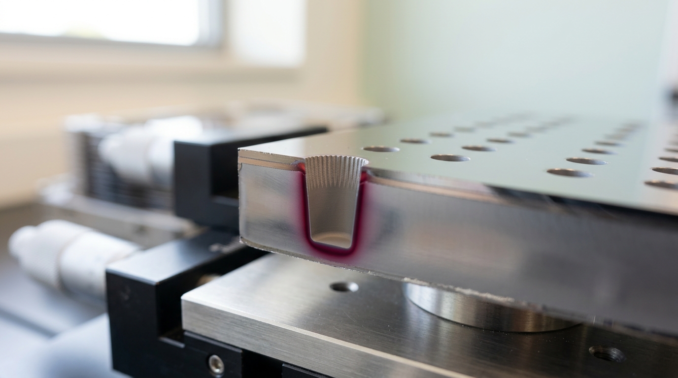
Once a via is etched and smoothed, it still has to become an electrical conductor, and the method almost universally used is copper electrodeposition — plating copper out of solution onto a seed layer that lines the via’s walls. The obvious way to do this, plating uniformly from every exposed surface at once, is also the wrong way: a via that plates evenly from its sidewalls and its bottom simultaneously closes near the top before the bottom has filled, sealing a void inside a structure that is supposed to be solid metal.
The standard fix is a plating bath engineered to plate from the bottom up instead, and the chemistry that does it is a competition between additives rather than a single ingredient. A copper sulfate and sulfuric acid bath carrying chloride ions is dosed with two organic additives that behave oppositely: a suppressor that adsorbs preferentially onto the via’s surfaces and slows plating, and a leveler that competes for the same surface with different kinetics. Tomie and colleagues, publishing in the Journal of The Electrochemical Society, used a microfluidic device to watch the two additives compete for the plating surface directly rather than inferring it from the plated result, and found that when both are present together, “the suppressor initially covered most of plating surface, but the leveler gradually replaced the suppressor, and the plating surface was finally dominated by the leveler” [7]. That displacement is the mechanism, not an incidental detail: a suppressor alone is not sufficient to force bottom-up fill, but the leveler’s stronger suppression and faster deactivation at the growing bottom surface are what actually drive copper to deposit preferentially at the via’s floor as it climbs, while the more slowly deactivating suppressor continues to hold back unwanted growth elsewhere on the surface [7]. The practical consequence is that TSV fill quality is set as much by bath chemistry and additive concentration as by the plating tool’s current and voltage — get the additive balance wrong and a via voids invisibly, closed at the top with nothing solid inside.

The interposer’s other job: making a trace disappear into the plane
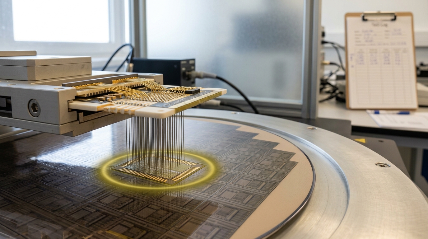
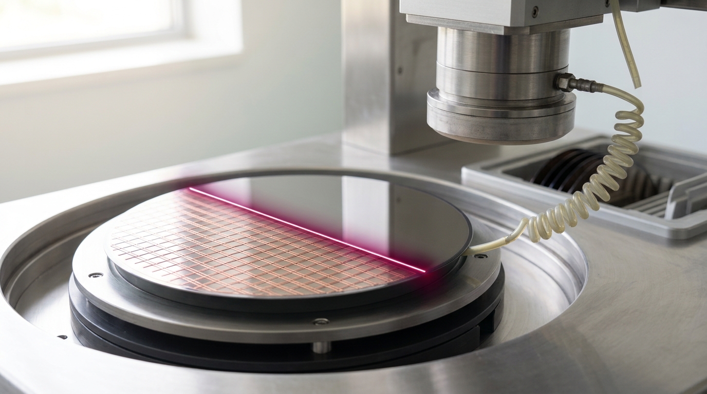
A through-silicon via only gets a signal a vertical connection. Most of a chiplet’s signals also have to move sideways — from a bond pad at one location on a die to a via, or an interposer edge, somewhere else — and that lateral routing is the job of a redistribution layer built directly on the interposer or on the die’s own back end. The way that layer is built is the same copper damascene process used throughout modern back-end-of-line fabrication, adapted to packaging scale: as Fadi Coder describes it in a 2025 IMAPS 3D InCites piece, “dual damascene etches precise cavities into the dielectric, then fills them with copper via electroplating,” after which chemical-mechanical polishing removes the excess “to produce a flat, inlaid surface, essential for multilayer stacking” [11]. That last clause is the connective tissue to the two previous sections: the same planarization discipline hybrid bonding needs at the die surface is needed again one layer down, every time another redistribution layer is added, and Coder makes the link explicit — “CMP’s excellent surface planarity supports direct layer-to-layer bonding” [11]. Recent seedless copper-plating chemistries, which eliminate the physical-vapour-deposited seed layer a conventional damascene flow requires, are reported to achieve void-free fill in features with aspect ratios from 2:1 to 5:1 while holding sub-2-micrometre line and space geometry [11] — fine enough to fan out a modern chiplet’s bond-pad pitch without a second, coarser routing layer standing between it and the package.
Making the layer flat and fine is a fabrication problem; what that layer then does to a signal is a separate, electrical one, and a through-silicon via is a genuinely awkward electrical object because it is not just a wire — it is a metal core wrapped in a thin insulating liner, sitting inside bulk silicon that is a fairly poor but not negligible conductor in its own right. Treated as a coaxial structure — copper core, oxide liner, conductive silicon beyond it — the liner behaves as a capacitor per unit length,
with
Density itself is worth being precise about, because pitch and area density do not scale the same way. If interconnects sit on a roughly square grid of pitch
not as
A physical bond needs a protocol before it is a link
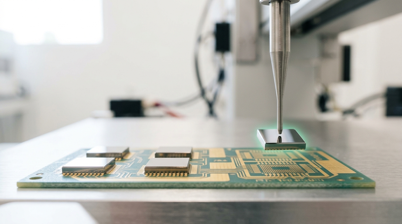
Everything above gets two pieces of silicon into electrical contact. None of it, by itself, gets one piece of silicon to understand what the other one is saying. That is the job of the Universal Chiplet Interconnect Express standard, an open specification maintained by a multi-company consortium specifically so a chiplet from one source and an interposer or base die from another can be connected without either side needing bespoke, proprietary signalling logic.
UCIe’s own specification describes itself as covering three things: “the die-to-die I/O physical layer, Die-to-Die protocols, and software stack” [1], which in practice separates into three layers doing distinct jobs. The physical layer is the electrical one — drivers, receivers, clocking and the link-training sequence that gets two chiplets’ interfaces synchronised in the first place — and Synopsys’s account of it, describing an implementation built to the standard, notes that the UCIe 2.0 specification defines data rates “of up to 32Gbps per pin” at this layer, with individual vendor implementations sometimes exceeding it while remaining compliant [10]. Above that sits a die-to-die adapter layer, responsible for “link management functionality as well as protocol arbitration and negotiation,” with an optional layer of cyclic-redundancy-check-based error detection and retry sitting at this level to catch the occasional bit flip a physical link this fast will produce [10]. Above that again sits the protocol layer proper, which “defines the rules and conventions for data exchange, including command sets and response formats” [10] — and rather than inventing a new transaction language from nothing, UCIe deliberately reuses two existing ones: the specification states it “leverages the well-established PCI Express (PCIe) and Compute Express Link (CXL) industry standards” [1], so a chiplet link can carry the same load and store, cache-coherent or streaming semantics software already expects from an on-board PCIe or CXL connection, just carried across a package seam instead of a circuit board. The newest revision adds a third option to that list — a Raw Mode built for “continuous transmission protocols… enabling uninterrupted data flow… for new applications such as connectivity between SoC and DSP chiplets” [1], a tacit admission that not every chiplet-to-chiplet relationship looks like a memory or input-output transaction, and some are closer to a dedicated, always-on data pipe.
The physical layer’s electrical target changes sharply depending on which of the previous sections’ technologies is actually carrying the signal. UCIe’s own specification states that its UCIe-3D variant “is optimized for hybrid bonding with a bump pitch functional for bump pitches as big as 10-25 microns to as small as 1 micron or less” [1] — the same hybrid-bonded, direct copper-to-copper connection described earlier in this article, at the same pitch range imec’s public results are pushing toward. That single sentence is where this article’s separate threads actually meet: the standard’s physical layer is defined to sit directly on top of a hybrid-bonded interface once the pitch gets fine enough, rather than treating hybrid bonding as an alternative to UCIe.
The specification has also moved fast since its first release, and each revision has targeted a specific limitation rather than simply promising more bandwidth. UCIe 1.1 added runtime health monitoring and repair aimed at automotive and high-reliability applications, along with new bump maps intended to lower packaging cost. UCIe 2.0 added a management fabric — the UCIe DFx Architecture — inside each chiplet for test, telemetry and debug, alongside formal 3D-packaging support [1]. UCIe 3.0, announced in August 2025, doubled the maximum data rate to 48 and 64 gigatransfers per second from 2.0’s 32, extended the sideband channel’s reach to 100 millimetres for more flexible system-in-package layouts, added runtime transmitter-side recalibration, and added a lower-power idle state intended to support more aggressive power gating between bursts of traffic, while stating full backward compatibility with earlier implementations [2]. None of that revision history changes what the protocol layer fundamentally does; it is the specification catching up to what hybrid bonding, TSVs and fine-pitch interposers made physically possible underneath it.
Reading a packaging spec after knowing what is under it
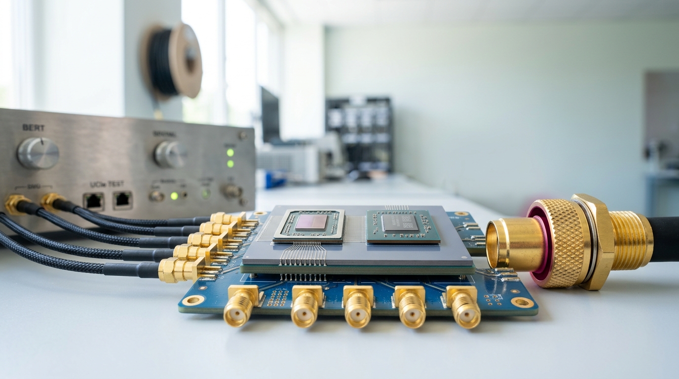
Put the four mechanisms back together and a packaging claim stops reading like a marketing sentence and starts reading like a list of things that had to go right, in a specific order. “Hybrid-bonded chiplets at fine pitch” means a dielectric surface was plasma-activated, pressed flat against another to within a fraction of a nanometre, and annealed until copper atoms actually crossed the boundary between the two pads — and that the passivation metallurgy and anneal temperature chosen were compatible with whatever was already built underneath that layer. “A silicon interposer with a dense through-silicon-via field” means each via survived a Bosch etch, a scalloping-removal step and a bottom-up copper fill without a hidden void — and that its electrical behaviour, capacitive at low frequency and increasingly resistive and inductive as clock rates climb, was accounted for in how signals were routed across it rather than assumed away. “UCIe-compliant at one-micrometre pitch” means the physical layer sitting on top of all of that has a training sequence able to lock onto a link this short and this dense, running a protocol stack that, underneath the acronym, is still mostly PCIe or CXL wearing a different physical layer and a shorter commute.
None of this is exotic science; every mechanism above has been published, and several of the specific figures cited — imec’s 200-nanometre pitch, the Michelangelo step’s 28:1 aspect ratio, UCIe 3.0’s 64-gigatransfer data rate — are recent enough that the field is still actively moving on them. What has changed is where the argument for a package’s performance actually lives. It used to be settled almost entirely inside one piece of silicon, in the transistors. Increasingly it is settled in a plasma chamber, a Bosch etcher, a copper-plating bath, a chemical-mechanical polisher, and a specification committee — five places that do not appear on the die photo at all, and that this article has tried to make visible instead.