Someone else’s silicon, on your floorplan
Chip design teams have spent decades optimizing what happens inside one piece of silicon. Floorplanning a multi-die package asks a different question: not where does this block go inside my die, but where does this die — designed by a different team, on a different process, sometimes at a different company entirely — go relative to everyone else’s, and what does that placement cost in wirelength, heat, and mechanical stress simultaneously. This is now the actual job for a growing share of chip design teams. A frontier accelerator or a modern server processor is rarely one piece of silicon anymore; it is several, floorplanned onto a shared interposer or substrate, connected by a standardized electrical interface, and co-designed thermally and mechanically as one assembly even though it was never designed as one piece.
The companion pieces in this series have already made the case for why this shift happened — the reticle limit on a single die, the yield-versus-area tradeoff, the packaging capacity constraint that now rivals wafer capacity as the thing that decides whether a product ships. This article does not repeat that case. It is written for the team that has already decided to build a multi-die package and now has to actually do it: floorplan the dies onto the carrier, hold UCIe’s electrical and protocol constraints without pretending the standard settles more than it does, keep every die in the stack within its thermal and mechanical budget at once, and get through the specific, repeated ways that “buy the chiplet and drop it in” integration goes wrong in practice.
None of what follows is hypothetical. Every design methodology, every constraint number, and every failure pattern below comes from a published specification, a peer-reviewed or preprint floorplanning paper, an EDA vendor’s own test methodology documentation, or a foundry’s own packaging design-flow announcement — attributed as such throughout, because the difference between “the standard requires this” and “a vendor is proposing this as a solution” matters for a team about to make a real, expensive commitment.
Floorplanning a multi-die package: wirelength is now the least binding constraint
On a single die, floorplanning is mostly a wirelength and congestion problem: place related blocks near each other, keep timing-critical paths short, route around macros. Extend the same problem across a package boundary and two things happen that don’t happen inside one die. First, the objects being placed are no longer freely resizable blocks of RTL — they are fixed, already-fabricated pieces of silicon, or at the floorplanning stage faithful physical proxies of pieces that will be fabricated, each with its own footprint, thickness, and thermal design power, arriving from a process and a design team the integrator does not fully control. Second, minimizing wirelength between them is no longer the objective by itself, because packing dies tightly to shorten the wires between them is exactly the choice that concentrates heat and mechanical stress into the same small footprint.
Ma and colleagues’ TAP-2.5D methodology made this tradeoff explicit in one of the first open floorplanning tools built specifically for 2.5D systems: rather than minimizing wirelength as the sole objective, TAP-2.5D deliberately inserts spacing between chiplets to jointly reduce peak temperature and total wirelength together, and reports that doing so measurably increases the system’s usable thermal design power envelope [5]. That is a genuinely counterintuitive instruction for anyone trained on single-die floorplanning: part of the tool’s job is to keep dies apart, not only to keep them close.
More recent work adds a second axis TAP-2.5D did not model. Parekh and colleagues’ STAMP-2.5D methodology couples thermal and structural-mechanical optimization in the same automated floorplanner, on the observation that tightly packed placements which look thermally fine can still concentrate coefficient-of-thermal-expansion mismatch into localized mechanical stress that a temperature-only objective never sees; their finite-element-based floorplanner reports an 11 percent reduction in peak mechanical stress against a temperature-only baseline, while holding the resulting temperature increase to a reported 0.5 percent and simultaneously cutting total wirelength by roughly 11 percent as well [4]. The practical lesson generalizes past the specific numbers: a floorplan that only tracks wirelength and temperature can still be a mechanically bad floorplan, because the coefficient-of-thermal-expansion mismatch between a silicon logic die and its neighboring memory stack, its interposer, and its organic substrate does not show up in either of those two metrics on its own.
A floorplanning objective built to hold all three properties at once is naturally written as a weighted combination rather than a single term:
where
Roman-Vicharra and colleagues add a third complication that neither TAP-2.5D nor STAMP-2.5D directly addresses: in a genuinely heterogeneous package, the dies being floorplanned were not all built on the same process node, so their footprint, and therefore the floorplan itself, is coupled to a technology-assignment decision that is normally made earlier and separately. Their framing is explicit — “different dies may employ distinct technologies, making floorplanning across multiple dies inherently coupled with technology assignment” — and their tool treats node selection as a variable inside the floorplanning loop rather than a fixed input to it, using fast machine-learned power-performance-area estimation to keep the resulting search tractable [6]. In practice, this is the mundane but entirely real problem of a die sourced from a foundry partner arriving a different thickness than the logic die it sits beside, forcing a substrate or interposer redesign that a same-node, in-house floorplan would never have encountered.

What UCIe actually settles, and what it leaves for you to solve
It is tempting to read “the die-to-die interface is now standardized” as “the interoperability problem is solved,” and the temptation is worth resisting carefully, because the standard is genuinely narrower than that reading implies.
UCIe’s own specification history shows what has actually been standardized, version by version: version 1.0 defined the die-to-die physical layer, protocol stack, software model, and a compliance test programme; 1.1 stayed backward compatible while adding runtime health monitoring and lower-cost bump maps; 2.0 extended the standard to 3D packaging, specifying bump pitches from roughly 10 to 25 micrometres down to 1 micrometre or smaller; and 3.0 doubled the top data rate to 48 and 64 gigatransfers per second for both standard-package and advanced-package links while extending sideband reach to 100 millimetres, remaining backward compatible throughout [1]. That is the electrical and protocol layer, precisely specified and versioned like any serious interconnect standard.
The physical numbers matter for floorplanning specifically, because they set a hard geometric constraint on how close two dies must sit to use each package option. Mota’s account of the standard, published as UCIe reached its first release, gives the two reference configurations concretely: an advanced-package link runs a 45-micrometre bump pitch with a channel reach beyond 2 millimetres, 64 transmit and receive pins per module, and 16 gigabits per second per pin for roughly 4 terabits per second of bidirectional bandwidth per module; a standard-package link runs a coarser 110-micrometre bump pitch with reach beyond 10 millimetres, 16 pins per module, and roughly 1 terabit per second bidirectional at the same per-pin rate [2]. Choosing advanced package over standard package is not a software configuration choice — it is a floorplanning decision made before the interposer is designed, because it fixes how far apart the two dies on either end of the link are allowed to sit.
Below the physical layer, the die-to-die adapter is where UCIe does the negotiation work that lets genuinely different vendor implementations talk to each other at all. Koziuk’s detailed account of the adapter layer describes a staged link initialization in which the sideband channel first advertises each side’s supported flit formats — a 64-byte raw format for streaming protocols, a 68-byte format capped at 32 gigatransfers per second, and 256-byte formats built on the PCIe and CXL specifications — along with retry support and per-protocol bandwidth limits, before the two sides settle on a shared configuration and begin transferring flits [3]. The adapter also supports sharing one physical link across more than one protocol stack: in a regular mode, two identical protocol implementations can each take half the bandwidth, while an enhanced mode lets genuinely different protocols multiplex the full link, interleaving no-op flits so that consecutive flits from the same stack never collide [3]. This is real, working interoperability machinery, not a marketing simplification of one.
What none of that negotiation touches is the thing a floorplanner actually has to decide first: whether two specific chiplets’ physical bump maps are compatible at all. UCIe standardizes the pitch options and the protocol that runs over them; it does not standardize where on a given die’s edge the UCIe bumps sit, in what orientation, or how they interleave with that die’s power and ground bumps — those remain implementation choices each chiplet’s own designer made independently, for their own reasons, before UCIe compliance was ever tested. Two UCIe 2.0-compliant advanced-package chiplets from two different vendors can both pass the electrical compliance programme individually and still require a redistribution layer, a bridge, or a custom interposer route to actually connect their bump fields to each other, because “compliant” describes the electrical and protocol behaviour at the pins, not the geometric arrangement of the pins themselves. That gap is exactly where a floorplanning team’s real work sits, underneath a standard that has already solved a real and different problem.
Thermal co-design across a heterogeneous stack
A monolithic die has one thermal problem: get the heat generated across its area to the heat sink through one stack of known materials. A heterogeneous multi-die package has several thermal problems stacked and interleaved, because logic, memory, and any tiers bonded above them generate heat at different rates, sit at different distances from the heat sink, and are made of materials with different thermal conductivity — and a compact thermal model built for a single die does not automatically generalize to that arrangement.
Zhu and colleagues’ 3D-ICE 4.0 framework was built specifically because existing compact thermal modeling struggled to scale with exactly this complexity and heterogeneity; their tool preserves material properties from the actual industrial design rather than approximating them, partitions the vertical stack adaptively rather than uniformly, and generates a temperature-aware simulation grid, reporting a speed-up of roughly 3.6 to 6.5 times alongside more than a 23 percent reduction in grid complexity relative to earlier approaches, specifically so that both lateral heat spreading within a tier and vertical heat flow between tiers can be captured together at a computational cost a design team can actually afford to run repeatedly during floorplanning [8]. The existence of a tool built around that specific gap is itself informative: as of the tool’s own framing, thermal modeling that treats a heterogeneous stack as a scaled-up version of a single-die problem was not good enough, and the field needed a purpose-built replacement.
The design lesson that follows is the same one TAP-2.5D encoded directly into its floorplanner: the placement that minimizes wirelength is frequently not the placement that minimizes peak temperature, because packing dies edge-to-edge concentrates every die’s heat into the smallest possible footprint on the shared carrier, and a tight floorplan does not get to choose which specific die ends up sitting in the resulting hotspot [5]. Practically, this means thermal co-design cannot be a verification step run once a floorplan is otherwise finished — it has to sit inside the same optimization loop as the placement decision, run early enough that the answer can still change where a die goes rather than only how much heat sink gets bolted on top of where it already is. STAMP-2.5D’s own reported results make the size of the effect concrete: holding thermal performance within half a percent of a temperature-only optimum while cutting mechanical stress by roughly 11 percent shows that a floorplanner with a richer objective does not have to trade thermal performance away to gain the other properties it is now also tracking — it can hold thermal roughly fixed while genuinely improving what a temperature-only tool was blind to [4].
The mechanical half of the same problem: warpage, CTE, and where it bites
Heat and mechanical stress are coupled in a heterogeneous package for a specific physical reason: every material in the stack expands at its own rate as temperature changes, and a joint between two materials with different coefficients of thermal expansion is where that mismatch has to be absorbed, cycle after cycle, as the assembly heats up under load and cools when it idles. STAMP-2.5D’s authors name this directly as their motivating problem — conventional wirelength-first placement, by packing chiplets tightly, intensifies coefficient-of-thermal-expansion mismatches, compromising long-term reliability even where the thermal picture alone looks acceptable [4]. A floorplan can pass a thermal check and still be a mechanically fragile one, because temperature and stress are correlated but not identical quantities, and historically only one of them was actually in the optimization loop.
This is also where the choice of package architecture, not only the placement within it, changes the mechanical exposure a floorplanning team is signing up for. A full silicon interposer spans the entire multi-die footprint and inherits the mechanical behaviour of a single large, stiff, brittle sheet of silicon bonded to a comparatively soft organic substrate underneath it — the larger that sheet, the more of the substrate’s own thermal expansion it has to resist rather than follow. A bridge-based approach embeds a small silicon structure only where two specific dies actually need a fast, fine-pitch connection, leaving the rest of the package on ordinary organic substrate; Intel’s own account of EMIB’s original motivation describes it as solving an interconnect-density problem — routing enough signals in and out of a chip at a fine enough pitch — while explicitly allowing a design to mix and match technologies, including different process nodes or even different vendors, because the bridge, unlike a full interposer, only has to be exactly as large as the seam it crosses [10]. That is a mechanical decision wearing an electrical-interconnect description: a smaller embedded structure has less area over which to accumulate CTE-driven stress against the substrate beneath it, which is a genuine reason a floorplanning team might choose a bridge architecture even when a full interposer would technically support more aggregate bandwidth.
Foundries have started building mechanical and thermal checks directly into the earliest stage of the design flow rather than leaving them for post-floorplan verification. TSMC’s own description of its 3Dblox 2.0 standard frames this as the point of the release: it lets a design team combine power-domain specifications with the physical 3D construction of the package and simulate power and thermal behaviour for the whole assembly at the feasibility stage, before committing to a specific floorplan, and pairs that capability with a dedicated 3Dblox standards committee drawing on multiple EDA vendors specifically to keep power and thermal feasibility checking available across tool vendors rather than locked to one company’s own flow [9]. Read against the floorplanning papers above, that is the foundry side of exactly the same lesson: mechanical and thermal co-design has to happen at the same stage as placement, because by the time a floorplan is otherwise finished, the cheapest fixes for a warpage problem are already gone.
Where third-party integration actually breaks
The pitfalls that recur when a design team integrates a chiplet it did not design are not, in practice, primarily electrical. UCIe’s compliance programme is built to catch electrical and protocol mismatches before a package is ever assembled. What it does not directly catch is a longer list of test, verification, and trust problems that only become visible once a specific vendor’s specific die is sitting in a specific package.
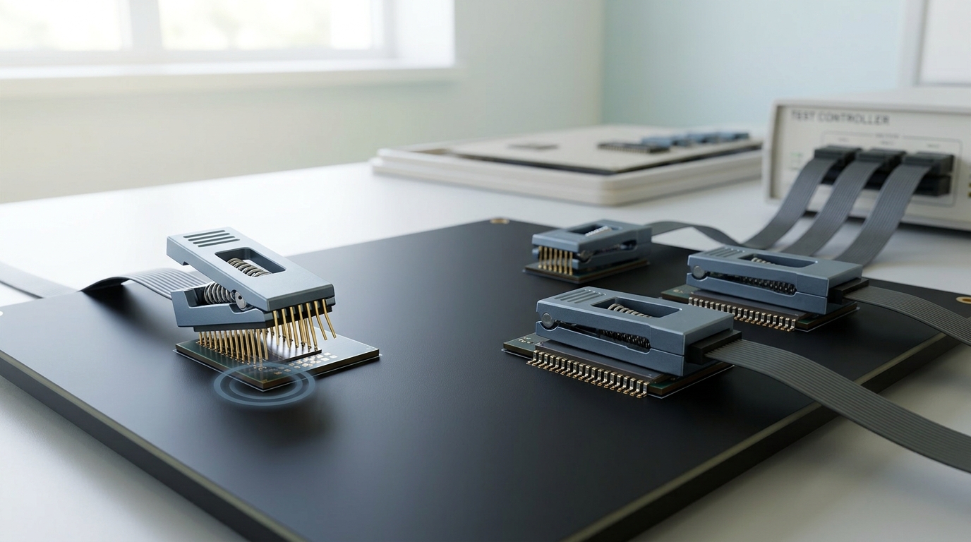
Known-good-die testing is the first and most consequential of these, precisely because a multi-die package cannot recover from an undetected bad die the way a repair mechanism inside one large die sometimes can — once a chiplet is bonded into an assembly, removing it destroys the assembly around it. Eximietas’ account of the practical challenges lists eight specific, concrete failure points design teams run into: verifying each chiplet’s function across its full operating corner before assembly rather than after; a dedicated pad-loopback test design on every die-to-die interface, so that the interface itself, not just the logic behind it, is proven at full speed; the need to retarget test patterns from a single-die test flow to a multi-vendor, multi-die assembly without losing coverage; built-in redundancy so a partially defective die can still contribute a working subset of its function; structural test architecture that does not blow the power budget of the assembled package while it runs; a recovery path for defects discovered late, after significant assembly value has already been committed; a unique device identifier scheme reaching down to the individual die level for field traceability and warranty investigation; and authenticated access control on each chiplet’s own test infrastructure, so that one vendor’s chiplet cannot become an unauthorized access point into the rest of the package [11]. None of these is exotic; all eight are routine, named engineering requirements, and all eight get harder specifically because the dies involved were not all designed, tested, or documented by the same team.
McMillan’s account of the same problem from the design-for-test tooling side names the structural cause underneath several of those eight points: dies buried inside a stacked or embedded configuration frequently have no direct connection to the package’s own external pins, so getting a test pattern to them and a result back out requires a deliberate routing strategy rather than the direct pin access a single packaged die takes for granted, and the standard answer draws on IEEE 1149.1 boundary scan, IEEE 1687 for embedded instrument access, and IEEE 1838 specifically for testing 3D-stacked dies before, during, and after bonding [7]. A chiplet integration flow that treats test access as something to solve after the floorplan is fixed will discover, specifically at the die that ended up buried furthest from the package’s own pins, that there was no route left to give it.
The subtler pitfall sits one layer above all of this, in what an integrator has to take on trust rather than verify directly. A third-party chiplet arrives with a vendor-supplied model — electrical, thermal, and behavioural — standing in for a design the integrator did not do and, for intellectual-property or competitive reasons, frequently cannot fully inspect. Every piece of co-design described in this article, from STAMP-2.5D’s finite-element stress model to 3D-ICE 4.0’s thermal grid, is only as accurate as the material properties, power maps, and boundary conditions fed into it, and for a bought-in die those inputs are exactly the fields the integrating team is least able to independently confirm. This is not a solved problem with a standard behind it the way the electrical interface is; it is a trust and verification gap that UCIe compliance testing, known-good-die screening, and thermal-mechanical co-design each narrow from a different angle, without any single one of them closing it outright.
A practitioner’s sequence, in the order the decisions actually have to be made
Put the pieces above in the order a real design team actually has to resolve them, rather than the order a textbook would present them, and the sequence looks like this.
Decide package architecture before floorplanning starts, not after. Whether the design needs a full interposer, a bridge, or a fan-out redistribution layer is a mechanical and cost decision as much as a bandwidth one, and it bounds every placement choice that follows — a bridge architecture, for instance, only makes sense once the pairs of dies needing a fast connection are already roughly known.
Fix the UCIe package type — standard or advanced — for each link before the interposer geometry is drawn, because the bump pitch and channel reach that choice implies is a hard geometric constraint on how close those two dies can sit, not a parameter to be tuned later [2].
Run thermal and mechanical co-design inside the placement loop, not after it, using a tool built for heterogeneous stacks rather than a single-die thermal model extended by hand [8, 4]. A floorplan that has already been fixed for other reasons before thermal and stress checking begins has already thrown away its cheapest fixes.
Resolve bump-map compatibility explicitly for every third-party chiplet pairing, treating UCIe compliance as necessary but not sufficient — confirm the physical bump arrangement, not only the electrical behaviour at the pins, before committing to a floorplan that assumes two dies can simply be wired together [1].
Build the known-good-die and test-access strategy at the same stage as the floorplan, specifically for whichever die ends up buried furthest from the package’s own pins, using the IEEE 1149.1, 1687, and 1838 access mechanisms designed for exactly this problem [7], and plan test-pattern retargeting and device-level traceability before assembly begins rather than after a defect is found [11].
Treat every third-party model — electrical, thermal, behavioural — as a claim to be checked wherever checking is possible, not a settled input, because it is the one part of this sequence with no standard, no compliance programme, and no automated tool behind it.
None of these six steps is optional in the sense that skipping it merely adds risk that shows up later; each is a decision that becomes progressively more expensive to revisit the further the design proceeds past it, which is the entire reason the order matters as much as the content.
What to take away
Floorplanning a multi-die package is not single-die floorplanning at a larger scale; it is a different problem, because the objects being placed are already fixed, already fabricated, and frequently designed by someone else, and because minimizing wirelength between them is no longer the objective on its own. UCIe genuinely solves the electrical and protocol layer of getting one vendor’s chiplet to talk to another’s — the specification, the compliance programme, and the adapter’s negotiation machinery are real, versioned, and increasingly capable. It does not solve bump-map compatibility, thermal-mechanical co-design, known-good-die screening, test access into a buried die, or trust in a third-party model, and treating the standard as though it had already solved those is the single most common way a chiplet integration schedule slips. Every one of those remaining problems already has a methodology, a tool, or a foundry-level design flow built for it, cited throughout this piece rather than invented for it. The discipline this practice actually requires is running them early enough, and in the right order, that their answers can still change where a die ends up, rather than only how much correction gets bolted on after it is already there.