Thirty-Two Terabytes Is a Real Number; It Is Not the Number You Think It Is
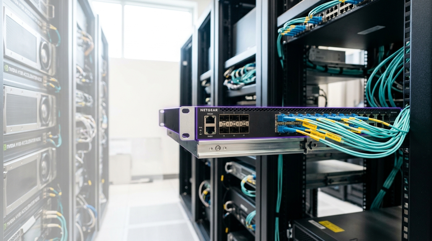
Sixteen modules, one rack appliance, thirty-two terabytes of memory that every processor in the system can address as if it sat next to the die. That is the headline Celestial AI put on its Photonic Fabric Module, and it is the kind of number a reader is invited to round up in their head to “thirty-two terabytes of fast memory” — HBM-class memory, the kind that currently caps out in the low hundreds of gigabytes on a single accelerator (141 gigabytes on NVIDIA’s own H200 [5]) and forces every large-model deployment to shard a model across chips it would rather keep on one. The vendor’s own component count does not support that reading. Work through what is actually inside one module, multiply it by sixteen, and there is no way to reach thirty-two terabytes without most of that pool being ordinary DDR5 — the memory that has sat behind a comparatively slow, high-latency bus for two decades, not the memory that sits on an interposer next to a GPU die. That arithmetic does not undercut the product. It relocates the claim under test. The interesting question was never whether this fabric makes DDR5 as fast as HBM3e; nothing does that, and nobody building it claims otherwise. The interesting question is whether making tens of terabytes of ordinary memory optically addressable, as one flat pool, at low enough latency to matter, is a genuine architectural shift in what “local” means to a die — or a bandwidth increase wearing a bigger word.
Celestial AI is the company that built this technology; it is not, any longer, the company that owns it. The firm’s own corporate domain now forwards directly to Marvell’s [7], the custom-silicon house that absorbed Celestial AI’s photonic-interconnect team and technology into a pipeline it describes as 18 XPU and XPU-attach sockets, an in-house 2.5D advanced-packaging platform, and a new die-to-die interface running 64 gigabits per second per wire in 2-nanometer silicon [8]. None of what follows is about that deal’s price or its logic as an acquisition — that is a separate story, told elsewhere. What matters here is narrower: the Photonic Fabric Module’s own disclosed specifications, whoever now owns them, and what they do and do not prove about turning off-package memory into an extension of the die.
One Module, Four Tapeouts, and a Switch That Doesn’t Sit at the Edge
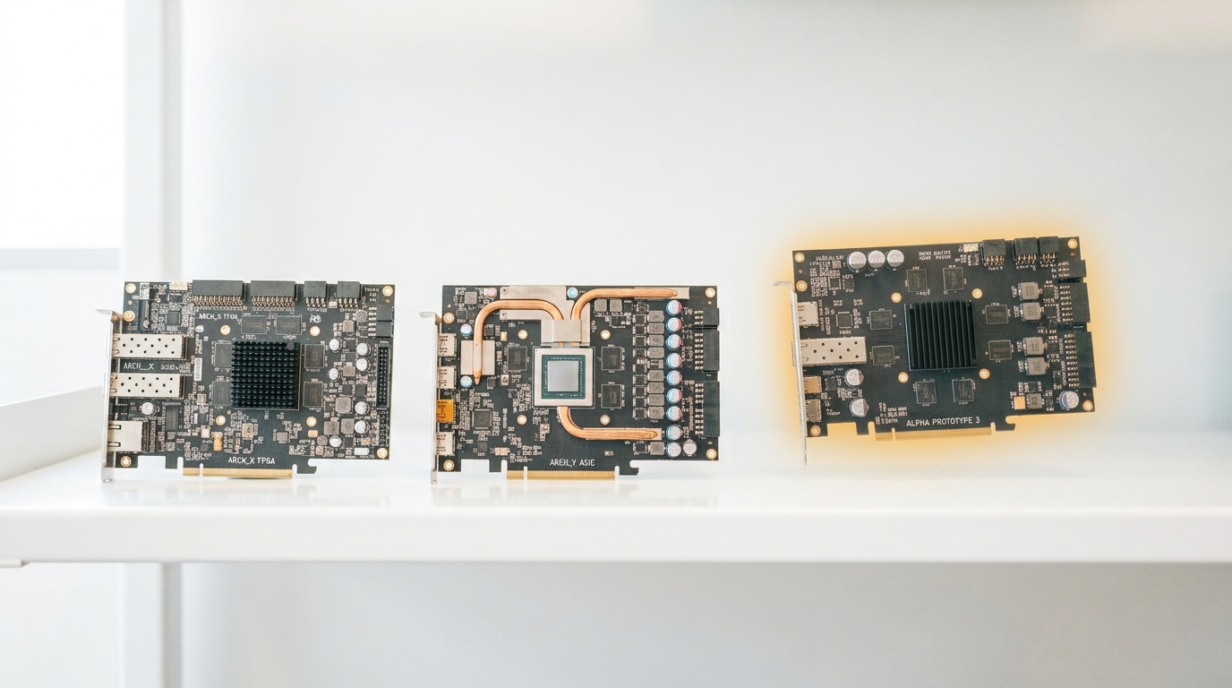
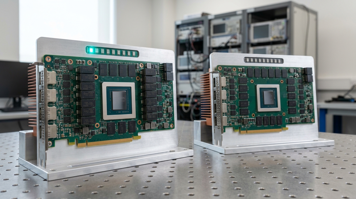
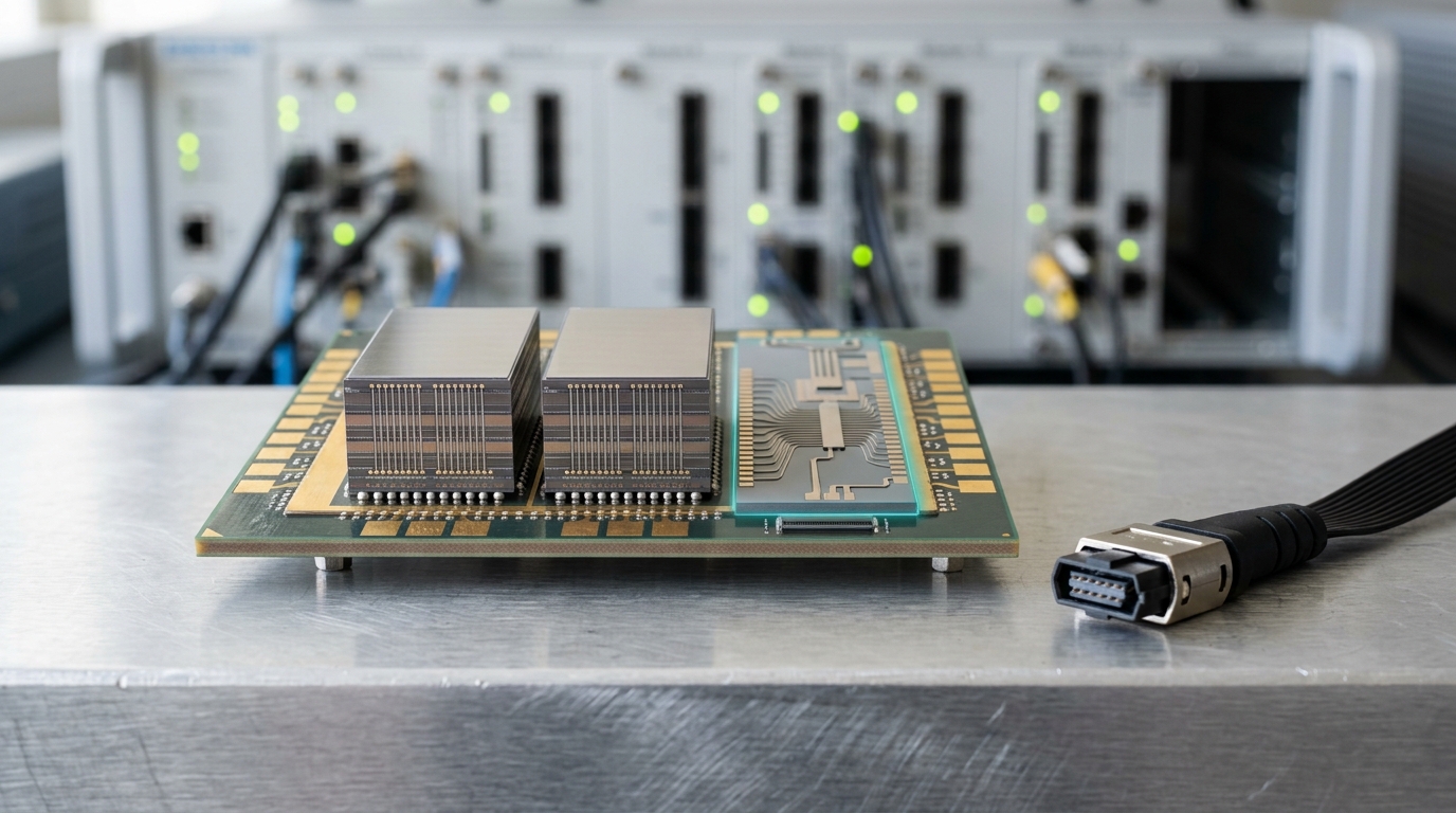
Strip the module down to what its own spec sheet states. A single Photonic Fabric Module pairs an eight-terabit-per-second switch, two HBM3e memory controllers, and four DDR5 controllers on one TSMC 5-nanometer ASIC, built into a 2.5D package alongside two physical HBM3e stacks, and delivers 7.2 terabits per second of optical connectivity out of the module [1]. A second product variant in the same family, the PF-Chiplet, pushes that figure to 14.4 terabits per second of optical connectivity per chiplet; a third, the PF-NIC, holds the same 7.2 terabits per second as the base module but swaps its host-facing interface for PCIe 6 and CXL 3.1 support, so a rack-scale host can reach the pooled memory as a standard CXL device rather than through a proprietary switch-fabric link [1]. Wire sixteen of the base modules together and the company’s own materials state the result plainly: a rack-mountable Photonic Fabric Appliance offering a unified memory address space of up to thirty-two terabytes [1].
The mechanical trick underneath those numbers is not, primarily, a bandwidth trick — it is a placement trick. At Hot Chips 2025, Celestial AI’s own presentation described the interconnect as built from a silicon-photonics layer using electro-absorption modulators rather than the ring modulators common elsewhere in the industry, integrated through what the company calls an Optical Multichip Interconnect Bridge, in a TSMC CoWoS-L package, with a sixteen-port switch and four completed tapeouts behind it [2]. The detail that matters most for the “extension of the die” framing is the bridge itself: it lets optical input and output land anywhere across a chip’s surface, not only around its rectangular perimeter [2]. A conventional accelerator die is edge-limited by construction — every HBM stack, every high-speed SerDes lane, every interposer trace has to reach the die from outside its boundary, and a die’s edge is a fixed, comparatively short perimeter that does not grow as fast as the silicon area behind it does. NVIDIA’s own Blackwell architecture shows the same constraint from the compute side of the same problem: two reticle-limited dies, each already at the largest size a lithography system can expose in one shot, are stitched together with a ten-terabyte-per-second copper link rather than fused into one larger die, precisely because there was no more edge left to route through [6]. An optical bridge that can land a connection in the middle of a package, not only along its rim, is solving the same shortage of edge a different way — with light instead of a second reticle.
Read as a family rather than three unrelated products, the trade-off across PF-Chiplet, the base PFM, and PF-NIC is legible on its own terms. PF-Chiplet trades reach for raw rate, staying inside one package at double the per-link bandwidth of the module. The base PFM gives up some of that rate to reach an entire rack’s worth of modules through the appliance’s optical fabric. PF-NIC keeps the base module’s own 7.2 terabits per second rather than trading any of it away, and spends its design budget instead on swapping Celestial AI’s own switch-fabric link for PCIe 6 and CXL 3.1 — a standard interface a much larger population of hosts already knows how to use [1]. None of the three headline numbers is simply “better” than the others; 14.4 terabits per second per chiplet is not an improvement on 7.2 terabits per second per module unless the comparison specifies which reach each figure has to cover, and a flat “terabits per second” headline erases exactly that scoping by default.
The one number Celestial AI’s own technical disclosure did supply that speaks directly to what “local” means in practice is latency, not bandwidth: the PF-NIC variant reaches pooled memory across the fabric in under 250 nanoseconds [1]. That figure belongs specifically to the CXL-attached, rack-pooled access path, not to every access pattern the fabric supports, and it should not be read as a blanket number for the whole product family. But it is a real, disclosed figure, and it is the kind of number that a genuinely local resource is supposed to produce — closer to a same-package hop than to a network round trip.
The Math Only Closes If Most of the Pool Is the Slow Tier
Here is the arithmetic the spec sheet invites and never finishes itself. Sixteen modules, two HBM3e stacks apiece, is thirty-two physical HBM3e stacks across the whole appliance. Micron’s own HBM3E product line — used here only as one representative, publicly documented example of the memory class Celestial AI’s controllers are built to drive, not a claim about which vendor’s silicon sits in this specific module — ships an eight-high stack at 24 gigabytes of capacity today and describes a twelve-high, 36-gigabyte configuration as a further step in the same family [3]. Multiply either figure by thirty-two stacks: 768 gigabytes at the shipping capacity, 1.15 terabytes at the higher-layer configuration. Against a stated pool of 32 terabytes, that is a range of roughly 2.3 to 3.5 percent. The other 96 to 98 percent of the advertised address space cannot be HBM3e. It has to come from the four DDR5 controllers per module — sixty-four DDR5 channels across the whole appliance — and DDR5 is where the arithmetic gets genuinely interesting rather than merely deflating.
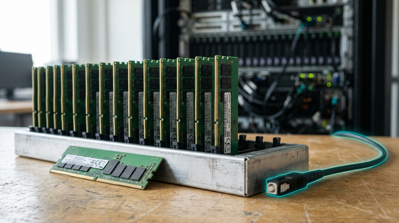
Sixty-four channels have to supply roughly 31 of the pool’s 32 terabytes, which works out to close to 480 gigabytes of DDR5 capacity behind every single channel. Micron’s current DDR5 RDIMM line ships at up to 128 gigabytes in volume today and is sampling a 256-gigabyte module as its next step [4]. Even at that still-sampling 256-gigabyte ceiling, one module per channel supplies barely half of what the arithmetic demands — the fabric’s spec sheet only closes if each of those DDR5 controllers is driving something closer to two of the industry’s largest currently-sampling modules, or an equivalent higher-rank configuration the public disclosure does not specify. That is not a contradiction in Celestial AI’s numbers; multi-DIMM-per-channel and multi-rank topologies are ordinary in server memory design, and a controller count on a spec sheet was never a promise of exactly one DIMM per controller. But it is a real gap in what has been publicly disclosed, and it means a reader cannot verify the 32-terabyte figure from the component list alone — only from a design detail the company has not put in writing anywhere this search could reach.
None of this weakens the underlying claim; if anything, it sharpens it into the shape the “extension of the die” framing actually needs. A pool that is almost entirely DDR5-class memory, made addressable as one flat space at rack scale, is not competing with HBM3e on speed — nothing built from DDR5 silicon plausibly could, and Celestial AI has never claimed otherwise. It is competing with the alternative of not having that memory reachable from the die at all except through a conventional, much slower, and much more topology-constrained network path. The real object under test, once the arithmetic is done, is exactly the object the dossier for this piece set out to measure: not “is the pool fast,” but “does optical reach change what a system can treat as local, and does that change survive being priced in energy rather than announced in a press release.”
A Locality Index Measures the Claim Precisely — When the Vendor Discloses What It Needs
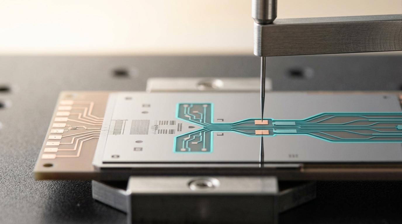
I define a compute-to-memory locality index,
Here
That is a clean, falsifiable test in principle. In practice, computing
The amortization term in that denominator matters more than it looks at first pass. A fixed integration cost — the extra laser sources, the photonic-PIC yield loss, the switch die itself — divided across a single module looks catastrophic; divided across sixteen thousand modules in a hyperscale fleet looks close to free. That is precisely why
The One Missing Number Is the Only One That Would Settle This
The copper side of the ratio fares only slightly better, and for an instructive reason: the closest available real-world figure is not a clean memory-subsystem number either. NVIDIA’s H200 accelerator ships 141 gigabytes of HBM3e and delivers 4.8 terabytes per second of memory bandwidth at a rated thermal design power of up to 700 watts in its SXM configuration [5]. Dividing one by the other gives a bandwidth-per-watt figure for the whole package — but the whole package’s power budget includes its compute cores, not only its memory interface, and there is no public disclosure that isolates how many of those 700 watts the HBM3e subsystem itself actually draws. Using the whole-package figure as
Put the two problems together and the honest conclusion is not “the locality index favors light” or “the locality index favors copper.” It is that the index, as formally defined, currently cannot be computed for this product at all — not approximately, not with an acknowledged error bar, but literally: one of its four required inputs has never been publicly disclosed by anyone in a position to measure it, and the other three are proxies with a known directional bias. That is a stronger and more useful finding than a fabricated point estimate would have been. It names, exactly, what would have to change for the debate to move: either Celestial AI’s technology under Marvell publishes a wall-plug power figure for the fabric — the switch ASIC, the optical links, the fixed per-module overhead — measured independently of the compute silicon it feeds, or a third party benchmarks a deployed Photonic Fabric Appliance’s power draw against its sustained random-access throughput directly, the way hyperscalers already do for GPU racks. Until one of those two things happens, “extension of the die” is a claim about locality and reach that the public record supports, sitting next to a claim about energy efficiency that it does not yet make possible to check.

| What the index needs | Disclosed for the optical case (PFM) | Disclosed for the copper baseline (H200-class) |
|---|---|---|
| Realized random-access bandwidth | Partial — aggregate peak figures only [1] | Yes — rated peak bandwidth [5] |
| Power draw attributable to memory/fabric alone | No — absent from every source checked | No — only whole-package TDP available [5] |
| Fixed integration overhead (lasers, PIC yield) | No | Not applicable to this architecture |
| Deployment-scale amortization basis | No — appliance-level power undisclosed | Yes — rack power budgets are routinely published |
There is a further wrinkle worth naming precisely because it comes from the company now holding this technology rather than from an outside critic. The same disclosure describing Marvell’s expanded custom-silicon pipeline also describes Marvell building a new bidirectional die-to-die interface running 64 gigabits per second per wire in 2-nanometer silicon [8] — a copper interconnect, not an optical one, aimed at exactly the die-to-die and package-to-package reach this photonic fabric was built to serve. A company convinced that copper had nothing left to give at this reach would not simultaneously be funding a faster copper interface for it. That is not evidence against the photonic fabric’s claims specifically; it is evidence that its own new owner is hedging across both technologies rather than betting an entire interconnect roadmap on light, which is worth weighing against any reading of “extension of the die” as an already-settled architectural direction rather than one live option among several the same company is funding at once.
A Flat Address Space Changes What Software Can Assume, Even If the Ledger Doesn’t Close
There is a real objection to building the whole argument around one energy ratio, and it deserves to be stated in its strongest form rather than a token concession. A large language model’s inference pipeline does not care, in the first instance, about joules per bit — it cares about whether the weights and the key-value cache it needs next are reachable inside a latency budget the scheduler can plan around, and whether a programmer has to write two different code paths for “memory that is really local” and “memory that is technically addressable but effectively remote.” A flat, tens-of-terabyte address space with the sub-250-nanosecond access figure Celestial AI has disclosed for at least one of its product variants is a genuinely different thing to write software against than a cluster of accelerators each guarding a scarce local HBM budget and shuttling everything else across a network stack designed for bulk transfer, not fine-grained random access. If that programming-model shift lets an operator keep a larger share of a model’s working set in one addressable space instead of sharding it defensively across chips, the resulting efficiency gain could show up entirely in utilization and scheduling — fewer idle cycles waiting on cross-chip transfers, less duplicated state — rather than in the memory subsystem’s own joules-per-bit. A locality index built purely on bandwidth-per-joule would never see that gain, because it was never designed to look for it there.
That objection does not dissolve the missing-number problem; it relocates where the burden of proof falls. If the real value of this architecture is a programming-model change rather than an energy-efficiency change, that is a claim that can itself be tested — not by an energy ratio, but by watching whether software written for genuinely flat, optically pooled memory measurably outperforms software written for today’s sharded-HBM assumption on the same underlying hardware generation, at the same total cost. That test has not been run in public either. Both the energy claim and the programming-model claim are, right now, plausible and unverified for exactly the same reason: this is a technology with one Hot Chips presentation, four completed tapeouts, and a spec sheet, sitting inside a company that was acquired before any of its numbers had a chance to be checked against a shipped, independently measured deployment.
Extension of the Die Is a Claim About One Number Nobody Has Published Yet
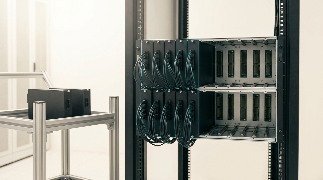
Sixteen bays, half of them plausibly still empty on any given day this product family exists — that is closer to the honest state of this technology in September 2026 than a finished rack humming at full deployment. The 32-terabyte figure is real, in the sense that Celestial AI’s own component disclosures make it arithmetically reachable, provided the unstated DDR5 topology behind those four controllers per module turns out to be denser than anything the same company has put a number to elsewhere. The optical bridge that routes connections through the middle of a package rather than only around its edge is a real, disclosed mechanism, not a rendering — it is the same shortage-of-edge problem NVIDIA’s own dual-die Blackwell package solves a different way, which is a useful sign that the underlying constraint this fabric is built to route around is a genuine one shared across the industry, not a problem invented to justify a product.
What is not yet real, in any sense a reader can verify, is the specific claim that gives this architecture its name: that reaching any point in a package with light, rather than only its perimeter with copper, turns thirty-two terabytes of mostly ordinary memory into something a die can treat as its own — cheaply enough, in energy terms, that the word “extension” is doing honest work rather than flattering one. That claim has an exact, nameable falsifier: a wall-plug power figure for the fabric alone, disclosed by whoever holds this technology now, or measured independently by whoever deploys it first. Marvell inherited the team, the tapeouts, and the spec sheet. It has not yet, in anything this search could find, inherited the obligation to publish the one number that would tell a reader whether “extension of the die” describes a new kind of memory system or a new name for an old one.
Marvell already sells custom accelerator silicon to hyperscale customers operating at exactly the fleet scale the amortization argument above needs to close in the fabric’s favor. Those deployments, not a spec sheet or a conference slide, are the plausible source of the first independent, deployed-at-scale power measurement this technology has ever had. Until one of them publishes it, or Marvell decides disclosure now serves its roadmap better than silence did before the acquisition, “extension of the die” stays exactly what the evidence in hand supports and no more: a real mechanism, a real product family with real tapeouts behind it, and an energy claim resting on a number nobody outside a design-review room has yet had to defend in public.