Nvidia Built a GPU with No HBM in It, on Purpose
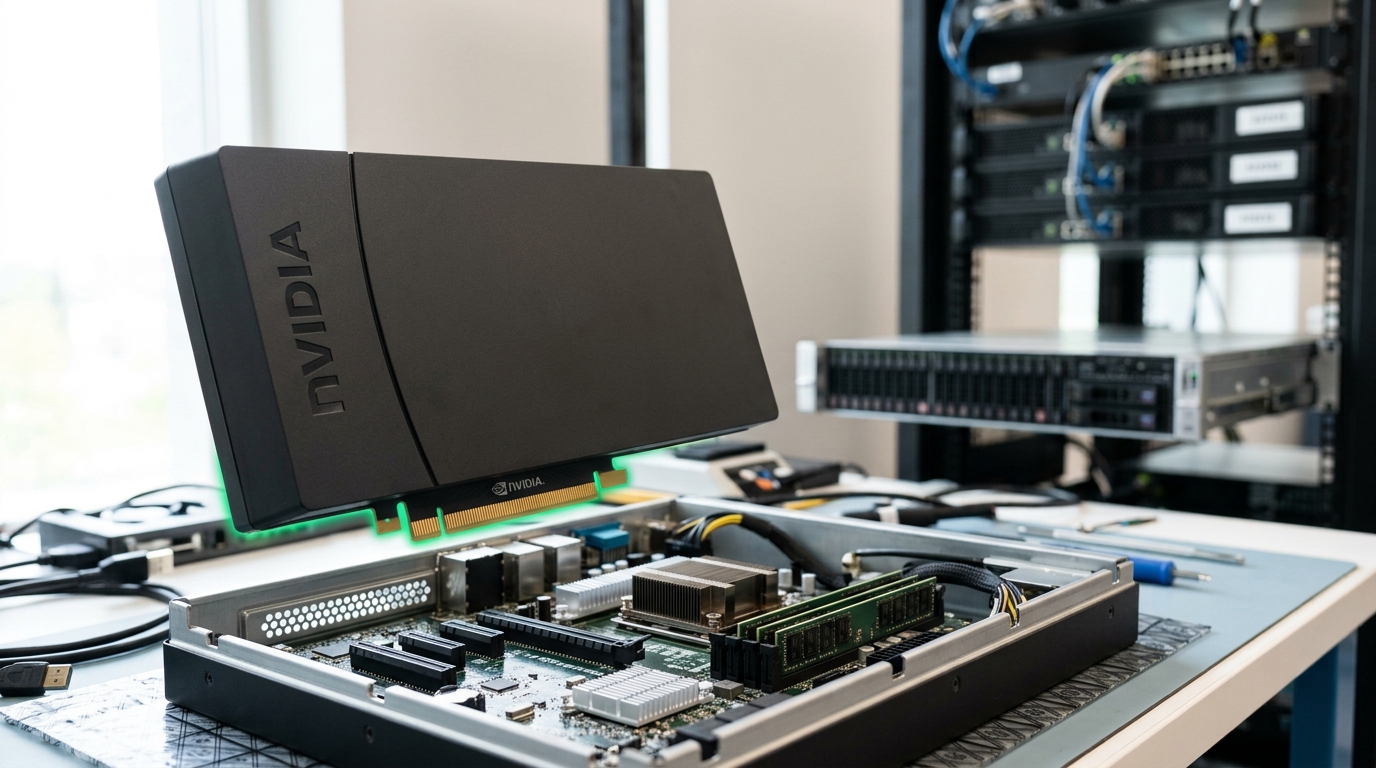
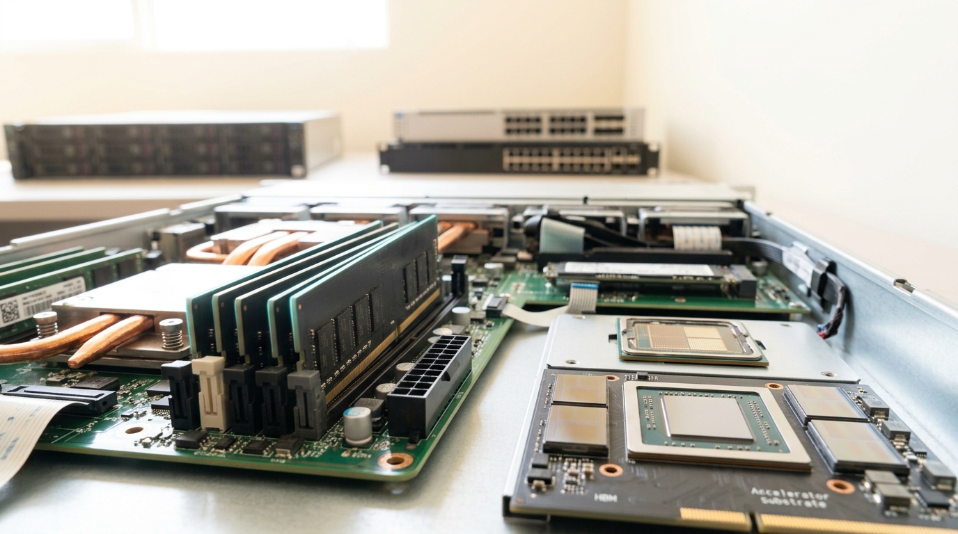
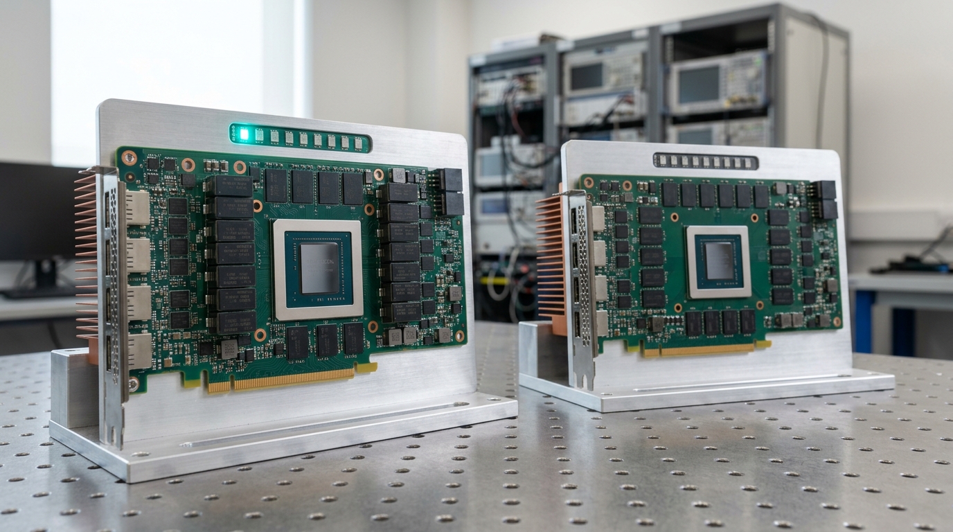
On September 9, 2025, at Nvidia’s AI Infra Summit, the company unveiled a data-center GPU with a memory subsystem that reads, on paper, like a mistake. Every other chip in Nvidia’s current lineup uses HBM — high-bandwidth memory stacked directly beside the compute die for the shortest, fastest path bytes can travel. The new chip, called Rubin CPX, uses GDDR7 instead: the same memory family found in gaming graphics cards, wired around a single monolithic die rather than the multi-die package the rest of the Rubin generation ships in [10]. Nvidia’s own numbers put Rubin CPX at up to 30 petaflops of dense NVFP4 compute against 128GB of that GDDR7 memory [10], moving data at roughly 2TB/s [9] — an order of magnitude less bandwidth than the 22TB/s HBM4 subsystem on the standard Rubin GPU shipping alongside it [7] [8].
A company that had just spent a decade telling the market that memory bandwidth is the thing standing between an AI accelerator and a faster future does not accidentally ship a bandwidth-starved chip into its flagship generation. It ships one on purpose, for a specific, nameable reason, or it does not ship one at all. This article’s claim is that the reason is visible in advance, in a number Nvidia has been quietly making larger for a decade: the ratio of tensor-core compute to memory bandwidth on its own data-center GPUs, tracked generation by generation from the 2016 Tesla P100 through 2026’s Rubin. That ratio does not wander. It rises, every single time a new architecture ships, and by the sixth generation it has grown so large — and grown unevenly enough between the two halves of a modern inference workload — that a single universal chip can no longer serve both halves well. Rubin CPX is what happens when Nvidia stops trying.
The obvious reading of a GPU with a tenth of its sibling’s bandwidth is that it is a cheaper, lesser part — a lower shelf in the product line, not a different kind of product. That reading survives about as long as it takes to notice that Nvidia is not selling Rubin CPX as an alternative to standard Rubin. It is selling both, in the same rack, wired together, each doing a job the other one is worse at. Explaining why a chip company would build two GPUs instead of improving one is the actual subject of this piece, and the explanation does not require guessing at Nvidia’s internal reasoning. It requires doing the arithmetic Nvidia’s own datasheets already make possible, generation by generation, and reading the trend the arithmetic produces.
None of the six specification sheets this argument rests on are proprietary. They are the same public datasheets any customer uses to plan a cluster purchase, cross-checked here against the two independent technical breakdowns of Rubin’s still-forthcoming specifications and against SemiAnalysis’s own accelerator-and-rack teardown of Rubin CPX specifically [1] [2] [3] [4] [6] [9]. What is original here is not the data. It is treating the ratio as a tracked quantity worth building a series out of, rather than a background fact each generation’s launch coverage mentions once and forgets.
The Ratio Doing the Actual Work: FLOPs per Byte, Not FLOPs per Second
Call it
The computation is arithmetic, not modeling. For each generation, take the dense — non-sparse — tensor-core throughput at whatever precision format that generation’s own datasheet treats as its headline AI number, and divide by the peak memory bandwidth of the same top-bin, data-center SKU. Dense, rather than the sparsity-inflated figure Nvidia’s marketing slides usually lead with, because structured sparsity requires a specific weight-pruning pattern that most dense pretraining and most prefill workloads simply do not use; the honest ratio for a real workload is the one silicon delivers without that assist. Pascal and Volta, the two oldest generations here, do not offer the choice at all — 2:4 structured sparsity is an Ampere-era feature — so for consistency every generation in this series uses the same dense convention, including the newer ones that could, in principle, report double.
That single methodological choice is worth stating plainly rather than burying in a footnote, because it is the reason this series’ numbers will look smaller than the ones a spec sheet or a press release usually quotes. A reader who has seen “H100: 3,958 teraflops” or “B200: 18 petaflops” attached to those chips is remembering the sparse figure. The dense number — 1,979 teraflops for H100’s FP8 tensor cores, 9,000 for B200’s FP4 tensor cores — is exactly half, and it is the number this piece uses throughout [4] [5] [6].
The reason arithmetic intensity is the right lens, rather than either raw FLOPs or raw bandwidth alone, is that a chip’s advertised compute figure is only ever a ceiling a given workload may or may not reach. Below a workload-specific threshold — the roofline model’s “ridge point,” the arithmetic intensity at which a chip stops being memory-bound and starts being compute-bound — throughput is capped by bytes moved, not by tensor-core count, and every FLOP of purchased silicon sitting past that ceiling is, for that workload, silicon paid for and not used. A rising
Six Generations, and the Number Never Once Fell
Here is the series, generation by generation, each row a real shipping data-center SKU at its top memory configuration:
| Generation | Announced | Dense AI precision | Compute | Memory bandwidth | FLOPs/byte |
|---|---|---|---|---|---|
| Tesla P100 (SXM2) | 2016 | FP16 | 21.2 TFLOPS | 732 GB/s HBM2 | ~29 |
| V100 (SXM2) | 2017 | FP16 Tensor Core | 125 TFLOPS | 900 GB/s HBM2 | ~139 |
| A100 (SXM4, 80GB) | 2020 | FP16 Tensor Core | 312 TFLOPS | 2,039 GB/s HBM2e | ~153 |
| H100 (SXM5) | 2022 | FP8 Tensor Core | 1,979 TFLOPS | 3,350 GB/s HBM3 | ~591 |
| B200 (Blackwell) | 2024 | FP4 Tensor Core | 9,000 TFLOPS | 8,000 GB/s HBM3e | ~1,125 |
| Rubin / VR200 | 2026 | FP4 Tensor Core | 33,300 TFLOPS | 22,000 GB/s HBM4 | ~1,514 |
Sources: [1] [2] [3] [4] [6] [7] [8] [9].
One of those rows deserves a specific note before the trend gets read off the table. Rubin’s compute figure is the one entry here that required reconciling a live disagreement rather than simply reading a datasheet: two independent GTC 2026 technical breakdowns each quote “50 petaflops of FP4” for Rubin, and they disagree with each other about what that number actually means — one describes it as a dense, non-sparse rating, the other states plainly that it already carries Nvidia’s sparsity-enabled Transformer Engine credit [7] [8]. SemiAnalysis’s own accelerator teardown resolves the disagreement: the dual-die Rubin GPU delivers 33.3 petaflops of dense FP4 and 50 petaflops with sparsity — a factor of roughly 1.5, not the 2x multiplier Blackwell’s own dense-to-sparse convention uses (72 dense to 144 sparse petaflops per HGX B200 GPU) — confirming the second reading and correcting the first [9]. This piece uses 33.3, not 50, for the same reason it used 1,979 rather than 3,958 for H100 two rows up — internal consistency mattered more here than the bigger number.
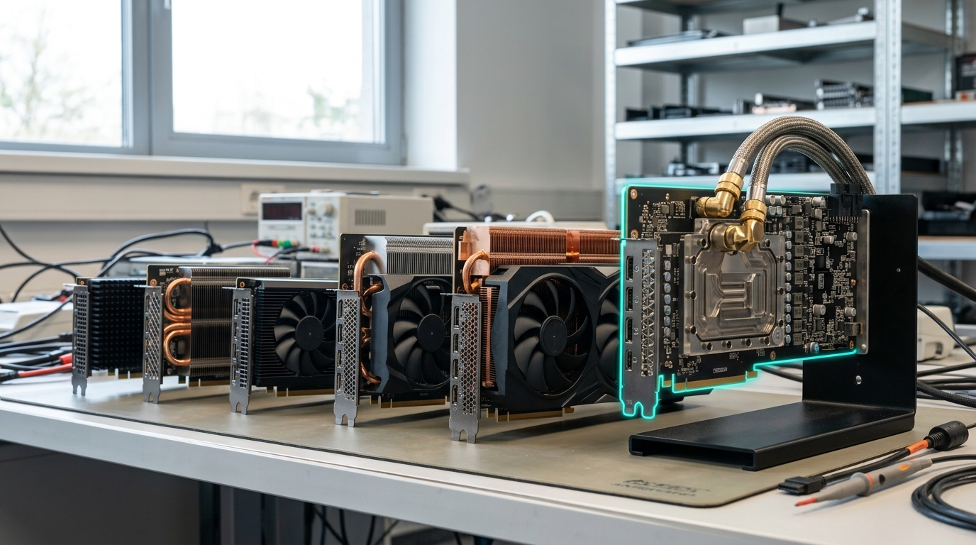
The trend itself does not need any hedge: 29, then 139, then 153, then 591, then 1,125, then 1,514. Never once, across six architectures and ten years, has the ratio fallen. That is the specific, falsifiable claim underneath everything that follows, and it is worth naming the condition that would break it: if any future Nvidia generation, or if a hypothetical seventh row inserted retroactively from a source this piece missed, showed dense compute growing slower than memory bandwidth for even one step, the “climbing ratio” claim would need to be withdrawn for that transition, not explained away. It has not happened yet, but the two smallest jumps in the table — Volta to Ampere, barely 10 percent, and Blackwell to Rubin, about 35 percent — show the climb is not a law of physics. It is a pattern Nvidia has kept choosing to extend, generation after generation, by making tensor-core throughput scale faster than HBM bandwidth every time a new memory standard becomes available. HBM4 is genuinely faster than HBM3e was. Nvidia’s FP4 tensor cores are faster than Blackwell’s by a wider margin still.
Each jump also has a name attached to it, and the names track a chip designer running out of one lever and reaching for the next. Pascal had no tensor cores at all; its FP16 throughput came from ordinary CUDA cores, and Volta’s nearly fivefold jump the following year was largely the arrival of dedicated Tensor Cores as a distinct execution unit, purpose-built for the matrix-multiply-accumulate pattern deep learning actually runs. Ampere’s own jump was the smallest in the table for a specific, identifiable reason: A100’s HBM2e bandwidth grew by roughly a third over V100’s HBM2, nearly keeping pace with a similarly modest compute increase in FP16, because Ampere’s real headline move — structured sparsity, and a new TF32 format for training precision — did not change the dense FP16 number this series tracks. Hopper’s jump back to nearly fourfold arrived with the Transformer Engine and FP8 as a first-class format, built explicitly because attention and feed-forward layers in transformers tolerate lower precision better than earlier architectures assumed; Blackwell’s second-generation Transformer Engine and native FP4 support repeated the same move a second time, at a point where FP8 headroom was no longer enough on its own. Every step down in numerical precision has been, functionally, a way to buy more arithmetic intensity without waiting for a slower-moving memory standard to catch up — and Rubin is the first generation in the table that does not do this. It ships no new precision tier below FP4; its compute gain over Blackwell comes from scaling the package itself, not from a cheaper number format, which is very likely why Blackwell-to-Rubin is the smaller of the two most recent jumps even with a genuinely new HBM4 standard supplying real bandwidth headroom alongside it. The easy lever — halve the precision, roughly double the throughput for free — is not infinite. Nvidia has now pulled it twice, at Hopper and at Blackwell, and Rubin’s own more modest climb is what the ratio looks like once that particular lever runs out and ordinary transistor and bandwidth scaling has to carry the trend alone.
Prefill Wants Arithmetic; Decode Wants Bytes; Nvidia Finally Built Both
A ratio that keeps climbing is, by itself, only half a story — a chip designer’s headache, not yet an explanation for a specific hardware decision. The other half is that large language model inference is not one workload with one arithmetic-intensity requirement. It is two, run back to back on every single request, and they sit at opposite ends of the roofline.
Prefill — reading a prompt and building its key-value cache before the model can generate a single output token — processes every token of the context in one large, parallel matrix multiplication. The same weight bytes get reused across every token in that batch, so arithmetic intensity scales with context length: a short prompt looks moderately compute-bound, and a long one, the kind Nvidia is explicitly selling Rubin CPX against — “million-token software coding,” in the company’s own description of the chip’s target workload — looks enormously so [10]. Decode is the opposite case in almost every respect. Generating each new token means reading the entire growing key-value cache back out of memory for a batch that, per request, is exactly one token wide; the compute per byte moved is small and the bandwidth demand is unrelenting. This publication’s own piece on serving a frontier model works through that batching-and-cache arithmetic in full, and this piece does not re-derive it — the point that matters here is narrower: SemiAnalysis states the resulting classification without hedging, in language this piece did not need to construct itself: “the prefill stage during inference tends to heavily utilize compute (FLOPS) and only lightly use memory bandwidth,” while “the decode phase… is always memory-bounded” [9].
Put the two halves of this piece together and Rubin CPX stops looking like a downgrade and starts looking like an answer to a question the ratio itself was asking. If standard Rubin, at roughly 1,500 FLOPs per byte, is already the highest-arithmetic-intensity general-purpose GPU Nvidia has ever built, and if decode’s own arithmetic intensity per request is a small, roughly constant number regardless of how fast the chip underneath it gets, then an increasing share of that 1,500-to-1 ratio’s headroom is compute the decode phase structurally cannot use — expensive HBM4 bandwidth sitting mostly idle while the chip waits on a workload that was never going to be compute-bound in the first place. Prefill, on the other hand, wants exactly what standard Rubin has too much of relative to its own needs: raw arithmetic, cheaply, in bulk, without paying HBM4’s premium for bytes it will barely touch. Rubin CPX’s own arithmetic intensity, on the published numbers, is not a modest step up from standard Rubin’s — it is roughly 6.6 times higher, on the same dense convention this piece has used throughout.
Nvidia’s own press release does not resolve this by itself. The company describes Rubin CPX as delivering “up to 30 petaflops” of NVFP4 compute without stating whether that figure is dense or already carries a sparsity credit [10]. But the same SemiAnalysis teardown that resolved standard Rubin’s own 33.3-versus-50 disagreement two sections back resolves this one too, in the same document: Rubin CPX delivers 20 petaflops of dense FP4 compute and 30 petaflops with sparsity [9]. Nvidia’s published “30 petaflops” is the sparse-inclusive figure, not the dense one this piece uses everywhere else. On the dense convention, Rubin CPX’s ratio against its roughly 2TB/s of GDDR7 bandwidth is about 10,000 FLOPs per byte — not a hedge between two readings, but the resolved figure, and it happens to surface something else worth stating plainly: Rubin CPX’s own dense-to-sparse multiplier is 1.5x, the same ratio standard Rubin uses, and neither matches Blackwell’s 2x. Nvidia’s own sparsity-credit convention shifted somewhere between the two generations — a reminder that a spec’s units can move under a vendor’s own numbers even while the headline term, “petaflops of FP4,” stays exactly the same.
The commitment is not a one-chip experiment, either. Rubin CPX ships inside a dedicated rack configuration, the Vera Rubin NVL144 CPX, which Nvidia describes as combining Vera CPUs, standard Rubin GPUs, and Rubin CPX GPUs into one system rated at 8 exaflops of AI compute, 100TB of fast memory, and 1.7 petabytes per second of aggregate memory bandwidth — a rack Nvidia claims delivers 7.5 times the AI performance of a GB300 NVL72 system built entirely from Blackwell Ultra’s own prior generation of universal chips [10]. A cost-segmented SKU sold quietly at a discount to whichever customer wants cheaper silicon does not usually get its own named rack architecture, marketed as a distinct product line alongside the flagship it is paired with. Nvidia built the rack around the split, not the split around a leftover die.
The Cheaper-Junk-Silicon Objection, and Why the Ratio Survives It
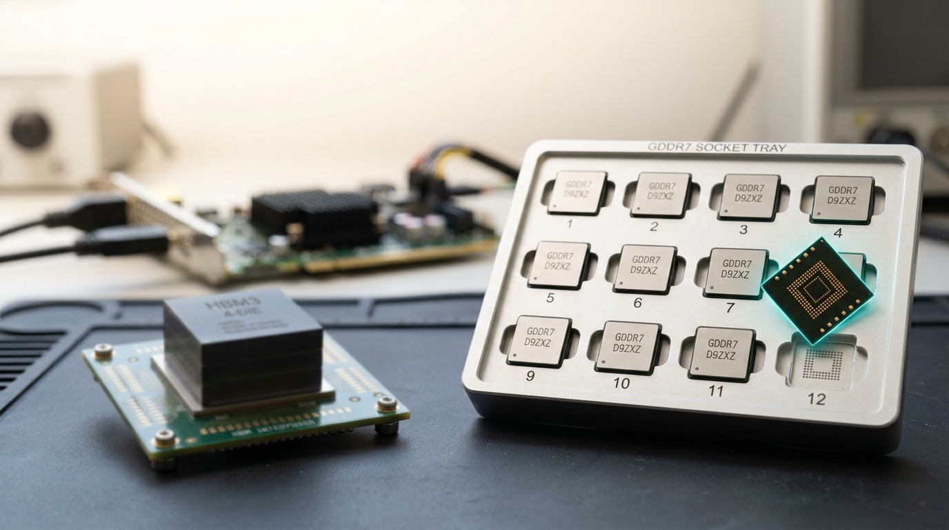
There is an entirely different, entirely reasonable story that explains a memory-poor Rubin CPX without any of the arithmetic intensity argument above: cost. GDDR7 is dramatically cheaper per gigabyte than HBM4 — SemiAnalysis puts the reduction at “more than 50%” — and a monolithic die is easier and cheaper to yield than the multi-die package standard Rubin ships in [9]. On this reading, Rubin CPX is not a response to arithmetic intensity at all. It is a margin-friendly SKU built from a cheaper bill of materials, sold into whatever workload will tolerate the resulting bandwidth shortfall, with the prefill-optimized framing supplied afterward as marketing rather than as the actual design driver. Chip companies have shipped cost-segmented parts and called them purpose-built before; there is no reason to assume Nvidia is above the same move, and the ratio computed above cannot, on its own, rule that story out.
What the ratio can do, and what a pure cost story cannot explain nearly as well, is predict which specific inference phase a cost-segmented chip should be aimed at, if the arithmetic-intensity story rather than the cost story is actually doing the design work. A chip built purely to be cheap has no principled reason to land on the compute-heavy side of the prefill/decode split rather than the bandwidth-heavy side — cheaper silicon could just as easily have been marketed at decode, which is the larger fraction of most serving budgets by request volume, if cost segmentation alone were the whole explanation. It was not marketed there. Nvidia’s own description of Rubin CPX names “million-token software coding and generative video” — long-context, prefill-heavy workloads specifically — as the target, and pairs it explicitly with standard Rubin’s HBM4-equipped decode role inside the same Vera Rubin NVL144 CPX rack rather than positioning it as a cheaper substitute for Rubin generally [10]. That is the discriminator this objection has to clear: the compute-heavy chip lands on the specific phase independently classified as compute-bound, not on an arbitrary or cost-convenient one. A coincidence is not impossible. It is a less likely reading than a designed one, once the independent classification of prefill as compute-bound and decode as memory-bound predates Rubin CPX’s existence by years rather than being invented to fit it.
The honest version of this section’s conclusion is not that the cost explanation is wrong. It is that cost and arithmetic intensity are not actually competing explanations here — they are complementary ones, and Nvidia had every reason to want both at once. A chip aimed at the compute-bound half of inference does not need expensive bandwidth it cannot use; building that chip out of cheaper memory is not evidence against the arithmetic-intensity story, it is close to the arithmetic-intensity story’s own prediction, restated as a bill of materials. Cost segmentation in chip design is common precisely because it usually tracks a genuine technical difference in what a given die is good at — a cut-down part with less cache or fewer memory channels is normally cheaper because it was already worse at the bandwidth-hungry jobs, not cheaper and then coincidentally worse at them. Rubin CPX fits that older pattern more than it fits a purely artificial market-segmentation story invented to extract extra margin from an otherwise identical die.
The version of the objection that would actually falsify this piece’s reading is narrower and more specific: if Rubin CPX, once shipping at volume in late 2026, turns out to be deployed predominantly for decode-heavy or mixed workloads rather than the long-context prefill role Nvidia is currently selling it for, the mapping this section defends collapses, and the chip really was just a cheaper SKU that got a convenient label.
Where the Next Break Sits, and What Would Prove This Wrong
Six generations of a climbing ratio, and one generation where the ratio finally climbed unevenly enough to force a second chip, suggests a question worth asking out loud rather than leaving implicit: does the split stop at two? I think it does not, and I want to be precise about why that is a proposal rather than an observation. Nothing in Nvidia’s public roadmap names a third specialized die for the generation after Rubin. What the six-generation series does show is that the pressure producing Rubin CPX — tensor-core throughput compounding faster than memory bandwidth, decade after decade, with no sign of the pattern breaking — has not stopped, and every prior attempt to serve a widening range of arithmetic-intensity requirements from one universal chip has eventually given way to a more specialized one. Pascal’s single die handled everything Nvidia sold in 2016. By Rubin, that same univocal role has already split in two.
The forward claim, stated as a proposal rather than dressed as a certainty: if the FLOPs-per-byte ratio for Nvidia’s next post-Rubin flagship continues climbing at anything close to its historical pace — and every generation in the table above has climbed, the slowest by ten percent and the fastest by nearly five times — the gap between what a maximally compute-bound inference phase needs and what a maximally memory-bound one needs will keep widening rather than closing, and Nvidia will face the same choice again: build one chip that serves both phases poorly, or build a second specialized part. Nothing about physics forces the second answer. Nvidia could instead choose to slow the compute-side climb, lean harder on in-network reduction or next-generation memory standards to close the gap from the bandwidth side, or simply accept a wider band of “good enough” compromise in a single universal die than the ratio’s own arithmetic would suggest. Those are real, available alternatives, not strawmen, and any of them would show up in public specifications the same way this piece’s own six rows did.
That is also this piece’s stated failure condition, not a hedge tacked on at the end but the actual test: if Nvidia’s next flagship generation after Rubin ships as one universal chip — no compute-heavy, memory-poor sibling, no further bifurcation — while the ratio computed from its own published specifications continues to climb at anything like its historical rate, the specific mechanism this piece proposes, that a widening arithmetic-intensity gap between inference’s two phases forces hardware bifurcation, is wrong, and the split visible in Rubin CPX today would need to be read as a one-generation event rather than the start of a trend. The six numbers in the table above are Observed, drawn straight from datasheets. The claim that they are still rising for a structural reason, not by coincidence, is Derived from them. The claim that this specific pressure, and not primarily cost, is what produced Rubin CPX is this piece’s own proposed reading, defended against its strongest competing explanation above. And the claim that a third specialized chip is coming is exactly what it is labeled here: a bet, with a stated way to lose it, not a prediction dressed up as an observation.