Seventy years is a long run for one body plan. From the first planar silicon transistors of the late 1950s to the finned and now gate-all-around transistors going into fabs in 2026, every mainstream logic chip has been the same basic design — a field-effect switch made of doped silicon, scaled smaller on a roughly two-to-three-year cycle — and for most of that run, scaling it smaller made it simultaneously faster, cooler, and cheaper per function. That triple coincidence is the actual content of “Moore’s Law”: not a law of physics, but a fifty-year run of one design’s dominance so complete that competing designs never got a foothold, because there was never a niche left over for them to win. Biology has a name for what happens when a dominant body plan’s advantage collapses and it stops out-competing everything else by default: not replacement by a single fitter successor, but radiation — several previously marginal lineages, each finding the one narrow niche where it now wins, none of them re-creating the old dominance on its own. This article argues that compute is now several years into exactly that radiation, that the fossil record is already legible in shipping products and published benchmarks, and that the popular shorthand for where it ends — “quantum will replace classical computing” — misreads the pattern almost as badly as an observer of the Cambrian radiation might have misread trilobites as a rehearsal for one later, superior arthropod.
CMOS Scaled on One Knob, and the Knob Broke Twice
The knob was Dennard scaling, and its mechanics were almost embarrassingly simple. Robert Dennard and his IBM colleagues showed in 1974 that if you shrank a transistor’s linear dimensions by a factor while proportionally shrinking its voltage, its power density stayed constant even as its switching speed went up — which meant each new process node could pack more, faster transistors into the same area and the same power envelope, essentially for free. For three decades that free lunch funded the entire consumer-electronics industry’s roadmap. Then, in a widely cited 2007 retrospective on Dennard’s own paper, Intel Fellow Mark Bohr marked the point at which the mechanism stopped working: threshold voltage and leakage current do not keep scaling down the way the other dimensions do, so below a certain size, shrinking a transistor further no longer holds power density flat — it raises it [5]. The clock-speed wall that followed is easy to date empirically, because it produced an unmistakable fossil in shipping hardware: desktop CPU clock speeds, which had climbed from single-digit megahertz to several gigahertz over three decades, essentially stopped climbing around 2005 and have sat in the same four-to-six-gigahertz band for two decades since, while the entire industry’s performance roadmap pivoted from “faster cores” to “more cores.” Dennard scaling’s death is the first extinction event in this story: the mechanism that had made the dominant body plan’s every generation strictly better than the last, for free, stopped applying to one of the two currencies it used to pay in.
The second extinction event took longer to become undeniable, because it hit the other currency — cost — and cost is harder to observe than clock speed. The historical version of Moore’s Law was never really about transistor count; it was about transistor count per dollar, and the economist Kenneth Flamm’s 2018 NBER analysis of the underlying price and cost data is explicit that the entire multi-decade run rested on “a 20 to 30 percent annual decline in the cost of manufacturing a transistor, on average, as long as it continued” [6]. Flamm’s empirical analysis of prices for the industry’s highest-volume products — memory chips, foundry-manufactured custom designs, and Intel’s own microprocessors — finds a clear slowdown in that decline relative to the historical trend, while noting that Intel microprocessor pricing shows some contrary evidence worth treating separately given the different competitive economics of that specific product line [6]. This is a more careful claim than the popular shorthand “cost per transistor has stopped falling,” and this article keeps that distinction: the data show a slowdown in the rate of decline across the industry’s dominant product categories, not a uniform flat line, and the exception in one specific product category is itself informative about why the slowdown is uneven. The industry’s own most recent roadmap corroborates the direction from the supply side. The IEEE’s International Roadmap for Devices and Systems, in its 2023 “More Moore” chapter, sets its own per-node cost target at “<30% more wafer cost – 15% less die cost for scaled die” [4] — a target that, unlike the roughly 30 percent linear-dimension shrink and better-than-doubling density gains the same roadmap still targets for performance and area, explicitly concedes that wafer cost is allowed to rise substantially from one node to the next, with only a modest net die-cost improvement expected to survive that rise. An industry roadmap conceding that cost, unlike density, is no longer expected to improve for free is itself a data point.
Two separate mechanisms, two separate collapses, a decade or so apart — and both point the same direction. A single scaling knob that once turned every currency compute cared about — speed, power, area, and cost — in the industry’s favor simultaneously now turns at most one or two of them at a time, and turns none of them as fast as it used to. That is not a minor engineering setback. It is the collapse of the specific advantage that let one body plan dominate every niche in a market for half a century, and it is the precondition for what evolutionary biologists call an adaptive radiation.
When a Body Plan Stops Scaling, Everything Uncompetitive Gets Its Moment
In evolutionary biology, a body plan does not usually lose to a single superior replacement. More often it loses its grip on every niche simultaneously, and what fills the vacancy is whatever was already sitting nearby, pre-adapted to conditions the dominant plan never had to compete under. The mammals that radiated after the non-avian dinosaurs’ extinction were not one new superior design; they were dozens of already-existing small-bodied lineages, each finding a niche — arboreal, burrowing, aquatic, gliding — that had been closed to them only because something else already held it more cheaply. The pattern has a name in evolutionary theory precisely because it recurs: release from a single dominant competitor does not produce a single new dominant competitor. It produces radiation, and radiation is not the temporary chaos before the next monopoly; in most of the historical cases evolutionary biology actually documents, radiation is the stable end state for a very long time afterward.
Compute’s version of this is legible in real hardware, not just as a rhetorical parallel. Every one of the lineages this article follows — three-dimensional stacking, photonic interconnect, neuromorphic chips, superconducting logic, reversible computing, quantum processors — has existed as a research topic for decades, in some cases longer than CMOS logic itself has been dominant. What kept every one of them out of the mainstream was never that they were bad ideas; it was that planar and finned CMOS, riding Dennard scaling and a falling cost curve, was strictly better on every axis a general-purpose logic chip is judged on, at a rate none of the alternatives could match while paying their own switching costs to unseat an incumbent. That is a classic case of what evolutionary theory calls competitive exclusion: two lineages competing for the identical niche do not coexist indefinitely, and the lineage with even a small compounding advantage — which is exactly what a two-to-three-year doubling cycle is — eventually excludes the other from that niche entirely, not because the excluded lineage was incapable, but because it never got the resources or the manufacturing scale to close the gap while the incumbent kept moving. Once the incumbent’s compounding advantage stops compounding, the same competitive-exclusion logic runs in reverse: lineages that were previously excluded from every niche can now win in the specific niches where their particular trade-offs, previously irrelevant next to CMOS’s all-around superiority, are actually the better trade to make.
This reframing matters because it predicts a specific, falsifiable shape for what comes next, and that shape is different from either of the two shapes most public discussion assumes. It is not “CMOS keeps improving as before” — the two extinction events in the previous section rule that out empirically. But it is also not “a new dominant design replaces CMOS the way CMOS replaced vacuum tubes and bipolar logic before it,” because a true successor would need the same thing CMOS itself had: a compounding advantage across essentially every workload, cheap enough to manufacture at incumbent volumes. Nothing in the lineages below is close to that. What the evidence instead supports, lineage by lineage, is specialization: each alternative winning the one or two niches where its own particular physics happens to be the right trade, while CMOS itself does not go extinct but instead becomes one lineage among several, still dominant in the niches — general-purpose logic at moderate power — where its trade-offs remain the best available. Dmitri Nikonov and Ian Young’s benchmarking study of candidate beyond-CMOS logic devices, conducted for Intel’s Components Research group and grounded in a uniform comparison methodology across more than a dozen device types, reaches exactly this conclusion from the device physics rather than from the evolutionary analogy: “we conjecture that future integrated circuits will still contain a majority of CMOS devices with a few other beyond-CMOS devices performing various specialized functions” [7]. That is radiation stated in engineering language rather than in biological language, and it is the frame this article now applies, lineage by lineage.
3D Integration Is the Only Lineage Already Filling CMOS’s Old Niche
Of every lineage in this radiation, three-dimensional integration is the one that has already gone mainstream, and it is worth being precise about why it is different from the others: it is not really a competitor to CMOS transistors at all. It is a change in how already-fabricated CMOS dies are combined, and it wins specifically the niche the two extinction events above made most acute — getting more function into a package without paying the ever-steeper wafer-cost premium of shrinking a single monolithic die further. The IEEE’s IRDS “More Moore” roadmap now tracks this transition explicitly as its own technology axis, distinct from ground-rule (linear-dimension) scaling: its 2023 edition projects “3D VLSI” — full monolithic or sequential three-dimensional integration, as opposed to simple die stacking — becoming the industry’s primary integration scheme after 2031, with complementary-FET (CFET) device architectures, which stack n-type and p-type transistors vertically atop each other rather than side by side, entering the roadmap for 2031 and reaching what the roadmap calls “5nm equivalent” node labeling by 2037 [4]. The roadmap is explicit that this is a response to the same cost pressure documented above, not an independent choice: it notes that after full-scale 3D VLSI integration is adopted, the industry will “further maintain the number of functions per unit cube” even as per-node linear scaling delivers diminishing returns on its own [4].
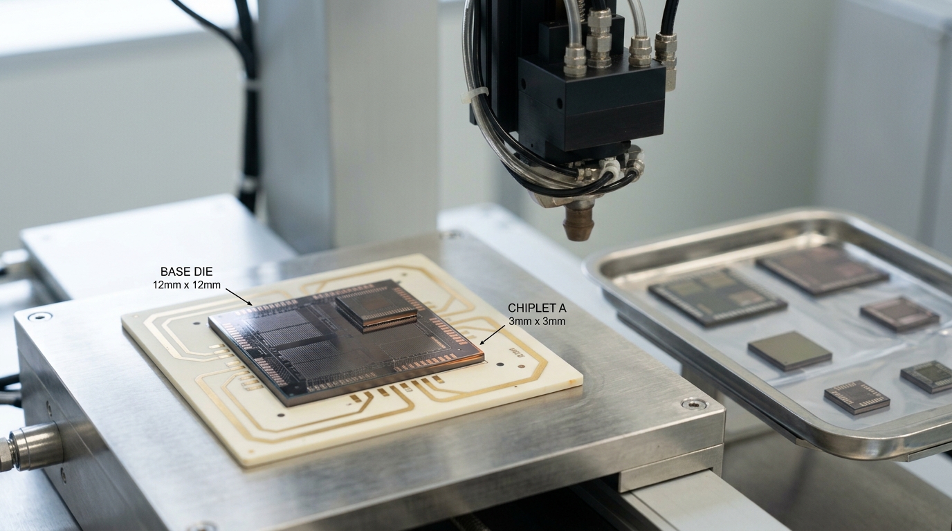
What makes 3D integration different from every other lineage in this article, and worth naming as an exception to the radiation pattern rather than an instance of it, is that it does not occupy a narrow niche next to CMOS — it occupies CMOS’s own former niche, general-purpose logic density, by attacking the problem from a direction Dennard-era scaling never had to use. Stacking two logic dies vertically and connecting them with a dense grid of through-silicon vias or, in the more advanced hybrid-bonding schemes the IRDS roadmap tracks, direct copper-to-copper bonding between wafers, adds a third spatial dimension to a scaling problem that had been treated as purely two-dimensional since the 1960s. This is precisely the kind of move evolutionary biology also documents: a lineage under competitive pressure does not always find a wholly new niche, and sometimes instead finds a new resource axis within its old one — vertical space in a forest canopy, in the biological case; the z-axis of a chip stack, in this one — that lets it keep occupying essentially the niche it always occupied, just organized differently. That is why chiplets and 3D stacking are the mainstream successor in a sense none of the other lineages below can claim: every major logic and memory manufacturer has already committed roadmap capital to this path, and the remaining questions are engineering execution — yield across bonded layers, thermal dissipation through a taller stack, the interconnect complexity of routing signals between tiers, all difficulties the IRDS roadmap itself flags as its hardest near-term and long-term challenges [4] — not whether the niche exists.
Photonic Interconnect Wins the Niche Electrons Are Bad At
Move a bit a few millimeters across a chip, and copper wires are close to optimal: cheap, easy to fabricate in the same process as the transistors, and fast enough that resistive and capacitive losses barely matter at that distance. Move the same bit tens of centimeters — between chiplets in a package, between accelerators in a rack, between racks in a data hall — and the physics inverts. A copper trace or cable driving a signal that far has to fight resistance and capacitance that scale unfavorably with distance, burning energy proportional to how far the electrons have to be pushed and how fast, in a relationship that has no equivalent penalty for a photon traveling down a waveguide or fiber, whose energy cost per bit is nearly independent of the distance traveled. This is not a claim that photonics is faster or cheaper than electronics in some general sense; it is a much narrower and more defensible claim that photonic interconnect wins one specific niche — long-haul, high-bandwidth communication between compute elements that are not the same die — precisely because that is the one job description where the physics that makes copper cheap at short range makes it expensive at long range.
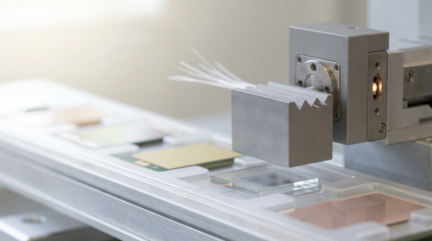
The demonstration that made this niche concrete rather than theoretical was a 2015 Nature paper from a MIT-Berkeley-Colorado collaboration, which built what its authors describe as a single-chip microprocessor that communicates directly using light, fabricated on an unmodified, commercially available 45-nanometer silicon-on-insulator CMOS process rather than a specialized photonics process [13]. The significance of that specific detail — an ordinary logic process, not a boutique photonics fab — is that it is the difference between a laboratory curiosity and a lineage with a plausible path to the same manufacturing volume as the CMOS logic it plugs into: if photonic input-output has to be built in its own separate, low-volume process, it stays a niche interconnect option for the most bandwidth-starved systems; if it can ride the same high-volume CMOS process as the logic it serves, its cost curve can in principle track the rest of the industry’s. A decade on, that path is exactly the one the industry has taken, with co-packaged optics — placing photonic engines directly in the same package as the switch or accelerator silicon they serve, rather than at the far end of a pluggable transceiver — now the subject of active high-volume manufacturing process work aimed specifically at data-center interconnect, the same niche the 2015 demonstration targeted. Photonic interconnect is not a competitor to CMOS logic in the way that framing might suggest; it is a lineage that only makes sense paired with CMOS logic, carrying the bits CMOS computes to wherever they need to go next, at the one length scale where light was always going to beat electrons.
Neuromorphic Chips Trade Throughput for a Different Currency
Every lineage discussed so far still computes the way CMOS logic always has: a global clock ticks, every active transistor in step with it switches whether or not its particular computation needs to happen that cycle, and the chip’s power draw is roughly proportional to its clock speed times its transistor count, regardless of how sparse or dense the actual useful work is. Neuromorphic chips reject that premise entirely, and in doing so open a niche that clocked, dense CMOS logic structurally cannot win: workloads where most of the “neurons” in a network are silent at any given instant, and where the interesting information is encoded in the sparse, irregular timing of the events that do occur rather than in a dense matrix of values updated every clock cycle.

Intel’s Loihi architecture is the most extensively documented example of this approach in the peer-reviewed literature. A comprehensive 2021 survey of Loihi’s results in Proceedings of the IEEE, co-authored by the architecture’s lead designers, characterizes the chip as an asynchronous, event-driven spiking-neural-network processor whose circuits only consume dynamic power when a spike actually needs to be routed or a synapse actually needs to be updated, in contrast to the clocked, dense-matrix style of computation that dominates both conventional CPUs and the GPUs used for mainstream deep learning [8]. That architectural choice defines the niche precisely: on workloads that are naturally sparse and event-driven — certain classes of real-time sensor processing, some forms of optimization and constraint satisfaction, adaptive control loops that spend most of their time near a steady state — an architecture that only spends energy when something changes has a structural advantage no amount of further CMOS density scaling can erase, because the advantage is not about transistor count or switching speed; it is about not switching at all when nothing is happening. On workloads that are naturally dense — the large matrix multiplications underlying most of today’s transformer-based AI systems — the same architectural choice is a liability rather than an asset, because dense computation has nothing sparse to exploit and pays the overhead of event-driven routing for no benefit. The IRDS roadmap itself frames neuromorphic and other emerging device technologies in exactly these terms, as niche additions rather than replacements: it projects “early adoption of Beyond CMOS technology and/or computing” around 2028 for specific applications, naming memristors “for neuromorphic applications” specifically, while continuing to project mainstream gate-all-around and CFET CMOS scaling as the platform for everything else [4]. That is the radiation pattern again, this time inside a single roadmap document: the incumbent design continuing to serve the niches it still wins, a beyond-CMOS lineage entering only where its different currency — near-zero idle power, event-driven sparsity — actually pays off.
Superconducting Logic Wins Only Where Someone Else Already Pays for Cold
Single-flux-quantum logic, the leading superconducting digital circuit family, switches using magnetic flux quanta trapped in superconducting loops rather than charge stored on a transistor’s gate capacitance, and the energy required to flip one of those flux quanta is small compared to the energy a room-temperature CMOS gate spends charging and discharging its load capacitance on every switch. A 2013 review by researchers at MIT Lincoln Laboratory, published in IEEE Transactions on Applied Superconductivity under the direct title “Energy-Efficient Superconducting Computing,” lays out exactly what this technology needs to actually deliver that efficiency at system scale: not just the switching-energy advantage of the logic gates themselves, but a full power budget that accounts for the fixed overhead of the cryogenic refrigeration plant the entire system depends on, since single-flux-quantum circuits only operate at liquid-helium temperatures near 4 kelvin [9].
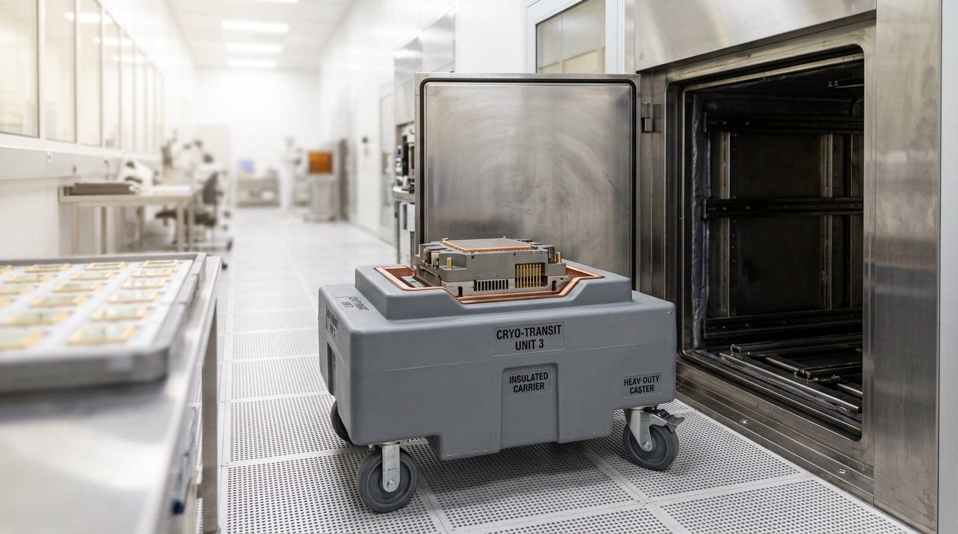
That fixed overhead is the whole story of why this lineage has stayed a niche for as long as digital superconducting logic has existed as a research field — decades longer than most of the other alternatives this article covers. A refrigeration plant capable of holding a meaningful amount of superconducting circuitry at 4 kelvin draws real, continuous power whether the logic inside is doing useful work or sitting idle, in a way that has no equivalent for a room-temperature CMOS server that can be powered down or throttled when idle. That structural fact defines the niche with unusual precision: superconducting logic only wins where a system is going to run at high, sustained utilization regardless — so the fixed refrigeration cost is amortized over enough useful switching to be worth it — and where the workload’s own energy budget is otherwise dominated by ordinary CMOS’s per-switch dissipation rather than by any fixed cost of its own. A dedicated, continuously running high-performance-computing cluster is a more plausible home for this lineage than a general-purpose data center whose load varies hour to hour, which is exactly the niche national research programs pursuing cryogenic computing have targeted rather than any attempt at a general-purpose replacement for CMOS servers. Superconducting logic is a clean illustration of a rule this article returns to below: an enormous switching-energy advantage on paper does not automatically translate into a winning niche, because the fixed cost of the environment a lineage needs in order to switch that efficiently has to be paid regardless, and only some workloads generate enough volume to make that payment worthwhile.
Reversible Computing Is the One Lineage Built to Cross a Floor, Not Approach It
Every lineage discussed so far competes on how close it can get to doing more with less energy per operation. There is a hard floor beneath all of them, derived not from engineering but from statistical mechanics, and it is worth stating precisely because the rest of this section depends on it. In 1961, the IBM physicist Rolf Landauer showed that any logically irreversible operation — one that destroys information, such as erasing a bit or overwriting one value with another without retaining a way to reconstruct the original — must dissipate a minimum amount of heat into its environment, because the entropy the erased information represented has to go somewhere, and the second law of thermodynamics says it can only go up [1]. The minimum energy that erasing one bit must dissipate, at absolute temperature
where
That bound is not a rough estimate awaiting refinement; it has been directly tested. A 2012 experiment reported in Nature, using a colloidal silica bead trapped in an optical potential rather than an electronic circuit, measured the heat dissipated while erasing one bit of information stored in the bead’s position and found it consistent with the Landauer bound within experimental uncertainty in the low-erasure-rate limit, the first experiment to test the bound this directly at the single-bit scale [2]. The bound is real, it has been measured, and every irreversible logic technology — which is to say every lineage covered in this article except the one this section is actually about — has to dissipate at least that much heat every time it erases a bit, no matter how exotic its switching mechanism is.
Measured against that floor, today’s mainstream logic is nowhere close, and the gap is large enough to state with confidence even given the uncertainty in any single measurement. The IRDS’s own 2023 logic-device electrical specifications table projects energy per switching event for a high-density logic cell at roughly 0.86 femtojoules in 2023, declining only to roughly 0.4 femtojoules by its 2037 projection even after the roadmap’s full projected run of gate-all-around and CFET architecture transitions [4]. A femtojoule is
Reversible computing is the one lineage in this article whose entire premise is closing that gap on purpose rather than as a byproduct, because it targets the actual mechanism the bound describes: it is only the destruction of information — not computation itself — that Landauer’s argument requires to cost energy. A logically reversible circuit, one built so that every output can in principle be run backward to reconstruct its inputs rather than discarding them, is not obligated to pay the Landauer cost at all, in principle, because it never actually erases the information the bound is about. A 2021 theoretical treatment by Michael Frank and Karpur Shukla, publishing in Entropy and building a rigorous derivation of Landauer’s bound from modern non-equilibrium quantum thermodynamics rather than from the heuristic arguments common in earlier literature, states the implication directly: “implementations of the alternative reversible computation paradigm can potentially avoid such losses, and thereby circumvent the Landauer limit, potentially allowing the efficiency of future digital computing technologies to continue improving indefinitely” [3]. Both instances of “potentially” in that sentence are the authors’ own hedge, not this article’s softening of their claim, and it is worth preserving exactly because it marks the real state of the field honestly: reversible computing is a theoretically sound path to bypass a real physical floor that binds every other lineage in this article, but it remains, as Frank and Shukla’s own framing acknowledges, a paradigm whose practical implementations are still being worked out rather than a solved engineering problem with a shipping product. No other lineage covered here — not 3D integration, not photonics, not neuromorphic chips, not superconducting logic — changes the fundamental relationship between erasing a bit and dissipating heat; each of them either reduces the constant of proportionality or avoids paying it in a different currency (superconducting logic’s small flux-quantum energies, neuromorphic computing’s sparsity), but only reversible computing proposes to make the erasure itself unnecessary. That is a categorically different kind of move, which is why this article treats it as the one lineage positioned to cross the floor rather than merely creep closer to it.
Quantum Processors Are a Niche Accelerator, Not a Successor
No lineage in this radiation attracts more overreach in popular discussion than quantum computing, and the overreach has a specific, identifiable shape: the claim that quantum processors are a more powerful successor to classical computers in general, coming for classical computing’s job the way CMOS came for vacuum tubes. That claim does not survive contact with what quantum processors are actually good at, and the people building them say so explicitly. John Preskill, who coined the term “NISQ” (noisy intermediate-scale quantum) for the current generation of quantum hardware in a widely cited 2018 paper, states the scope directly: current and near-future quantum devices will be useful tools for exploring specific problems, particularly many-body quantum physics, and “may have other useful applications,” but noise in quantum gates fundamentally limits the circuit depth and reliability available to them, which is precisely why they cannot yet take on the general-purpose, arbitrarily long computations classical hardware handles routinely [10]. That is a scientist working at the center of the field explicitly describing a niche, not a successor.
The clearest recent evidence that quantum error correction is finally improving fast enough to matter also, correctly read, reinforces the niche framing rather than undermining it. In December 2024, Google’s Quantum AI team announced results from a chip named Willow demonstrating that logical error rates fall exponentially as the number of physical qubits encoding each logical qubit increases — a milestone the field calls operating “below threshold,” which Google’s own announcement notes has been an explicit goal of the field since Peter Shor first introduced quantum error correction theoretically in 1995 [12]. The peer-reviewed paper behind that announcement reports the quantitative result precisely: logical error rate suppressed by a factor of
Three Named Futures for 2100, Each With What Would Prove It Wrong
None of the sources behind this article forecast to the year 2100; the IRDS roadmap’s own stated horizon is fifteen years, reaching only into the late 2030s, and the quantum and superconducting results above are current-state science, not century-scale forecasts. What follows, therefore, is this article’s own scenario construction, built by extrapolating each named source’s documented trajectory well past the horizon that source actually commits to — a distinction this section keeps explicit throughout, exactly because a claim about 2100 that quietly borrows a 2037 roadmap’s authority without saying so would misrepresent what that roadmap actually says.
Scenario one: continued heterogeneous integration, extrapolating the IRDS trajectory. The claim is that three-dimensional integration and chiplet-style heterogeneous assembly continue as the industry’s primary integration strategy well past the IRDS’s own 2037 horizon, with monolithic 3D stacking of increasingly diverse device and memory technologies — not merely repeated linear-dimension shrinking — doing most of the work that node-to-node scaling alone used to do. This scenario’s assumption is that the physical and economic logic the IRDS roadmap documents through 2037 — diminishing linear-scaling returns pushing the industry toward the vertical axis instead [4] — continues to apply because no alternative resource axis has yet been found, the same way it has applied continuously since the roadmap first began tracking 3D integration as a distinct technology axis. Its horizon is the end of 2045, chosen because it is roughly two roadmap cycles past the IRDS’s own explicit projections, a reasonable distance to extrapolate one documented trend without asserting knowledge of a second one. Its indicator is straightforward: continued publication of IRDS or successor-roadmap editions tracking increasing 3D-stack tier counts and decreasing per-function cost through further stacking rather than through linear shrinking. It is disconfirmed if, by 2045, the industry’s mainstream roadmap-setting bodies have stopped treating 3D stack height as an actively improving parameter — for instance, if tier counts plateau for two consecutive roadmap cycles rather than continuing to increase — which would indicate that stacking has hit its own diminishing-returns wall the way linear scaling did.
Scenario two: cryogenic and superconducting computing as a durable, bounded niche. The claim is that superconducting logic remains confined to a narrow set of applications defined by sustained, near-continuous high utilization — dedicated high-performance-computing clusters, certain classes of signal processing — rather than expanding into general-purpose data-center computing, because the fixed refrigeration overhead the 2013 MIT Lincoln Laboratory review identifies as the technology’s central system-level cost driver [9] does not scale away with further device-level efficiency improvements; it is a property of needing liquid-helium temperatures at all, not of any particular circuit design. This scenario’s horizon is the end of 2060, and its assumption is that no room-temperature or easily-achieved-temperature superconductor suitable for digital logic is discovered in the interim — a genuinely open empirical question in materials physics that this article does not attempt to forecast, and whose resolution in either direction would be the clearest possible falsifier. Its indicator is the deployment pattern of any superconducting-logic systems that do reach production: concentrated in continuously-run, high-utilization installations rather than general-purpose cloud infrastructure. It is disconfirmed if a room-temperature or near-room-temperature superconductor becomes commercially viable for digital logic, which would eliminate the fixed cryogenic cost that currently defines and bounds the niche, or alternatively if superconducting logic is still confined to research prototypes with no production deployment at all by 2060, which would indicate the niche is narrower even than this scenario assumes.
Scenario three: quantum processors as a permanent, expanding accelerator niche. The claim is that quantum processors follow the same trajectory as GPUs did relative to CPUs: never a replacement, but a permanent, increasingly capable accelerator attached to classical systems for the specific problem classes — quantum simulation, certain optimization and cryptographic problems — where quantum algorithms hold a proven advantage, with the boundary of that problem-class set expanding gradually as fault tolerance improves past the below-threshold milestone Google’s Willow chip demonstrated [11]. This scenario’s horizon is the end of 2050 and its assumption is that error-correction overhead continues improving at a pace similar to the exponential suppression already demonstrated, without asserting a specific timeline for when a fault-tolerant machine of any particular useful size arrives, since Preskill’s own account of the field explicitly declines to commit to such a timeline [10]. Its indicator is the growth rate of the documented set of problems with a proven, not merely conjectured, quantum speedup over the best available classical algorithm — a set that has grown slowly and been revised downward more than once in the field’s history as classical algorithms improved to close gaps once thought to require a quantum computer. It is disconfirmed if, by 2050, that documented problem set has not grown meaningfully beyond its current scope despite continued hardware scaling, which would indicate that error correction alone, absent new algorithmic advantage, does not translate into an expanding niche the way this scenario assumes.
Compute in 2100: An Ecosystem Sharing Fabs, Not a Successor Species
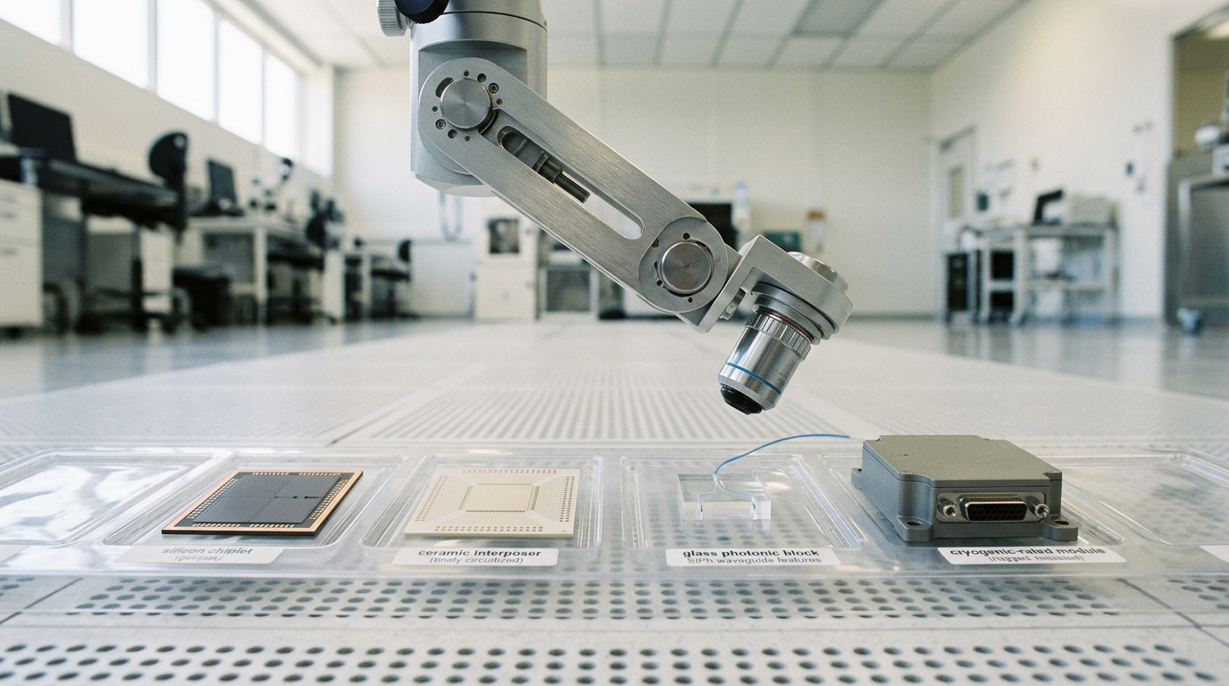
Put the three scenarios together, and the honest picture of compute at the end of this century is not a single winning architecture, any more than the honest picture of a forest is a single winning tree species. It is an ecosystem: CMOS logic, radically reorganized in three dimensions but still recognizably CMOS at the device level, doing the general-purpose work it has always done best; photonic interconnect carrying that logic’s bits across every distance longer than a single chiplet can economically bridge in copper; neuromorphic chips handling the specific sparse, event-driven workloads that dense clocked logic was never well suited for regardless of how small its transistors got; superconducting logic occupying the narrow, continuously-loaded niche where its cryogenic overhead is worth paying; and quantum processors, if the third scenario above holds, doing the same job for an expanding but still bounded set of problems that GPUs already do for dense linear algebra. None of these lineages is trying to become universal, and none of the evidence assembled in this article supports betting that any of them will. The extinction event was real — Dennard scaling did collapse in the mid-2000s, and the cost curve that funded seventy years of one body plan’s dominance has genuinely slowed. But an extinction event does not produce a new king of the hill on the far side of it nearly as often as popular science writing assumes; it produces the kind of radiation this article has traced lineage by lineage, and the correct question for a reader checking back on any of these claims decades from now is never which lineage won, but which specific niches each one actually ended up holding, and whether the boundaries of those niches moved in the direction this article’s scenarios said they would.