The bottleneck that isn’t where the headlines point
Coverage of AI hardware supply overwhelmingly focuses on the transistor: process node, die size, transistor density, yield. Those numbers matter, but by mid-2026 they were no longer the constraint that determined how many accelerators actually shipped. Multiple independent reports from TSMC’s own Q2 2026 earnings converged on the same point: CoWoS advanced-packaging capacity, not wafer starts, is the binding constraint on AI accelerator output [1]. This briefing works through why that is, with the numbers behind it.
What CoWoS actually is, briefly
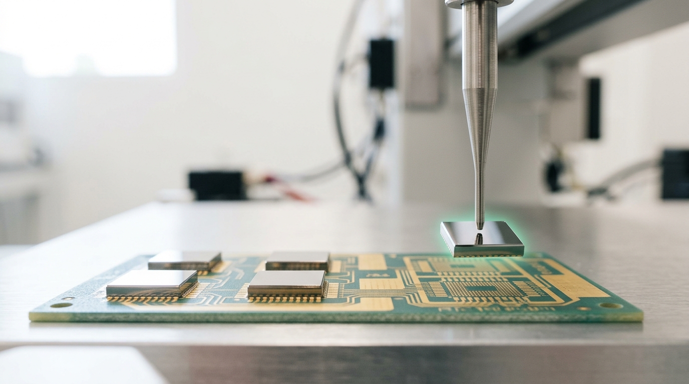
Chip-on-Wafer-on-Substrate is the packaging process that takes a finished logic die and one or more HBM memory stacks — each manufactured separately, by different processes, often by different companies entirely — and integrates them onto a shared silicon interposer and package substrate. Every modern AI accelerator that pairs a large logic die with high-bandwidth memory needs this step or something functionally equivalent to it. The logic die can be finished and sitting in inventory; the accelerator does not exist as a sellable product until packaging is done.
The capacity math
TSMC’s 2026 capital expenditure guidance allocates 10-20% of a $60-64 billion budget to advanced packaging — a meaningful sum, but a fraction of the 70-80% going to leading-edge process capacity [3]. Advanced-packaging capacity is reported growing at over 80% CAGR, an aggressive expansion rate on its own — but it is expanding from a much smaller base than wafer fabrication capacity, and packaging tools cannot simply be added at the same pace as lithography scanners, because the bonding, interposer, and substrate supply chains each carry their own separate capital and qualification cycles.
At first glance, an 80% packaging-capacity growth rate sitting above the 70% wafer-capacity growth rate looks like packaging is not the constraint. The reconciliation is in the base: packaging capacity started 2026 far smaller relative to demand than wafer capacity did, because demand for HBM-integrated accelerators grew faster than anyone provisioned for as recently as 2024. A higher growth rate from a smaller starting base can still leave an absolute shortfall wider at the end of the year than at the start — which is exactly what the reporting on customer allocation disputes suggests is happening in practice [4].
Demand side: what packaging capacity has to serve
Hyperscaler capital expenditure — the demand pulling on this exact packaging capacity — reached roughly $725 billion in combined 2026 guidance across Microsoft, Google, Amazon, and Meta alone, up 77% from 2025 [5]. Nvidia’s own reported visibility into $500 billion in combined Blackwell and Rubin revenue through the end of calendar 2026 gives a sense of the volume of individual packaged units that figure implies [8]. Custom ASIC shipments — Google TPU, Amazon Trainium, Microsoft Maia, and the rest — are growing at 44.6% year-over-year, nearly triple the 16.1% growth rate of merchant GPUs, and every one of those ASIC designs also needs advanced packaging, adding a second, faster-growing source of demand on the same constrained set of production lines [7].
| Layer | 2026 growth rate | Constraint type |
|---|---|---|
| Leading-edge wafer capacity (N2/A16) | ~70% CAGR | Capital-intensive, long lead time, but scaling |
| Advanced packaging (CoWoS/SoIC) | ~80% CAGR from a smaller base | Widest reported allocation disputes |
| Custom ASIC shipments | ~44.6% YoY | Adds demand on the same packaging lines |
| Merchant GPU shipments | ~16.1% YoY | Slower-growing, but from a much larger base |
Who actually captures the capacity
Reporting on 2026 CoWoS allocation describes a customer list large enough that no single buyer, including Nvidia, receives an open-ended share — capacity is explicitly divided among competing accelerator programs each quarter [4].
That allocation process is, in effect, the real rationing mechanism for the AI accelerator market in 2026: a design can be finished, yielding well, and still face a shipping delay set by a packaging-line queue rather than by anything wrong with the chip itself. TSMC’s response — the $265 billion Arizona commitment, including packaging capacity intended to eventually offer a complete domestic wafer-to-package chain — is a direct answer to this specific constraint, not a general capacity expansion [2]. Outside TSMC’s own lines, OSAT packaging specialists led by ASE Technology (reported at roughly 44.6% share of the top-10 advanced-packaging market) and Amkor are also expanding advanced-packaging capability, though neither yet offers CoWoS-class integration at TSMC’s scale [6].
The forecasting implication
Any 2026 or 2027 AI accelerator supply forecast built purely from wafer-capacity and process-yield assumptions will systematically overstate how many units actually reach customers, because it is missing the slower-moving constraint. The more reliable forward indicator is TSMC’s own advanced- packaging capex share and the specific capacity-allocation commentary that accompanies each quarterly earnings report — both of which say more about 2027 AI accelerator supply than any individual chip’s benchmark result does.