Before “accelerator” was a category
For most of computing history, the chip that did arithmetic and the chip that drew pictures were on a collision course only by accident. The processor family that would eventually train and serve the largest models on Earth started as a peripheral built to fill a video buffer, not to fit a matrix into memory. AI accelerator architecture does not begin at a founding moment invented for the purpose. It begins with people who wanted floating-point throughput for something other than pixels, found a commodity part that had more of it than any CPU on the market, and spent years bending a graphics pipeline into a shape it was never designed to hold.
That improvisation left fingerprints on every generation that followed. Routing an unrelated computation through hardware built for something else — vertex transforms standing in for physics, texture lookups standing in for table reads — is the direct ancestor of the general-purpose GPU compute model, which is the direct ancestor of the dedicated matrix engine, which is the direct ancestor of the systolic array inside a modern accelerator die. None of those later, cleaner abstractions had to exist. They exist because researchers spent years proving, the hard way, that the underlying hardware was worth formalizing.
This history follows that formalization in the order it happened, dated and sourced at each step: the shader-era workaround period, the 2006 arrival of a real general-purpose programming model, the 2012 result that made the whole approach urgent, the memory and packaging changes that quietly became as important as the arithmetic, chips built around one operation rather than a general instruction set, the startup wave that tested alternative bets, and the systems-scale architecture running today.
Borrowed hardware: shader-era GPGPU
By the mid-2000s, commodity graphics chips had become, almost by accident, the densest floating-point hardware a researcher could buy without a supercomputer allocation. A 2005 state-of-the-art report from Owens and six co-authors, later expanded into a widely cited journal survey, documented the resulting research movement under the name general-purpose computation on graphics hardware, or GPGPU [1]. The report’s own numbers explain the appeal: contemporary GPU floating-point performance had been compounding at roughly 1.7 to 2.3 times per year, against a yearly rate of about 1.4 times for CPU performance over the same period, a gap the authors attributed to the highly parallel, throughput-oriented design GPUs had already committed to for graphics reasons [1].
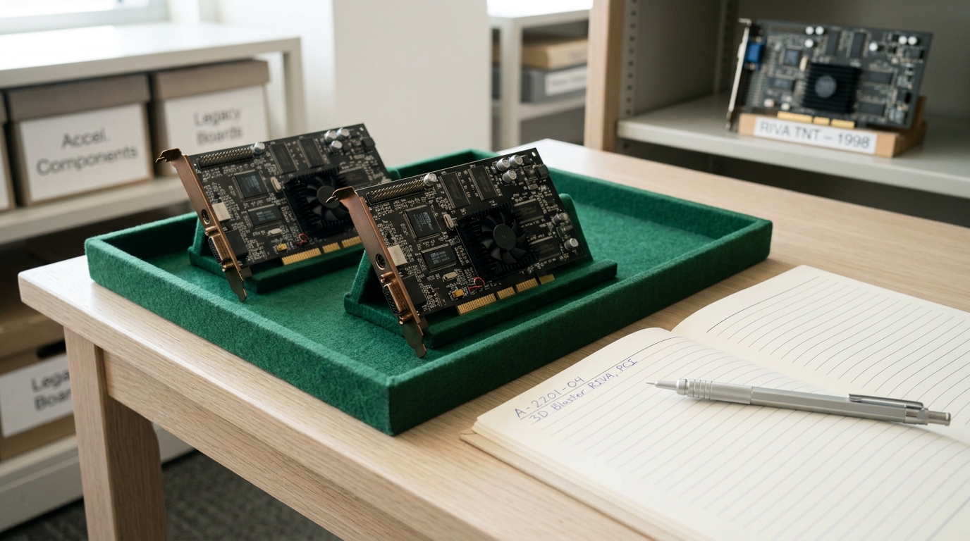
The catch was that none of this throughput was available through anything resembling a general-purpose instruction set. A GPU in 2005 executed vertex and pixel shader programs against a fixed graphics pipeline; researchers who wanted to run a physics simulation or a linear solver had to disguise it as a rendering job, encoding data as texture maps and expressing computation as shader code that happened to produce numerically useful output as a side effect of drawing something. Owens and colleagues catalogued this technique in detail, aiming to describe the general-purpose computation techniques being mapped onto graphics hardware for an audience of researchers who would build the next generation of GPGPU applications [1]. The survey is itself a marker of how far the workaround had spread by 2005: it existed because enough labs had independently converged on the same disguise that the technique needed collecting rather than reinventing in each lab.
What the shader-era approach lacked was a programming model that treated the GPU as a computer rather than a renderer that could be tricked. Every kernel had to be re-expressed as graphics primitives; every data structure had to fit inside a texture; and the class of programmer who could do this well was drawn from computer graphics, not from the scientific-computing or, later, machine-learning communities the hardware would eventually serve. That mismatch is what the next step in this history was built to remove.
2006: CUDA and the unified architecture
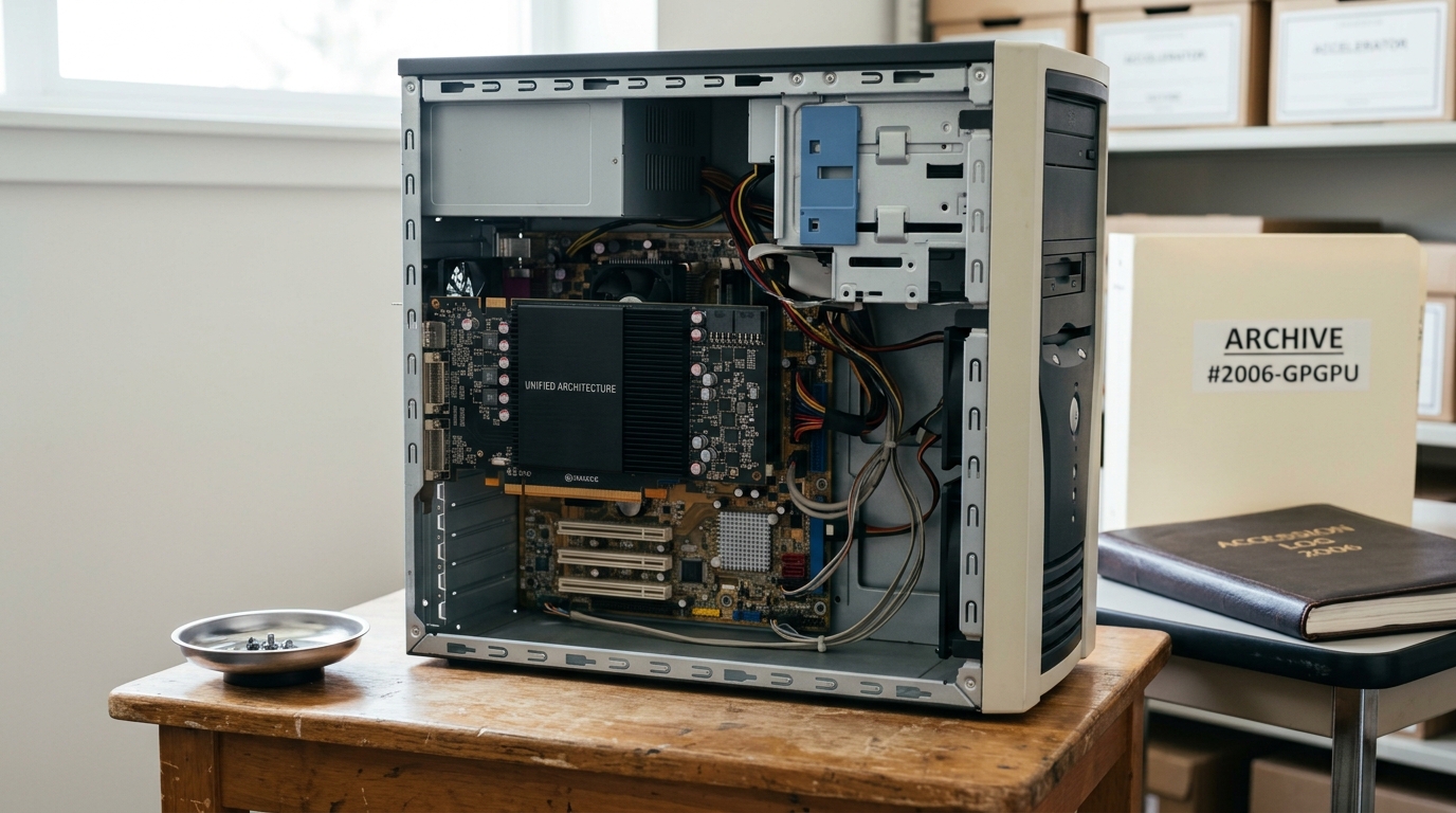
The formal starting point most standard histories of GPU computing settle on is dated precisely in the peer-reviewed record. Lindholm, Nickolls, Oberman and Montrym, writing in IEEE Micro in 2008, describe NVIDIA’s Tesla architecture as having been “introduced in November 2006 in the GeForce 8800 GPU,” where it unified the previously separate vertex and pixel processors “and extends them, enabling high-performance parallel computing applications written in the C language using the Compute Unified Device Architecture (CUDA) parallel programming model and development tools” [2]. That single architectural move — collapsing two specialized pipelines into one general, massively multithreaded processor array, and exposing it through a C-like language rather than a shader compiler — is the moment a graphics chip became, formally and officially, a general-purpose parallel computer that happened to also render graphics.
The same paper’s account of what came before is useful because it was written by the architects themselves and shows how incremental the change actually was. The authors trace fixed-function GPUs back to the GeForce 256 in 1999, note that the GeForce 3 introduced the first programmable vertex shaders in 2001, that the Radeon 9700 added a programmable pixel-fragment processor in 2002, and that Microsoft’s Xbox 360 shipped an early unified processor design in 2005, a year before Tesla brought unification to a PC GPU [2]. Unification was the last step in a six-year convergence the authors describe as driven by load-balancing inefficiency between separately provisioned vertex and pixel hardware.
What CUDA changed for the GPGPU researchers documented above was not the silicon’s raw throughput, which had already been climbing for years, but the cost of reaching it. A texture-disguised shader kernel and a CUDA kernel could in principle run on adjacent hardware generations, but only one of them could be written, debugged and maintained by someone without a graphics background. That accessibility is what let the technique leave the small circle of researchers Owens and colleagues had been writing for and reach the machine-learning community within a few years.
2012-2014: the pivot, and the library that followed it
The event conventionally credited with making GPU computing indispensable to machine learning, rather than merely useful to it, is dated to a single NeurIPS submission. Krizhevsky, Sutskever and Hinton’s 2012 paper on classifying ImageNet with a deep convolutional network states its hardware plainly: “our network takes between five and six days to train on two GTX 580 3GB GPUs” [3]. The network — eight learned layers, sixty million parameters, six hundred and fifty thousand neurons — won the 2012 ImageNet Large Scale Visual Recognition Challenge with a top-5 error rate of 15.3%, against 26.2% for the next-best entry, a margin the authors attribute in part to a “highly-optimized GPU implementation” of two-dimensional convolution applied to a network too large to train practically on hardware available to earlier competitors [3].
The paper is worth reading as an engineering document as much as a modeling one, because its authors are explicit that the result was hardware-gated, not idea-gated: convolutional networks with roughly this structure had existed for years, but the size that made them competitive on ImageNet had been, in their words, prohibitively expensive to train until hardware fast and cheap enough became available. Two consumer graphics cards, run for the better part of a week, is a modest footprint by later standards, but it was the specific pair that made the case. Within two years, the industry’s response had produced its own dedicated software layer. NVIDIA engineers Chetlur, Woolley, Vandermersch, Cohen, Tran, Catanzaro and Shelhamer released cuDNN in 2014, describing it as a library of GPU primitives built to fill a gap the high-performance-computing community had already solved with BLAS but that deep learning had not: reusable, optimized implementations of the convolution and pooling operations every framework was independently reimplementing by hand [4]. Their own measurement of the library’s effect, integrated into the Caffe framework of the period, was a 36% throughput improvement alongside reduced memory consumption on a standard model [4].
The sequence matters more than either event alone. AlexNet showed that a big enough network, trained on a big enough dataset, on hardware fast enough to make the experiment tractable, produced results qualitatively better than what preceded it. cuDNN showed the industry was prepared to invest in making the underlying primitives — not applications, not models, the convolution kernel itself — shared, maintained infrastructure rather than something every lab reinvented. That is the point at which GPU computing for neural networks stopped being a research curiosity and became a supply chain with a vendor at the center of it.
Packaging becomes a co-design decision
While the software and modeling side of the field was absorbing AlexNet’s implications, a quieter change was underway in how the memory beside the die got there. The mechanism that would eventually let accelerators feed arithmetic units fast enough to matter had two separate origins, one in advanced packaging and one in memory standardization, and both predate the deep-learning boom that would make them essential.
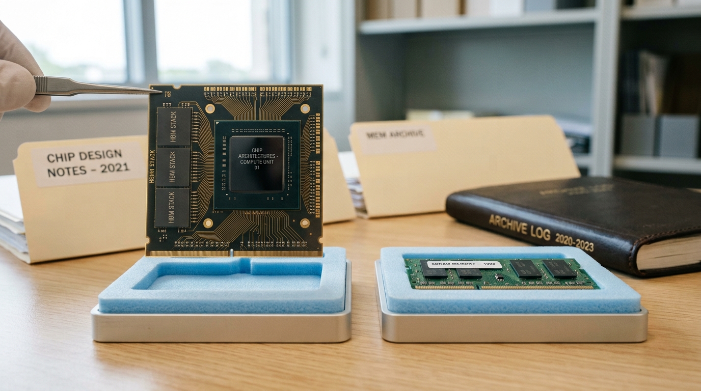
TSMC’s own account, in an October 2012 press release, describes tape-out of “the foundry industry’s first CoWoS test vehicle” integrating a JEDEC Wide I/O mobile DRAM interface, a chip-on-wafer-on-substrate assembly the company reported had reached the pilot production stage and that achieved more than 100 gigabits per second of DRAM bandwidth at low power by placing logic and memory on a shared silicon interposer rather than routing between them across a conventional circuit board [7]. That announcement predates any AI accelerator by half a decade; CoWoS was built to solve a mobile and FPGA packaging problem, and the AI accelerator industry later adopted an already-maturing platform rather than commissioning a new one.
The memory side followed a similar path. NVIDIA research scientist Mike O’Connor’s June 2014 presentation to The Memory Forum records that JEDEC adopted the High Bandwidth Memory specification, JESD235, in October 2013, with initial work on the standard having started in 2010 — three years of standardization before the specification existed as an approved document [5]. The presentation frames the standard’s purpose in terms any modern accelerator engineer would recognize: exploiting the large number of signals available through die-stacking for high bandwidth, reducing the energy cost of moving data across an interface, and letting a memory controller reach a higher fraction of theoretical peak bandwidth than a conventional off-package interface allowed [5].
The first product to ship with this new class of memory was a graphics card, not an AI chip. AMD’s own press materials, dated June 16, 2015, describe the Radeon R9 Fury X as “the world’s first HBM-powered graphics card,” built around the GPU AMD had codenamed Fiji [6]. That framing is a vendor’s own claim about its own product, but the underlying sequence is externally verifiable: a packaging platform matured in 2012, a memory standard was ratified in 2013, and the first commercial part combining them shipped in 2015 — three years of standards and manufacturing work that had nothing to do with neural networks, completed just in time for an industry that needed exactly this combination to feed its arithmetic units.
None of these three milestones was originally justified by AI. Wide I/O mobile DRAM, JEDEC’s stacking standard, and a gaming GPU were the proving ground; the AI accelerators built a few years later arrived once both had already been through a separate industry’s shakedown cruise.
2017: Google builds a chip around one operation
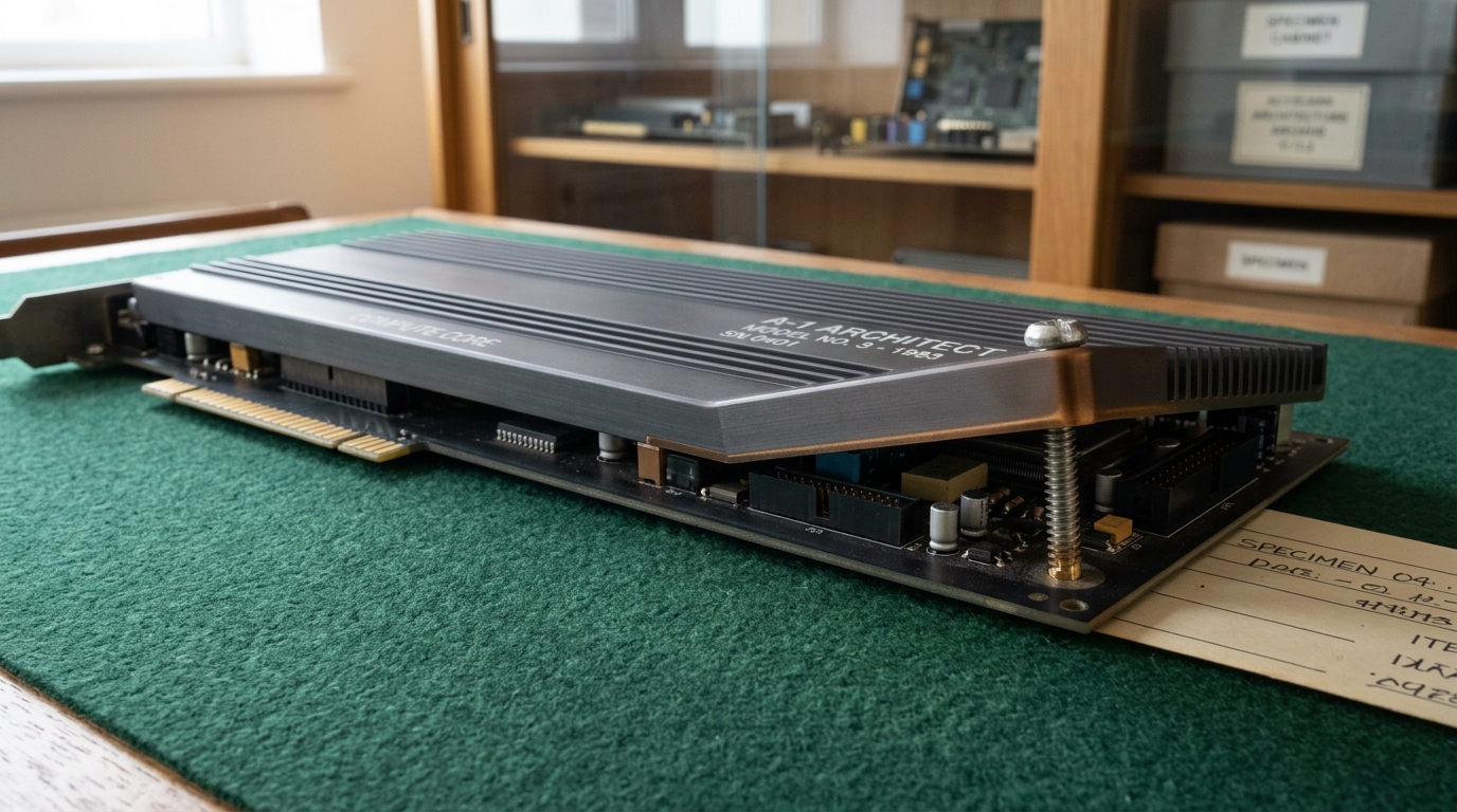
The clearest documented case of a chip designed from first principles around neural-network arithmetic, rather than adapted from a graphics processor, is Google’s first Tensor Processing Unit. Jouppi and a large team of co-authors, presenting at the International Symposium on Computer Architecture in Toronto in 2017, describe its computational core as “a 65,536 8-bit MAC matrix multiply unit that offers a peak throughput of 92 TeraOps/second,” trading the flexibility of a general instruction set for an array purpose-built to perform one operation, matrix multiplication, at very high density [8]. Measured against the CPUs and the contemporary GPU deployed alongside it in Google’s own datacenters, the paper reports the TPU running “on average about 15X - 30X faster,” with a TOPS-per-watt advantage of roughly “30X - 80X” [8].
Those comparison figures are the authors’ own benchmark results against their own choice of contemporary hardware, and should be read as such rather than as a portable, vendor-neutral ranking — a caveat this history returns to below. What is more durable than the specific multiplier is the design decision the paper documents: a chip whose entire arithmetic core exists to perform one kind of operation, at the expense of everything a general-purpose processor is normally asked to do well. A GPU descended from a graphics pipeline retained years of accumulated general-purpose flexibility even after CUDA and cuDNN made that flexibility accessible to machine-learning workloads; a TPU designed after AlexNet’s implications were understood did not carry that inheritance and could commit its die area entirely to the operation the field had already identified as dominant.
The paper contains one further result worth treating as structural rather than a footnote: the authors report that substituting the memory system of a contemporary GPU for the TPU’s own, with no change to the arithmetic array itself, would have roughly tripled achieved throughput on their workloads [8]. A chip built entirely around a matrix-multiply array was, by its own designers’ account, still bound more tightly by its memory than by its arithmetic — a finding that anticipated, in a single 2017 datapoint, the memory-bandwidth-centered design pressure that dominates the rest of this history.
2017: NVIDIA answers inside the GPU
The same year Google’s TPU paper reached ISCA, NVIDIA shipped an architecture that answered the same problem from inside the general-purpose GPU line rather than by building a separate chip. NVIDIA’s own Tesla V100 GPU architecture whitepaper, dated August 2017, documents the Volta generation’s central addition: a dedicated Tensor Core unit, distinct from the GPU’s existing general-purpose CUDA cores, built to perform 4x4 matrix-multiply-and-accumulate operations directly in hardware rather than as a sequence of general instructions [9]. The whitepaper presents this as the architecture’s headline capability and pairs it in the same document with the adoption of second-generation High Bandwidth Memory, HBM2, as the GPU’s on-package memory system [9].
The pairing is the point. Volta did not treat the matrix unit and the memory system as separate problems solved on separate schedules; the same 2017 architecture that introduced a dedicated matrix-multiply core also adopted the HBM standard traced to its 2013 JEDEC ratification two sections above, arriving in a general-purpose GPU two years after the same memory class had first shipped on a gaming card [9] [6]. Where Google’s TPU built a chip around the matrix operation from a blank sheet, NVIDIA’s answer grafted a comparable matrix unit onto an architecture that retained its general-purpose shader cores, memory controllers and existing CUDA software ecosystem — a different bet on the same observation that dense matrix multiplication justified dedicated silicon.
That the two largest AI accelerator efforts of 2017 converged, independently, on the same conclusion — a dedicated matrix-multiply array paired with stacked high-bandwidth memory — is itself a data point. Neither company borrowed the other’s chip design; both arrived at structurally similar answers because the arithmetic-to-bandwidth ratio of dense matrix multiplication was, by 2017, a well-understood constraint rather than a novel discovery.
2018-2020: the startup wave and the hyperscaler chip
Once two of the industry’s largest companies had committed to purpose-built matrix hardware, capital followed into startups betting on more radical departures from the GPU template, alongside the first hyperscaler-designed silicon built outside the two companies already discussed.
Amazon Web Services moved first among the hyperscalers building AI silicon outside a partnership with an existing chip vendor. AWS’s own November 2018 announcement describes Inferentia as “a machine learning inference chip, custom designed by AWS to deliver high throughput, low latency inference performance at an extremely low cost,” rated at “hundreds of TOPS” per chip with multiple chips combinable for “thousands of TOPS” of aggregate throughput [10]. The chip targeted inference specifically rather than training, a distinction that recurred across the decade as vendors increasingly built separate silicon for the two workloads.
Cerebras took the opposite bet on die size. The company’s August 2019 press release announcing the Wafer-Scale Engine describes a single chip containing “more than 1.2 trillion transistors” across “46,225 square millimeters” of silicon, a design the company states is “56.7 times larger than the largest graphics processing unit,” which it lists at 815 square millimeters and 21.1 billion transistors, and claims carries “3,000 times more high speed, on-chip memory” and “10,000 times more memory bandwidth” than that comparison part [11]. Those multiples are the vendor’s own comparison and should be read as a claim about that comparison, but the underlying engineering fact — a single die spanning nearly an entire 300mm wafer, avoiding the interconnect penalty of communicating between separate chips entirely — was a genuine departure from every design discussed so far, all of which had accepted die-size limits set by lithography reticle size as a fixed constraint rather than a problem to engineer around.
Graphcore pursued a third architecture, optimized around a different resource than either NVIDIA’s Tensor Cores or Cerebras’s wafer-scale die. The company’s July 2020 announcement of the second-generation Colossus GC200 IPU describes a chip built on TSMC’s 7-nanometer process with “more than 59.4 billion transistors” on an 823-square-millimeter die, organized around 1,472 processor cores executing 8,832 parallel threads and paired with 900 megabytes of on-chip SRAM, three times the on-chip memory of its first-generation part, delivering what it describes as “an incredible 8X step up in performance” over that predecessor [12]. The IPU’s defining bet, distinct from the dense-matrix-array approach shared by Google and NVIDIA, was to minimize the energy cost of moving data at all by keeping a large working set on-die in fast SRAM rather than relying on external HBM bandwidth.
Three companies, inside roughly a two-year window, tested three structurally different answers to the same constraint this history has traced since the TPU section above: arithmetic is comparatively cheap, and the scarce resource is the rate at which data can reach it.
2023: scaling the system, not just the die
By the early 2020s the architectural question had shifted from what a single chip should look like to how thousands of them should be wired together, since no single die of any size could hold a frontier-scale model on its own. Google’s TPU v4 paper, again led by Jouppi and colleagues at ISCA in 2023, reports that “TPU v4 outperforms TPU v3 by 2.1x” with “a 2.7x improvement in performance per watt,” generational figures that are the authors’ own comparison within one product line and, consistent with the caveat raised in the TPU v1 section above, not a claim about any competitor’s hardware [13].
The more structurally interesting claim in the same paper concerns the network connecting the chips rather than the chips themselves: TPU v4 systems use optical circuit switches to reconfigure interconnect topology dynamically, and the authors state that these optical components account for less than 5% of system cost and less than 3% of system power [13]. That is a small price for the ability to change which chips talk directly to which others without touching the electrical wiring underneath — a capability that matters because, at supercomputer scale, a topology mismatched to a workload’s communication pattern leaves expensive arithmetic hardware idle waiting on the network rather than on local memory.
The throughline from the TPU v1 paper six years earlier is direct: that paper found a factor-of-three throughput gap attributable to memory alone; this one treats the interconnect as an equally deliberate design surface, extending the same memory-first logic from inside one chip to across an entire system of them.
2025: where the current generation sits
The most recent full generation on the record at time of writing continues both threads traced above: growing per-chip memory bandwidth and narrowing numerical precision. Google’s April 2025 announcement of Ironwood, its seventh-generation TPU, states that the chip carries “192 GB” of high-bandwidth memory per chip, six times the capacity of the prior Trillium generation, at “7.37 TB/s” of bandwidth per chip, 4.5 times Trillium’s figure, alongside a chip-to-chip interconnect bandwidth the company states is 1.5 times Trillium’s [14]. At the system level, Google states that a full Ironwood pod scales to 9,216 chips delivering a combined 42.5 exaflops of low-precision compute, with per-chip performance-per-watt roughly double the sixth-generation part [14]. Every one of those figures is the vendor’s own disclosure about its own product, cited here as a dated claim about what Google has stated it shipped, not as an independently verified benchmark result.
The other current-generation thread concerns numerical precision rather than raw throughput, and here an independent analysis is the more useful source. A June 2025 SemiAnalysis account of NVIDIA’s Tensor Core line traces five architectural generations from one starting point: Volta’s 2017 introduction of a dedicated matrix-multiply instruction, through Turing’s INT8/INT4 support, Ampere’s asynchronous data-copy engine, Hopper’s warp-group-level matrix operations and 8-bit floating-point formats with a 4-bit and a 5-bit exponent variant, to Blackwell’s removal of register storage for tensor-core operands entirely [15]. The analysis identifies one consistent direction across all five generations: NVIDIA “continues to add lower precision data types, starting from 16-bit to 4-bits,” a progression the authors attribute to deep learning’s demonstrated tolerance for reduced precision, particularly in inference, where narrower formats translate into higher throughput and lower energy per operation [15].
Read together, the 2025 datapoints extend rather than replace the pattern established across the rest of this history. Ironwood’s memory and interconnect figures continue the bandwidth race the HBM and packaging sections trace to 2012 and 2013; the Tensor Core precision progression continues the matrix-unit specialization Volta began in 2017. Nothing here is a discontinuity from the architectural logic this article has followed; it is that logic’s most recent iteration.
What forty years of this actually shows
Step back from any single generation and the shape of the history is more consistent than any individual product announcement suggests. Every major transition documented above was a response to the same underlying constraint restated in a new form: arithmetic capability was comparatively easy to add, and the harder, more expensive engineering problem was always getting data to and from that arithmetic fast enough to use it. Shader-era GPGPU researchers hit that wall as a software problem and solved it by disguising computation as graphics. CUDA and cuDNN removed the software translation cost but not the underlying bandwidth constraint. HBM and advanced packaging attacked the constraint directly, by shortening the physical distance between memory and compute. The TPU and Tensor Core lines built dedicated arithmetic density specifically because dense matrix multiplication is one of the few operations whose data reuse could make that density worth the bandwidth it still required. And the interconnect work inside TPU v4 extended the identical logic from the scale of one die to the scale of a datacenter.
None of the individual vendors involved coordinated on this trajectory, and the disagreements between them — wafer-scale integration against dense-array specialization against on-chip-memory maximization — are real architectural bets with different tradeoffs, not a single converged answer that one company got right and the others got wrong. What is shared across all of them is the constraint they were responding to, not the specific silicon they built in response.
Predictions, with the observations that would falsify them
These are forecasts, clearly separated from the sourced history above. Horizon: 15 August 2029.
One. Vendor-reported generational speedup figures — the TPU v1 paper’s 15x-to-30x figures, TPU v4’s 2.1x, Ironwood’s 2x perf-per-watt over Trillium — will continue to be reported only against each vendor’s own prior generation, because none of the source material surveyed here contains a vendor benchmarking its new part directly against a competitor’s current part on shared, reproducible terms. Disconfirmed if a major vendor’s 2029 disclosure reports a head-to-head comparison against a named competitor’s current part using a shared, reproducible methodology.
Two. The precision floor for training workloads will keep falling roughly in step with the inference-precision floor traced from Hopper’s FP8 formats to Blackwell’s sub-8-bit formats above, rather than the two diverging into separately optimized floors [15]. Disconfirmed if the major training stacks in 2029 still default to 16-bit formats while inference has moved to 4-bit or narrower.
Three. At least one of the three architectural bets tested by the 2018-2020 startup wave — wafer-scale integration, dense on-chip SRAM, or dedicated inference-only silicon — will still be in active commercial production in 2029, because each targets a genuinely different point on the bandwidth-versus-locality tradeoff rather than a dominated alternative to the others. Disconfirmed if by 2029 the market has consolidated onto one of these three approaches with the other two discontinued industry-wide.
Four. Advanced packaging capacity, tracing back to the CoWoS platform first demonstrated in 2012, will remain a more frequently cited supply constraint on accelerator availability than leading-edge transistor fabrication capacity [7]. Disconfirmed if industry supply commentary in 2029 identifies front-end wafer capacity, rather than packaging or advanced-memory capacity, as the binding constraint on shipments.
None of these predictions requires a technological surprise. Each extrapolates a pattern already visible in the dated record above.
What to take away
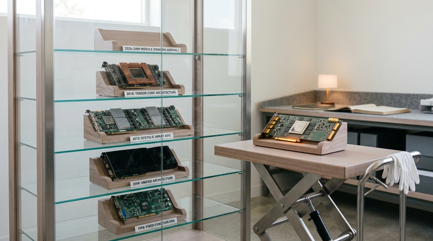
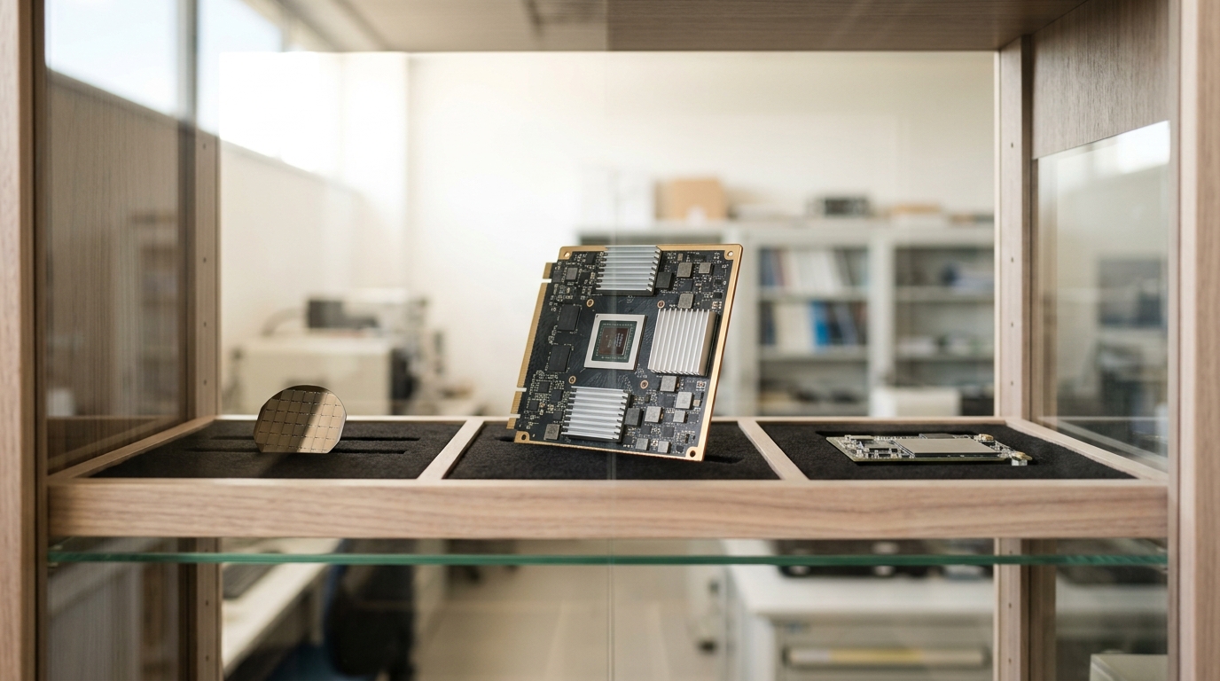
A specimen cabinet holding one board from each era makes a claim a single product announcement never can: that the current generation is a point on a line, not a beginning. The line runs from researchers disguising physics simulations as rendering jobs to get at floating-point throughput nobody had built for them, through a vendor that formalized general-purpose access to that throughput in November 2006, through a week-long training run on two consumer cards that made the whole approach urgent in 2012, through a packaging platform and a memory standard that matured for reasons unrelated to neural networks, through two companies independently arriving at dedicated matrix hardware in the same year, through three startups betting on three different answers to the same bandwidth constraint, to a current generation whose headline numbers are still, at bottom, about how many bytes can reach an arithmetic unit and how few bits each byte needs to carry.
Read any future accelerator announcement against that line rather than in isolation. Ask which part of the recurring constraint — density, bandwidth, distance or precision — the new part is claimed to move, and by how much relative to its own maker’s prior generation, since that is the only comparison the historical record actually supports.