The wafer is a bench, not a product
A processor is not carved out of silicon. It is built up on it, and the distinction matters for everything that follows.
The starting material is a polished disc of monocrystalline silicon, 300 mm across at the leading edge. That diameter has been the state of the art since the early 2000s; a 2016 Congressional Research Service account already described 300 mm as the size that allows maximum production efficiency and noted that moving from 200 mm to 300 mm increases the number of chips per wafer by a factor of 2.25 [17]. The often-discussed move to 450 mm never happened, because the capital cost of retooling exceeded the geometric saving. The disc is not the product. It is the bench on which several hundred products are made simultaneously, and its flatness, purity and crystal orientation set the floor under everything built on top.
On that bench one loop runs, over and over.
Deposit. A thin film is grown or laid down across the whole wafer — an oxide, a nitride, a metal, a barrier a few atomic layers thick. Nothing about this step is selective; it covers everything.
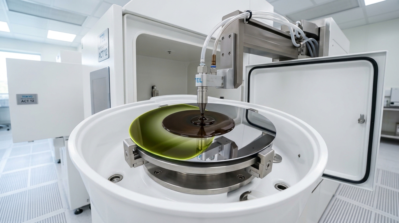
Pattern. A light-sensitive resist is spun on, exposed through a mask to an image of the layer being built, and developed. This is the only step in the loop that carries information. Everything else is bulk chemistry.
Etch. The developed resist protects some regions and not others, and a plasma or a wet chemistry removes material where it is unprotected. The pattern, which existed as a thickness variation in a polymer, becomes a topography in a real material.
Planarise. Chemical mechanical polishing grinds the resulting topography flat again, because the next exposure has a focus budget measured in tens of nanometres and cannot tolerate the hills the previous layer left behind.
Then the loop runs again for the next layer. The same 2016 account put front-end fabrication at more than 250 photographic and chemical processing steps taking about two months [17]; leading-edge flows today involve considerably more, but the shape of the account has not changed. What has changed is that the roadmap now projects the number of critical levels growing faster still, because the industry expects to switch from scaling by shrinking devices to scaling by stacking them [1].
The consequence to hold on to is this: a chip is the residue of a loop, and every pass through the loop is an opportunity to add cost, add variation, and add a defect.
The relation that governs the patterning step
Only one step in the loop carries information, so it deserves the arithmetic. Projection lithography is an imaging problem, and its resolution obeys the Rayleigh relation
where
The relation that is usually left out of popular accounts is the one that costs money:
Depth of focus falls with the square of numerical aperture. Resolution is bought linearly in
There are only three levers, and two of them are nearly exhausted. Wavelength went 436, 365, 248, 193 nm and then stopped. Numerical aperture rose past 1.0 only because immersion lithography put water between the final lens and the wafer, and the refractive index of water caps the useful aperture near 1.35 — a figure ASML calls the highest in the industry for its current 193 nm immersion platform, quoting production resolutions down to 40 nm with quadrupole illumination and 38 nm with dipole [8]. Substitute the vendor’s own numbers back into the relation and the implied

Why extreme ultraviolet, and why the wavelength was not chosen for convenience
The most misunderstood fact about extreme ultraviolet lithography is that 13.5 nm was not selected because it is a convenient wavelength. It is not. The roadmap states the logic plainly: earlier lithography wavelengths were selected where high-intensity narrowband sources existed, whereas the extreme ultraviolet wavelength “is based on the availability of multilayer reflectors with high reflectivity” [1]. The mirror chose the wavelength.
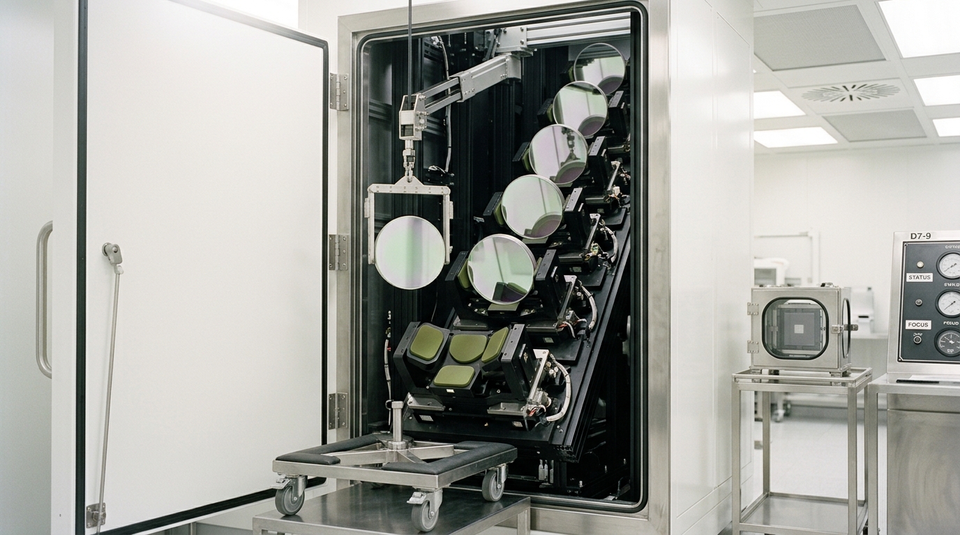
The mirror in question is a stack of alternating molybdenum and silicon layers, each a few nanometres thick, arranged so that weak reflections from many interfaces add in phase. Peer-reviewed work on such coatings reports reflectivity close to 70 per cent at near-normal incidence at 13.5 nm using stacks of around 50 bilayers [14]. ZEISS, which builds the projection optics, claims a coating system delivering up to 70 per cent usable light using up to 100 stacked layers, in a projection module of six mirrors [11]. That is a vendor claim, but it is corroborated in order of magnitude by the independent coating literature.
Now compound it. Six reflections at 70 per cent each pass roughly 12 per cent of the incident light, before anything is lost in the illuminator, at the mask, or in the resist. That single multiplication explains most of the difficulty. It is why source power is the perennial constraint: the roadmap records that 600 W at intermediate focus has been achieved under dose-controlled conditions, with efforts under way to reach 1 kW [1].
The source itself is not a lamp. ASML describes molten tin droplets around 25 microns across, ejected at 70 metres per second, 50,000 times every second; each is struck first by a low-intensity pulse that flattens it into a pancake and then by a far more powerful pulse that vaporises it into a plasma emitting at 13.5 nm [9]. Why tin? Because its plasma emission happens to sit inside the narrow band the mirrors reflect. The peer-reviewed description is that such plasmas are employed as emitters “in a narrow band closely matching the 2% reflection bandwidth centered at 13.5 nm” [13]. Two per cent. Everything outside that window is waste heat.
Three further constraints follow from the wavelength rather than from engineering choices:
Everything is reflective, and everything is in vacuum. ASML states that since most materials absorb extreme ultraviolet light, conventional lenses would simply absorb it [10]. There is no transmissive optic and no air path. The mask itself is a mirror, illuminated off-axis, which introduces shadowing effects with no analogue in transmissive lithography.
The mirrors must be almost impossibly smooth. ASML claims polishing to less than one atom’s thickness, and offers the analogy that if a mirror were the size of Germany its tallest mountain would be one millimetre high [10]. ZEISS offers the same country and puts the figure at 0.1 millimetres [11]. The two vendor analogies differ by a factor of ten, which is a useful reminder that such comparisons are rhetoric rather than specification. The verifiable statement is the one both imply: surface figure and roughness requirements are at the atomic scale.
Masks are the weak point. The roadmap notes that measurement technology for evaluating patterned masks still has many issues, that there are concerns about bright-field masks, sub-resolution assist features and defect control, and that a pellicle with sufficient transmittance and adequate lifetime remains an open issue [1]. A pellicle is the transparent membrane that keeps particles off the mask surface and out of focus; at 13.5 nm, a membrane that is transparent enough and survives the thermal load is genuinely hard. Meanwhile the shift to curvilinear masks and inverse lithography has the potential to multiply mask data volumes more than tenfold [1].
And then there is the photon budget. A 13.5 nm photon carries far more energy than a 193 nm one, so a given exposure dose is delivered by far fewer photons, and the relative shot noise in any small feature rises accordingly. This is not an implementation defect; it is counting statistics. The roadmap projected that dose-to-print would have to rise about threefold over four nodes to hold critical-dimension uniformity against stochastic effects, and reports that the prediction is on track [1]. Higher dose means lower throughput, which means more scanners, which means more capital per wafer. Stochastic control and productivity are the same trade.
It is worth marking what the research frontier does and does not show. Interference lithography at 13.5 nm has demonstrated 5 nm half-pitch patterning in a hydrogen silsesquioxane resist [15]. That is a real result about resist capability, and it is not a statement about scanners: interference tools print periodic gratings, not arbitrary circuit layouts, and carry none of the mask, overlay or throughput burden of a production exposure.
Multiple patterning, and what it actually costs
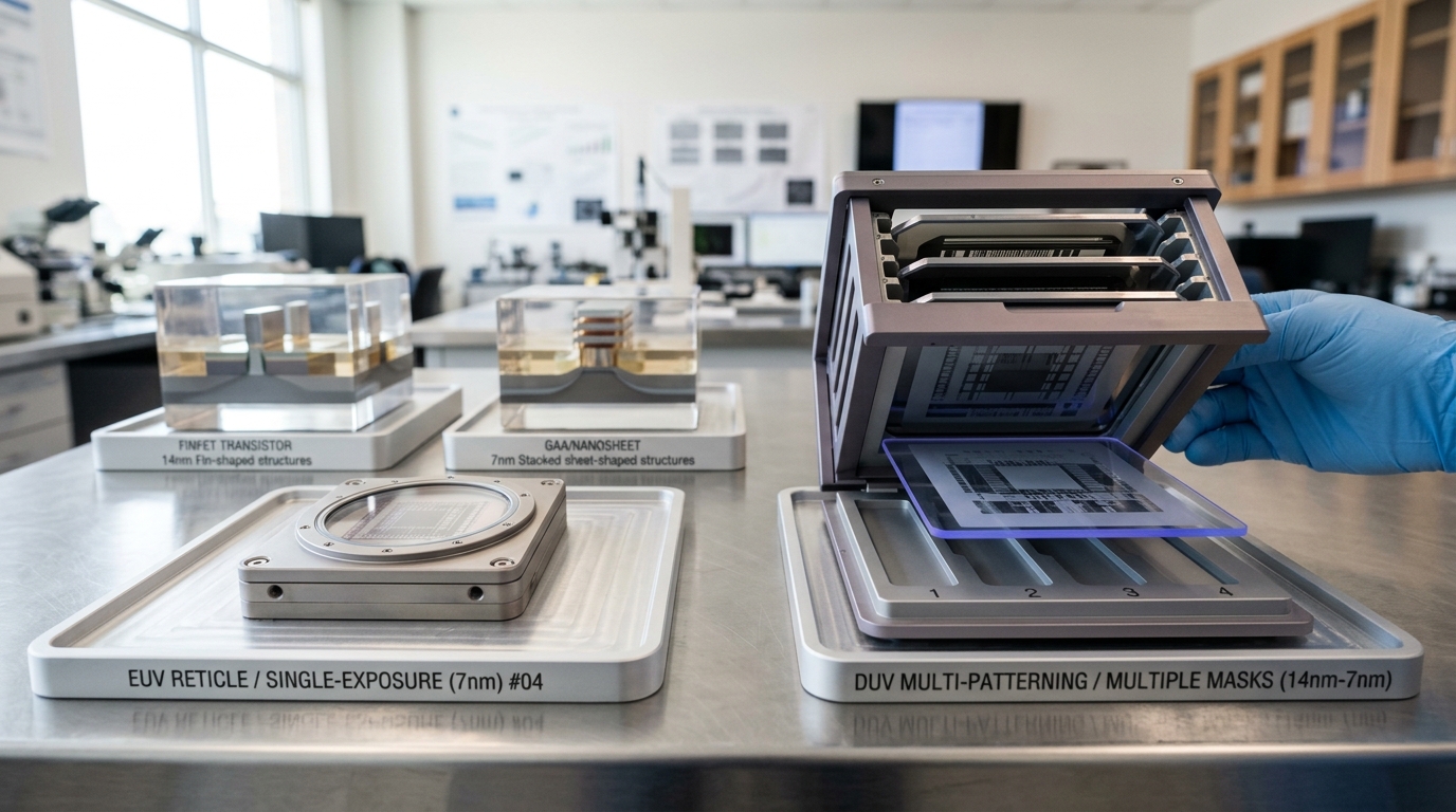
The alternative to a shorter wavelength is to build one dense pattern out of several coarse ones. Litho-etch-litho-etch splits a layout into two or more masks, each individually printable, and interleaves them. Self-aligned double and quadruple patterning instead prints a coarse mandrel, deposits a conformal spacer on its sidewalls, removes the mandrel, and uses the surviving spacers as a mask at half the original pitch — repeating to quarter it.
The cost is not one extra exposure. It is an entire extra circuit of the loop: another deposition, another etch, another clean, another planarisation, another set of measurements. The More Moore roadmap puts the motivation for extreme ultraviolet in exactly those terms — “due to the rising costs and process complexity of multiple patterning, EUV is used as a remedy to pattern-tight ground rules in fewer process steps” [4].
The vendor and research-institute case for higher numerical aperture is built on the same arithmetic. imec assesses that for critical metal layers at its A14 and A10 nodes, 0.33 numerical aperture requires three to four masks where 0.55 accomplishes the layer in a single exposure, and that certain DRAM layers requiring at least three masks today would need one [12]. That is imec’s assessment, not a measured production result, and it should be read as such. ASML’s own product pages state 13 nm resolution for the 0.33 aperture platform and 8 nm for the 0.55 platform [7] — figures that correspond to
Against that, the roadmap is blunt: “It has become clear that EUV will not replace multiple patterning. Both technologies will be used, and the choice of using multiple patterning or not will depend on level-specific details, yield, and cost” [1]. Higher aperture also brings a smaller field. The anamorphic optics needed to keep mask reflection angles manageable use eight-times demagnification in the scan direction and four in the other, halving the maximum wafer field from 26 by 33 mm to 26 by 16.5 mm [1, 6]. Large dies must then be stitched from two exposures, or made smaller and reassembled in the package.
So the honest framing is not “high numerical aperture replaces multiple patterning”. It is that a fab has two currencies for buying pitch — optical aperture and process steps — and spends whichever is cheaper per layer, under a field-size constraint that pushes designs toward smaller dies either way.
Overlay and edge placement error: the constraint that actually binds
Here is the part that popular accounts consistently miss. Printing a small feature and putting it in the right place are different problems, and the second one is now harder.
The roadmap defines edge placement error as the sum of terms covering local variability — line-edge and line-width roughness, local critical-dimension uniformity — and global variability, meaning overlay [1]. It is the quantity that decides whether a via lands on the line it is supposed to contact, whether a cut lands where a cut belongs, and whether two features that must not touch stay apart. Resolution says whether you can print a via. Edge placement error says whether it connects.
If the contributing terms were independent and Gaussian, the budget would combine as
and the largest term would dominate. That independence assumption is exactly what makes the model useful and exactly where it is weakest: overlay and local variability share common causes through the same exposure, the same etch and the same stack. Treat the expression as a budgeting device, not a physical law. The roadmap cites published numerical simulations estimating that overlay takes about 40 per cent of the edge placement error budget and line-edge roughness about 25 per cent [1]. On that split, placement — not printing — is the single largest contributor.
The industry’s structural response is to stop relying on the scanner for placement. Fully self-aligned vias build a multi-coloured material scheme so that etch selectivity, rather than stage positioning, determines where the via lands; self-aligned contact over active gate does the analogous thing at the device level. The roadmap projects increased use of both, precisely because chip area per device is shrinking faster than critical dimensions and the placement budget cannot keep up [1]. This is a genuine change in kind: placement accuracy is being migrated out of the machine and into the materials.
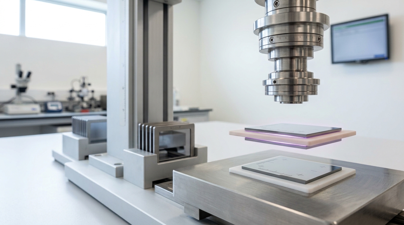
It is worth attaching a number to the scale involved. ASML quotes 2.5 nm cross-matched on-product overlay for its current immersion platform against extreme ultraviolet exposures [8]. That is a vendor specification under vendor conditions rather than a production distribution, but it fixes the order of magnitude: the alignment budget between two layers printed on different machines is a small multiple of a silicon lattice spacing, and it must hold across a 300 mm wafer, across thermal cycles, and across the distortion that every intervening deposition and etch imposes on the wafer itself.
The measurement side is behind. The metrology roadmap states that overlay, “with its continually shrinking budget, remains a constraint in increasing device yield”, and that overlay metrology capability lags the need for improved overlay control, especially for multi-patterning applications [3]. When the measurement is behind the control requirement, the control loop is running partly open.

Variation, defects and the geometry of yield
Every step in the loop has a distribution rather than a value. Some of that variation is systematic and correctable; some is stochastic and is not. On top of it sit discrete defects — a particle, a bridged line, a missing contact.
The particle problem has an uncomfortable structure. The yield roadmap states that the current definition of killer particle size, based on half-pitch, is as small as 3.0 nm for the most critical electrically active particles, and that the critical particle size for manufacture is now below 5 nm — while online monitoring in ultrapure water is limited to laser particle counters capable of 20 nm particles with limited counting efficiency [2]. The particles that kill devices are roughly an order of magnitude smaller than the particles the industry can routinely count. The response documented in the roadmap is to give up on measuring them directly and control the process that produces them instead — a proactive rather than reactive regime [2].
Yield modelling then converts defect density into economics. The widely used negative binomial form is
with
The Poisson limit exposes the die-area relationship in one line. Because the exponent is linear in area, doubling die area squares the yield:
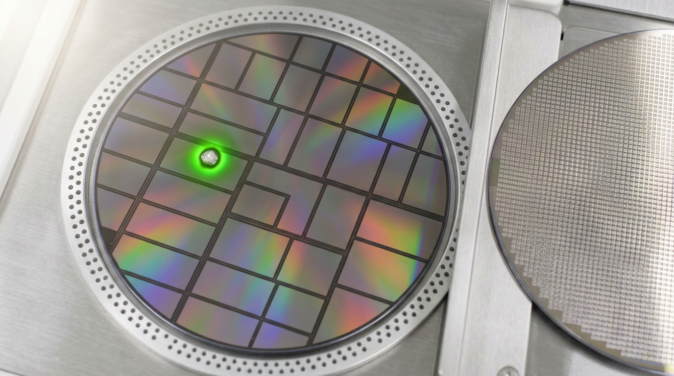
That single exponent is the whole economic argument for disaggregation. It is also why defect-density assumptions deserve scrutiny: the cost model cited above assumes values of 0.13 and 0.12 for its 7 nm and 12 nm cases and explicitly describes them as speculation based on public data [16]. Foundry defect densities are among the least reliably public numbers in the industry, and any cost comparison built on them inherits that uncertainty.
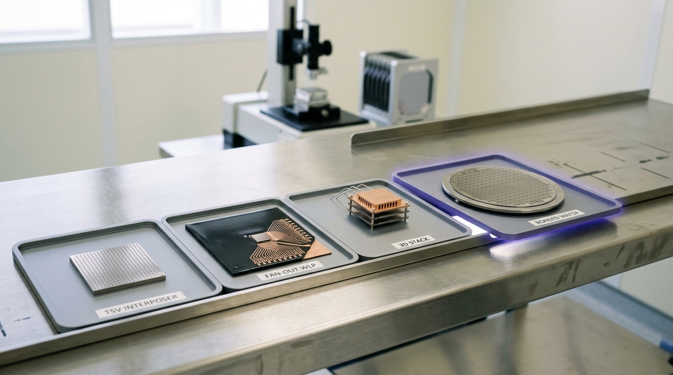
The roadmap draws the conclusion directly. The tradeoff between chip size and yield, combined with the cost of leading-edge logic, means smaller chips plus high-performance packaging may be an alternative to large dies [1]. And the long-term projection is stark: moving to stacked device tiers will require the defect rate per lithographic level to fall by roughly an order of magnitude per node, “instead decreasing 20% or less each node” as it does now [1]. That is not an incremental gap. It is the difference between multiplying the defect rate by about one tenth each node and multiplying it by about four fifths, and the roadmap’s own fallback is explicit: if the required rate is not achieved, dies get smaller and packaging picks up the difference.
Measurement is not overhead; it is the loop
A reader coming from software tends to file metrology under quality assurance. In a fab it is the control system.
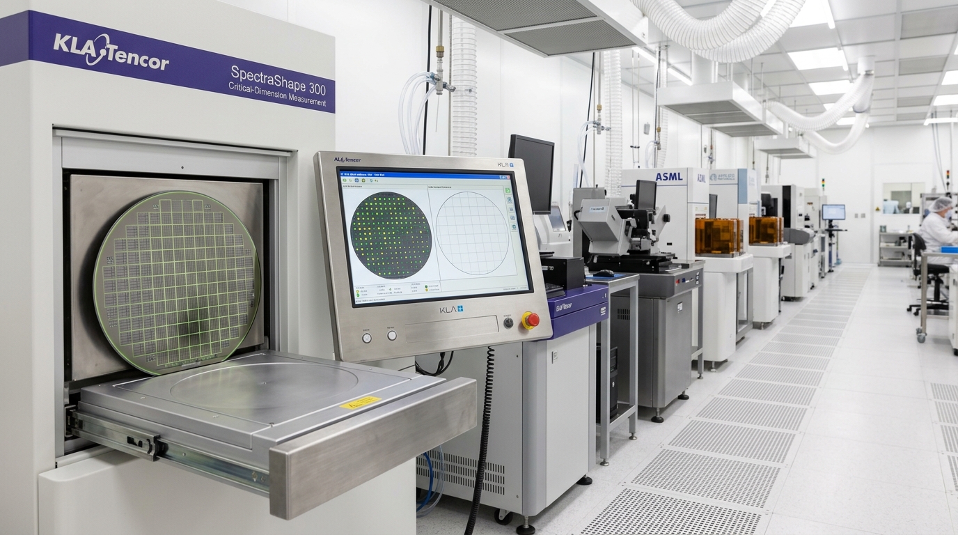
The metrology roadmap describes measurement as enabling process development, control and improvement, tool improvement, pilot-line ramp and factory start-up, and yield improvement in high-volume manufacturing [3]. Nothing in the loop is closed without it: the exposure dose and focus that a scanner applies to wafer number 4,000 are set by measurements taken on earlier wafers.
The instruments are unglamorous and specific. Critical-dimension scanning electron microscopy measures features top-down and suffers from poor depth of field on tall structures. Scatterometry infers line shape by fitting measured optical scatter against simulated libraries, which makes it fast and statistically strong but model-dependent, and the roadmap notes that scatterometry models typically assume uniform optical properties that surface anomalies and non-uniform dopant distributions can violate [3]. Hybrid metrology combines them, using one technique to calibrate another.
Two numbers from the roadmap make the regime concrete. Process monitors report dose errors as low as 1 per cent and focus errors around 10 nm at three standard deviations, and current monitors achieve a precision-to-tolerance ratio of 0.1 across a lithography process window of 15 per cent in dose and 200 nm in focus [3]. Precision-to-tolerance is the quantity that matters: it is measurement variation divided by the tolerance being controlled. At 0.1 the instrument is effectively invisible against the process. As tolerances shrink and the instrument does not improve at the same rate, that ratio climbs — and at some point a meaningful share of what a fab records as process variation is the measurement.
There is a further subtlety worth stating plainly. Dedicated metrology test structures, rather than active devices, are usually what gets measured during manufacturing [3]. What the control loop regulates is therefore a proxy, chosen to be measurable, whose relationship to the electrical behaviour of the actual circuit is itself a modelling assumption. Inspection has the parallel problem: the yield roadmap identifies detecting multiple killer defect types simultaneously, at high capture rate, low cost of ownership and adequate signal-to-noise, as a key challenge [2].
Why the node name tells you nothing
Given all of the above, the label on the process is close to meaningless as a physical description, and has been for roughly three decades.
The dimensional accounting is unambiguous. Transistors made using the so-called 130 nm node actually had 70 nm gates; Intel’s 22 nm FinFET generation contained 26 nm gate lengths, a 40 nm half-pitch and 8 nm fins; and gate length and metal half-pitch, which had tracked one another, diverged in the mid-1990s when gate length began shrinking faster than everything else [5]. After that divergence, no single number could describe a process, and the number that survived was the marketing one.
The roadmap does not pretend otherwise. It states that there is not yet a consensus on node naming across foundries and integrated device manufacturers, and uses its own notation instead: contacted gate pitch, tightest metal pitch, and number of stacked tiers [4]. Two proposed replacements have been circulated in the technical literature — a three-parameter pitch-and-tier scheme, and a triplet of logic, memory and interconnect densities [5]. Neither has displaced the marketing label, and it is worth being clear about why: the label’s function is to signal generation parity with competitors, and a physically honest metric would not serve that function.
The physical dimensions themselves are converging on floors. The roadmap projects physical channel length saturating around 12 nm because electrostatics worsen below that, with roughly 14 nm of width reserved for the device contact [4]. At a node marketed with a label near 2 nm, the smallest structural dimensions remain an order of magnitude larger than the name.
The practical rule is simple. A node name is a product-generation identifier, comparable within one manufacturer’s sequence and not across manufacturers. If a claim depends on a node name, ask for pitches, cell height, tier count, or a density figure with a stated definition; if none is offered, treat the comparison as unsupported.
Predictions, with the observations that would falsify them
These are forecasts, separated from the sourced analysis above. Horizon: 9 August 2029. Assumptions: no lithographic modality outside projection optics reaches high-volume manufacturing within the window, and the current cost relationship between advanced packaging and monolithic scaling does not invert.
One. Edge placement error, not resolution, remains the binding constraint on logic density. Indicator: the majority of publicly described density gains at new nodes are attributed to self-alignment, design-technology co-optimisation and backside power rather than to optical improvement. Disconfirmed if a leading node’s density gain is credibly attributed chiefly to a resolution improvement with placement budgets essentially unchanged.
Two. Higher numerical aperture will reduce but not eliminate multiple patterning at leading logic nodes. Disconfirmed if a foundry publicly ships a leading logic node on which all critical metal levels are single-exposure.
Three. Metrology and inspection will grow as a share of both capital and cycle time, driven by stochastic control and by placement budgets tightening faster than instruments improve. Disconfirmed if published equipment-spending breakdowns show process-control share flat or falling across the window.
Four. Defect-density improvement will not reach the order-of-magnitude-per-node rate that device stacking requires, and disaggregation into smaller dies will continue to absorb the shortfall. Disconfirmed if a manufacturer publishes per-level defect data demonstrating that rate of improvement.
Five. Node naming will not be reformed. Density-based metrics will gain further ground in technical venues while marketing labels continue to diverge from physical dimensions. Disconfirmed if two or more leading manufacturers adopt a shared, physically defined naming convention.
None of these requires a discontinuity. They follow from the structure already documented: a loop whose cost scales with the number of passes, a placement budget that shrinks faster than the tools that measure it, and a yield function that is exponential in area.
What to take away
A chip is a stack of printed layers, and the printing step is the only one that carries information. The physics of that step is governed by a relation in which resolution is bought linearly in aperture and paid for quadratically in focus. Extreme ultraviolet exists because the previous wavelength ran out, and its specific wavelength was chosen by the reflectivity of a molybdenum-silicon stack rather than by anything convenient about the light. Its difficulty — source power, all-reflective optics in vacuum, mask defectivity, photon shot noise — follows from that choice rather than from poor engineering.
But resolution stopped being the frontier some time ago. What limits density now is whether a feature lands where it must, whether the distributions around every step stay inside a shrinking budget, whether the defect that kills the die can be seen at all, and whether the instrument measuring any of it is quiet enough to be trusted. Those are placement, variation, inspection and metrology problems, and none of them is captured by the number in the node’s name — which has not described a physical dimension since the mid-1990s and was never meant to.