A wafer moving through an advanced logic fab passes through something on the order of a thousand process steps, and at the leading edge — the nodes TSMC, Intel, and Samsung call N2, 18A, and SF2 — a meaningful fraction of those steps are now operating close enough to a physical limit that “working” is not a fixed property of the tool. It is a probability that shifts with a handful of tunable parameters the process team adjusts run to run. Understanding advanced fabrication in practice means understanding those loops: what is measured, what is fed back, and where the limit actually sits. This piece works through four of them — exposure and dose control in EUV lithography, the gate-all-around transistor that has replaced the FinFET, the in-line metrology that turns a fab into a control system rather than a sequence of stations, and the yield and capital economics that decide, before a single wafer is exposed, whether a given node gets built at all and where.
Exposure: what “printing a line” costs in photons
Extreme ultraviolet lithography exposes photoresist with 13.5-nanometer light, and the practical consequence practitioners deal with daily is that at this wavelength and at the feature sizes an advanced node requires, the resist is not exposed by a smooth wash of light — it is exposed by a countable number of photons landing in a countable number of resist molecules. Below a few hundred photons per feature, statistical fluctuation in exactly how many photons land, and where, becomes a non-negligible fraction of the signal. That is the physical origin of what the industry calls stochastic defects: not a mask error or a contamination event, but a probability distribution around every single feature that determines whether it prints correctly, prints as a bridge between two features that should be separate, or fails to print (a missing via) [1].
Frederick Chen’s analysis of a real 3-nanometer via layer measured this directly: at typical exposure conditions (roughly 60–89 mJ/cm² depending on resist chemistry), the observed missing-via rate came in at the parts-per-million level — “many orders of magnitude higher than expected from basic estimates” that treat each pixel’s exposure as statistically independent [3]. The gap between the naive estimate and the measured rate is explained by correlation between neighboring exposed pixels: a defect does not need every pixel in a feature to fail independently, it needs a contiguous cluster of neighboring pixels to under- or over-expose together, which happens far more often than independent-pixel statistics predict [3]. The practical lesson for a process engineer is blunt: doubling the dose does not buy proportional improvement. Raising exposure dose reduces the variance of the delivered dose roughly as the square root of photon count, so doubling dose only shrinks statistical spread to about 70% of its previous value — and doubling dose is expensive in throughput, in resist heating and outgassing, and in optics contamination, so the achievable stochastic-defect floor at a given throughput target is a genuine economic trade, not a solved problem.
This is why in-line dose control is treated as a first-class process loop rather than a machine setting checked once at installation: the scanner’s dose sensors and the fab’s CD (critical dimension) metrology are in continuous conversation, adjusting exposure energy lot to lot to hold the delivered dose inside a tight band around the target the resist chemistry was qualified at.
High-NA EUV — the next step up in numerical aperture, from 0.33 to 0.55 — sharpens resolution but introduces its own practical complication. ASML and Zeiss’s anamorphic optics solution for 0.55 NA demagnifies 4× in one direction and 8× in the other, and the resulting “High NA field” covers only about half the wafer area of a standard field [1]. A die that needs the full previous field size now has to be stitched — exposed in two adjacent High-NA fields whose boundary has to align to within a fraction of the smallest feature being printed. A first experimental study of stitching at 0.55 NA, presented at SPIE’s 2025 Advanced Lithography and Patterning conference, treated this as an open patterning problem requiring coordinated solutions across mask design, optical proximity correction, and scanner alignment rather than a solved mechanical tolerance [2]. Imec’s own assessment is that the ecosystem — resist, underlayers, photomasks, and metrology together — only reached a state it was willing to call “ready” in mid-2024, with high-volume manufacturing insertion expected in the 2025–2026 window [1]. That is an industry-consortium assessment of readiness, not a manufacturer’s shipping commitment, and the two should not be read as interchangeable.
The transistor itself: gate-all-around as a manufacturing decision
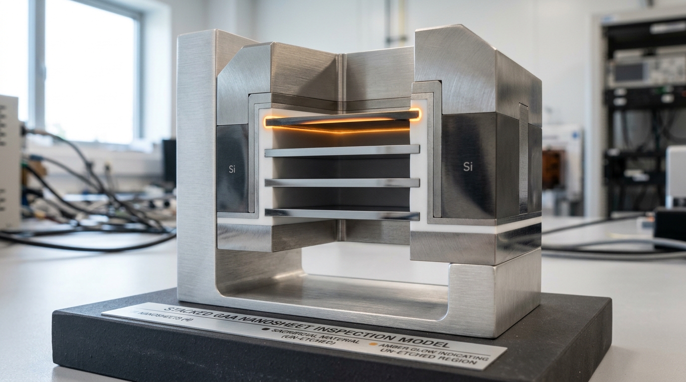
The FinFET, the workhorse logic transistor structure since roughly the 22-nanometer generation, wraps a gate around three sides of a raised silicon fin. At 2 nanometers and below, three-sided control is no longer enough to suppress leakage as the channel shrinks, which is why TSMC’s N2, Intel’s 18A (RibbonFET), and Samsung’s equivalent processes have all moved to gate-all-around nanosheet transistors, where the gate wraps completely around several stacked, released sheets of silicon that serve as the channel [5]. Making that structure is itself a process-control problem: a superlattice of alternating silicon and silicon-germanium layers is grown first, then the sacrificial silicon-germanium is selectively etched out between the silicon sheets to release them, leaving free-standing nanosheets that the gate stack is deposited around. Etch selectivity, sheet-to-sheet thickness uniformity, and how cleanly the sacrificial material is removed without damaging the released sheets are all now yield-limiting variables in their own right, distinct from anything the lithography step controls.
TSMC’s N2 disclosure at IEDM 2024 — presented by VP of R&D Geoffrey Yeap — reported 10–15% speed gain at equal power, or roughly 25–35% power reduction at equal speed, relative to the company’s N3 process, alongside a claimed 15% or better density improvement and an SRAM macro density of about 38 megabits per square millimeter, described as a record [4] [6]. These are TSMC’s own reported figures from its IEDM presentation, not independently reproduced third-party measurements, and they should be read as a manufacturer disclosure rather than an audited result. Intel’s parallel IEDM material covered scaling of its RibbonFET nanosheet transistors for its 18A generation [5]. Comparing the two companies’ percentage claims directly is not sound practice: they are measured against each company’s own prior node under each company’s own test conditions, and neither figure is a third-party benchmark against a common reference — a point worth stating plainly rather than building a ranking that the underlying numbers cannot support.
Metrology: the loop that makes a fab a control system, not an assembly line
None of the above works as a description of “what a fab does” without the layer that sits between every pair of process steps: in-line metrology. After a litho exposure, before the wafer moves on to etch, an overlay metrology station measures how precisely the newly printed pattern is aligned to the layer already on the wafer, typically using a “grating-on-grating” scatterometry target — two overlapping diffraction gratings whose relative offset is read out optically rather than imaged directly, because optical scatterometry can resolve sub-nanometer offsets faster than electron microscopy can. Critical-dimension SEM measurements sample actual feature widths at selected sites. Both measurements feed back into the exposure tool’s alignment model for the next wafer in the lot, and into longer-run statistical process control charts that flag drift before it produces visible defects. This is the sense in which an advanced fab is a control system: the output of one station is the input to the correction applied at an earlier station on the next unit, on a cycle measured in minutes, not the batch-review cycle of a conventional manufacturing line.
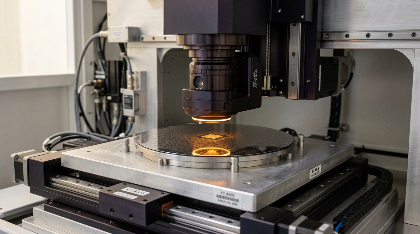
The stakes of getting this loop wrong compound with node complexity. Multi-patterning — splitting one design layer into two or more separate exposures because a single EUV or DUV exposure cannot resolve the pitch — makes overlay between the sub-exposures part of the effective critical-dimension budget: an overlay error between mask A and mask B of a split layer behaves, electrically, exactly like a critical-dimension error within a single exposure. That is one of the concrete reasons EUV’s single-exposure capability at tighter pitches was pursued in the first place — not only resolution, but removing an entire category of overlay error that multi-patterning introduces.
Yield: pricing a wafer before it is finished
A finished, fully-processed 300-millimeter wafer at an advanced node carries somewhere in the
neighborhood of several hundred to a few thousand individual dies, and not all of them will work.
The simplest model process engineers reach for treats random defects as a Poisson process across
the wafer: given an average defect density
This Poisson form is known to be pessimistic in practice, because real defects cluster rather than
distributing independently across the wafer — a particle-contamination event or a localized etch
non-uniformity produces several nearby failures at once, not one failure drawn independently from a
uniform background. Models that account for clustering (the negative binomial family, of which
Murphy’s model is a well-known special case) generally predict a higher yield than the naive Poisson
formula for the same nominal defect density, because clustering means large stretches of the wafer
are defect-free even at a defect density that would look damaging if it were spread evenly. Which
model actually fits a given fab’s data is an empirical question the fab’s yield-management team
answers continuously, not a constant chosen once —

Testing closes the loop from a manufacturing perspective: wafer-sort probing every finished die before dicing, checking for the specific failures the process is known to produce, converts the yield model’s population-level prediction into a per-die pass/fail result that determines what fraction of a wafer’s cost is actually recovered in sellable parts. A wafer that costs on the order of $28,000–30,000 to process at the 2-nanometer node, by one industry cost-modeling firm’s estimate — up roughly 50% from 3-nanometer wafer costs by the same estimate — makes the yield percentage a direct multiplier on the economics of every design that uses that node [7]. That $28,000–30,000 figure is a third-party cost-modeling estimate (International Business Strategies, as reported by Tom’s Hardware), not a disclosed price from any foundry, and foundries do not publish their actual internal wafer costs.
Fab economics: why the leading edge concentrates where it does
The same cost-modeling estimate put the capital cost of building a single 2-nanometer-capable fab, sized around 50,000 wafer starts per month, at roughly 28 billion US dollars — a number that sits inside a broader industry capex picture reported at around 200 billion US dollars for 2026 across the whole sector, a roughly 20% increase over 2025’s 166 billion, with TSMC alone projecting 2026 capex of 52 to 56 billion dollars, up 27–37% from the 40.9 billion it spent in 2025 [7] [9]. That scale of committed capital, recovered only over a multi-year production run and only if the process reaches competitive yield quickly, is the underlying reason advanced-node capacity concentrates in a small number of companies and a small number of sites rather than spreading the way commodity manufacturing does: the fixed cost of entry is now large enough that only a handful of firms can make the bet at all, and each of those firms concentrates its own most advanced capacity in the locations where it has already paid down the learning curve.

That concentration is now being tested directly by geographic diversification. TSMC’s Arizona site began high-volume production on N4 process technology in late 2024, and Rick Cassidy, president of TSMC’s US subsidiary, stated that the Phoenix fab’s yield ran about four percentage points higher than comparable Taiwan fabs running the same process — attributed, in the reporting, to lessons carried over from the mature Taiwan process rather than to anything specific about the Arizona site [8]. That is a single manufacturer’s public statement about one node at one site, reported by one outlet citing Bloomberg — a useful data point against the assumption that offshore fabs necessarily under-perform their origin site on yield, but not a general finding about geographic diversification, and it says nothing about cost, which industry reporting elsewhere describes as running 30–50% higher for the first offshore fab due to labor, regulatory compliance, and the one-time cost of standing up a new site’s supply chain. Yield and cost are separate questions, and a good yield result at Arizona does not by itself resolve the cost question.
What advanced disagreements look like in this field
It is worth being explicit about where practitioners genuinely disagree, rather than presenting advanced fabrication as a solved engineering discipline that simply awaits execution. The choice of yield model is one real disagreement: some fabs’ statistical process control groups treat the negative binomial family as the default and calibrate its clustering parameter continuously against in-line inspection data, while others still use simpler Poisson-based estimates for early-stage capacity planning precisely because the negative binomial model needs more historical defect data than a brand-new node has yet produced. Neither camp is wrong so much as answering a different question — a capacity planner needs a defensible number on day one of a new node, while a yield engineer six months into production has the inspection history to justify a more accurate model.
A second live disagreement concerns how much of the stochastic-defect problem EUV dose control can actually absorb versus how much has to be solved in the resist chemistry itself. Chen’s analysis of pixel-clustering effects argues that a meaningful share of the excess defectivity above naive photon-shot-noise estimates comes from correlated neighboring-pixel behavior in the resist’s chemical response, not from the exposure tool’s dose delivery [3]. If that is the dominant mechanism, then further improvements in scanner dose stability have a lower ceiling than improvements in resist material design — a claim that assigns responsibility to a different part of the supply chain than a purely optics-centric account would, and one this article treats as a specific researcher’s analysis rather than settled consensus, since resist vendors and scanner vendors have an obvious incentive to prefer one framing over the other.
Reading a fab’s own disclosures with the right skepticism
A practitioner-level account of fabrication also has to say something about how to read the industry’s own claims, because IEDM and manufacturer disclosures are not neutral data releases — they are timed, curated statements meant to support a specific competitive narrative, typically ahead of a customer commitment cycle. TSMC’s N2 percentage improvements, Intel’s RibbonFET scaling claims, and Samsung’s parallel disclosures are all measured against each company’s own immediately prior node, under each company’s own test conditions and workload mix, and none of the three companies discloses the raw defect-density or yield data that would let an outside party check the claim independently. That is not evidence the numbers are false; it is a structural reason to treat a “15% faster, 30% lower power” headline as a manufacturer’s characterization of its own internal comparison rather than as a third-party benchmark result, and to avoid constructing a cross-company ranking from figures that were never measured on a common basis in the first place. The same caution applies to cost figures: the widely cited $28,000–30,000-per-wafer estimate for 2-nanometer processing comes from an outside consulting firm’s cost model, not from a foundry’s own disclosed pricing, and consulting-firm cost models are built from public capital-spending figures, industry interviews, and modeling assumptions that are not fully auditable from outside [7].
What this means going forward
Two forward-looking claims are worth stating with their conditions attached, since the discipline this article has tried to hold is separating what is known from what is projected.
Scenario, not prediction: if High-NA EUV insertion proceeds on the 2025–2026 timeline imec described, stitching will move from an experimental patterning problem to a standard design constraint that IC layout tools handle automatically — the way multi-patterning-aware layout became routine a decade earlier. The observable indicator to watch is whether EDA vendors ship stitching- aware place-and-route as a default flow rather than a special case; if High-NA insertion instead slips past 2027 without that tooling shift, treat the scenario as not materializing.
Prediction, five-year horizon: capital cost per leading-edge fab will keep rising faster than overall semiconductor capex, concentrating new leading-edge capacity in fewer than five companies worldwide by 2031. The assumption underneath this is that stochastic-defect and metrology overhead continue to rise with each node rather than plateau. The disconfirming observation would be a new entrant successfully bringing up a leading-edge (sub-2-nanometer-class) fab to competitive yield within its first three years of operation — Musk’s announced Terrafab project, at a reported 20–25 billion dollar cost, is the nearest live test of exactly this claim, and its outcome by roughly 2029 would settle the question either way [9].
None of this is exotic engineering in the sense of being unprecedented — every step described above has been disclosed in some form at IEDM or SPIE, or by a manufacturer directly. What makes advanced fabrication difficult in practice is that dozens of these loops run simultaneously, each one operating close enough to a physical or economic limit that small drifts compound, and the fab’s entire job is holding all of them inside their control bands at once, lot after lot, for years.