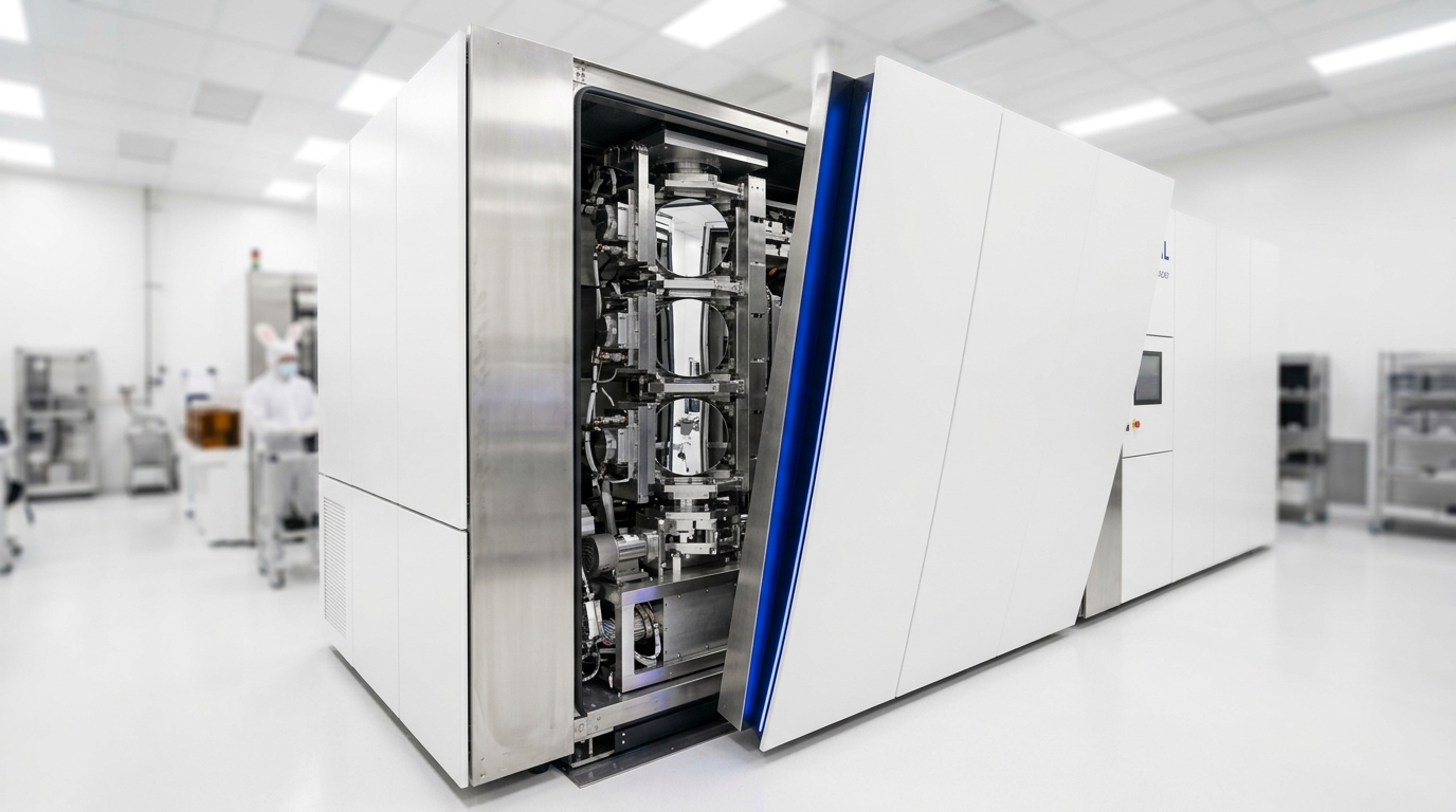
The step that checks all the other steps
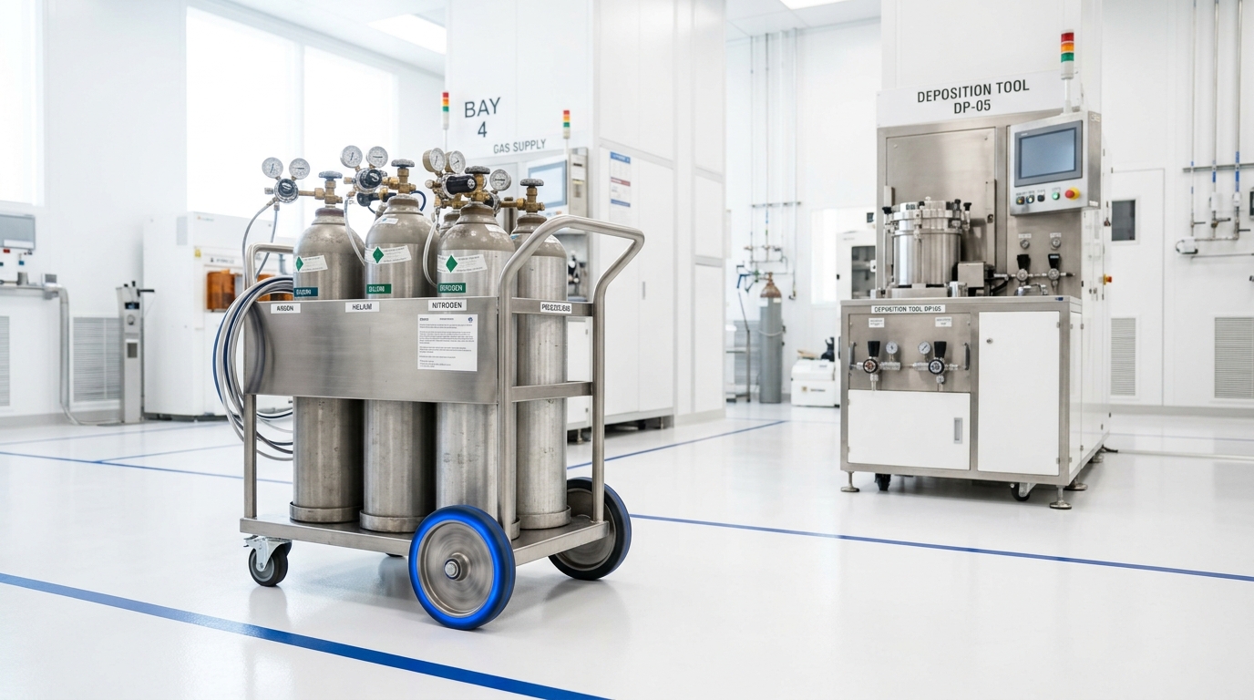
Applied Materials builds layers up. Lam Research cuts patterns into them. ASML defines those patterns with light. None of those three companies’ tools can tell a fab whether the result actually worked. That verification job — finding the microscopic defects and measuring the exact dimensions that determine whether a chip functions — is KLA’s specialty, completing the four-company equipment structure this cohort maps: deposition, etch, lithography, and inspection, each led by a different company [1].
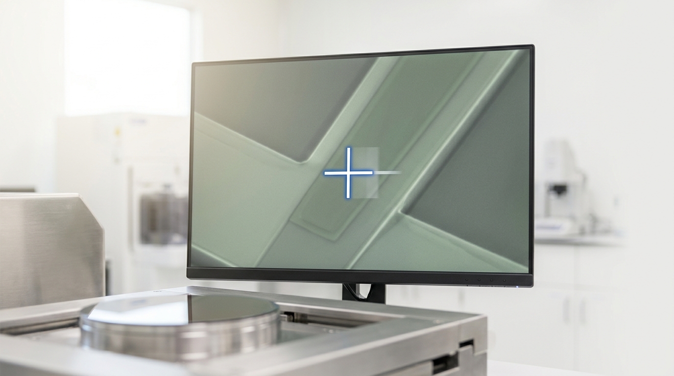
Why inspection has become more consequential, not less
As chip features shrink toward the physical limits this cohort’s other equipment briefings document — sub-2nm transistors, TSVs etched at extreme aspect ratios, EUV-patterned features at the edge of what light can resolve — the defects that matter have shrunk right alongside them. A flaw that would have been irrelevant at an older, larger process node can now be large enough, relative to a modern transistor’s size, to render an entire die non-functional. KLA’s inspection and metrology tools have to keep pace with that shrinking tolerance at every single process generation, making inspection sensitivity itself a genuine, ongoing engineering race parallel to the lithography and etch races covered in this cohort’s other equipment briefings.
The direct connection to this cohort’s yield-economics coverage
This cohort’s SMIC briefing traces a reported 20-40% yield on Huawei’s Ascend 910C directly to manufacturing constraints, and its companion briefing on that yield gap explains why low yield compounds the cost of every working chip that does ship [2]. Inspection and metrology are the direct mechanism by which any fab — SMIC’s or TSMC’s alike — actually measures its own yield in the first place: without KLA-class inspection capability, a fab would not even know precisely which dies are defective and why, let alone have the process-control data needed to improve yield generation over generation. Every yield figure cited anywhere in this cohort was ultimately measured by equipment in this same category.
Why inspection sits closer to the customer relationship than the other three
Unlike deposition, etch, and lithography, which each perform one well-defined physical transformation on the wafer, inspection and metrology data feeds directly back into a fab’s own process-control decisions in real time — informing which process steps need adjustment, which tools need recalibration, and ultimately which dies are worth continuing to process through the remainder of an expensive, many-step manufacturing sequence. That tight feedback loop makes KLA’s relationship with its fab customers unusually data-intensive compared to the other three equipment categories, and it is part of why the overall semiconductor capital equipment market, inspection included, continues to grow alongside the capacity expansions covered throughout this cohort’s foundry track [3].
The unglamorous truth about who actually enables Moore’s Law
Popular accounts of the semiconductor industry’s continued progress tend to credit lithography — smaller wavelengths, higher numerical apertures — as the whole story. KLA’s role is a necessary corrective to that framing: none of the industry’s continued scaling would be commercially viable without the inspection and metrology capability to actually verify, at every process generation, that the increasingly difficult manufacturing steps genuinely worked. Progress that cannot be measured cannot be trusted, and trust, at this level of manufacturing precision, is KLA’s actual product.
Why advanced packaging raises the stakes for inspection specifically
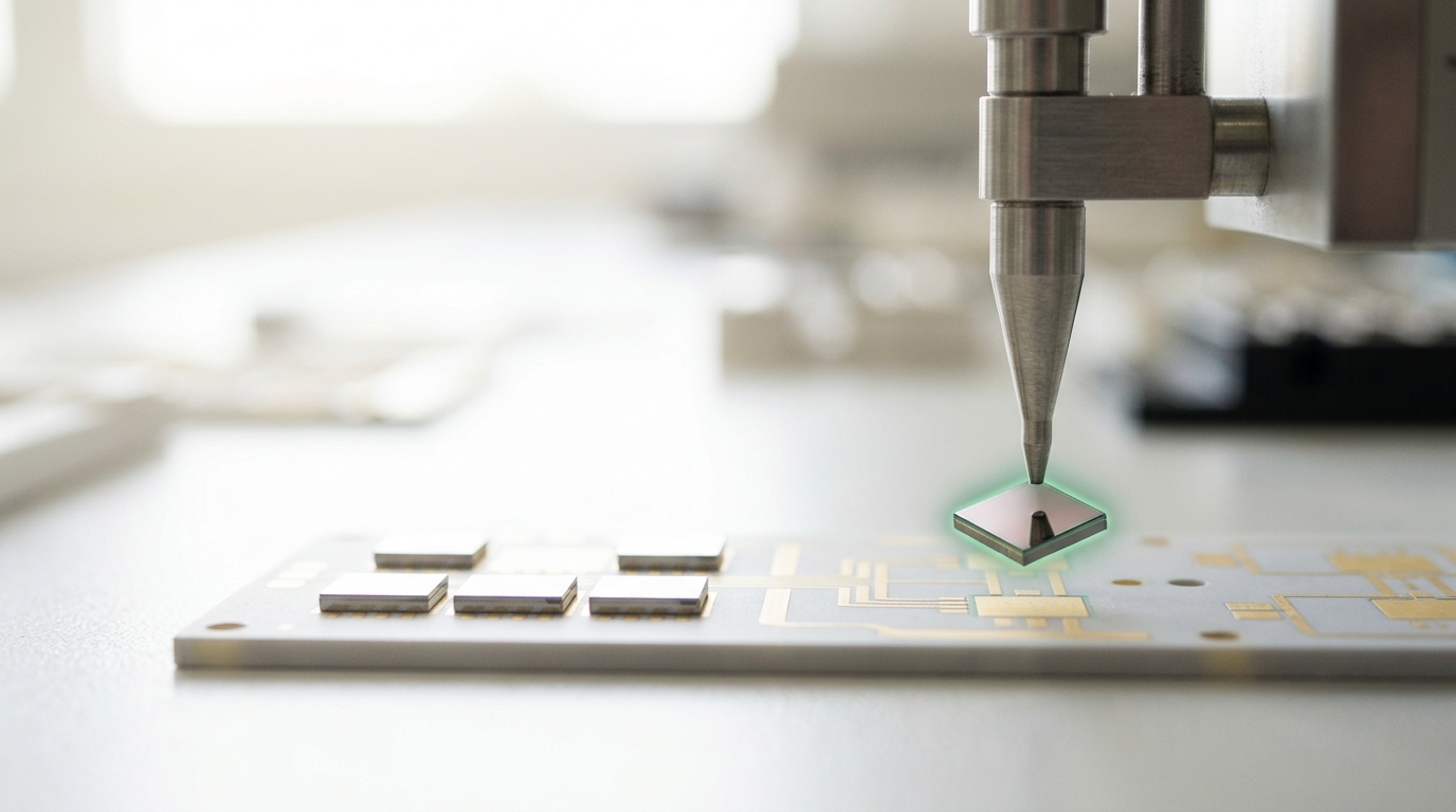
This cohort’s TSMC CoWoS briefing documents advanced packaging as the binding 2026 constraint on AI accelerator supply, ahead of wafer capacity itself [4]. Packaging introduces entirely new categories of defects inspection has to catch — misaligned interposer bonds, voids in thermal interface layers, warpage across a multi-die substrate — none of which existed as inspection targets in the era of simpler, single-die packages. KLA’s inspection and metrology scope has had to expand into this packaging domain alongside the industry’s broader shift toward chiplets and heterogeneous integration, making the company’s relevance grow in step with exactly the packaging bottleneck this cohort documents as 2026’s defining supply constraint.
Why a reader should track KLA’s own capex guidance
Because inspection tools have to be qualified and installed alongside every new deposition, etch, and lithography tool a fab adds, KLA’s own equipment shipment and bookings data offers a useful cross-check against the capacity-expansion announcements covered throughout this cohort’s foundry track: a fab that is genuinely ramping new capacity needs proportional new inspection capacity too, and a mismatch between the two would be an early signal worth investigating.