The layer before the pattern
ASML’s lithography machines pattern a chip’s features. Before that patterning can happen, the material those features are carved into has to exist on the wafer in the first place — and building up that material, one atomic layer at a time, is Applied Materials’ specialty within the four-company equipment structure this cohort maps: AMAT leads deposition, Lam Research leads etch, KLA leads inspection, and Tokyo Electron leads thermal processing, each a genuinely distinct business despite frequently being grouped together loosely as “equipment stocks” [1].

What deposition actually is
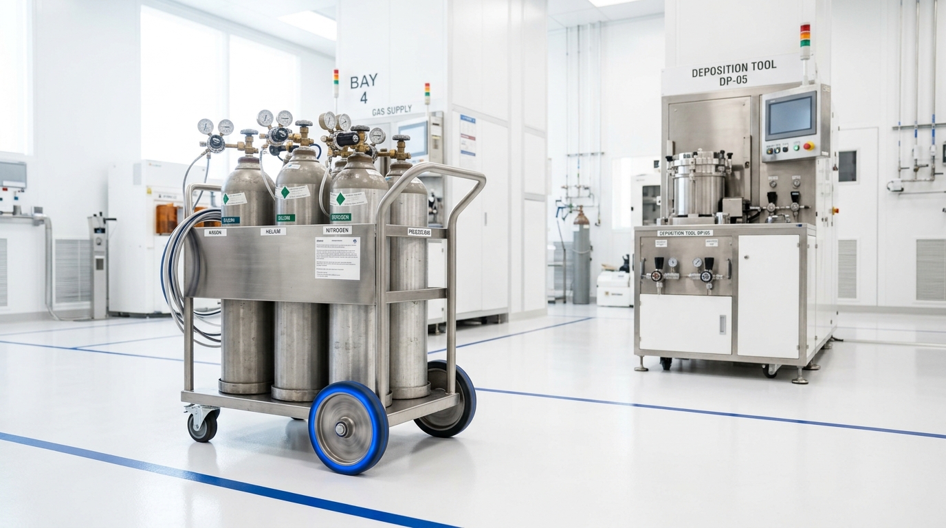
Deposition is the process of building a thin, precisely controlled film of material — a conductor, an insulator, a semiconductor layer — onto a wafer’s surface, typically by introducing a carefully metered gas that reacts or condenses into a solid film atom by atom. Every transistor, every interconnect layer, every one of the dozens of distinct material layers that make up a modern chip has to be deposited by a tool broadly in this category before it can be patterned, etched, or otherwise processed further. A leading-edge logic chip can require dozens of separate deposition steps across its full manufacturing process, each one demanding precise thickness and composition control.
Why this segment scales differently than lithography
Unlike ASML’s EUV monopoly, deposition equipment has multiple credible suppliers globally, though Applied Materials holds the leading position specifically in the segment overall. That structural difference matters: deposition problems are, in a meaningful sense, more numerous and more varied than the single hardest problem lithography solves, since different material layers on a chip call for different deposition techniques and chemistries, creating room for more than one company to develop genuine expertise across different sub-segments of the same broader category, rather than the winner-take-all dynamic EUV lithography produced.
How AMAT’s business connects to the rest of this cohort’s foundry coverage
Every fab expansion covered in this cohort’s foundry track — TSMC’s N2 ramp, Intel’s 18A/14A buildout, Samsung’s 2nm push — represents new deposition equipment capacity that has to be installed and qualified alongside the lithography tools that get most of the attention. Deposition capacity additions typically track wafer-fab capacity additions closely, since every new fab needs both in roughly matched proportion, which is why the semiconductor capital equipment market as a whole, including deposition specifically, is projected to keep growing alongside the leading-edge capacity expansions this cohort documents extensively elsewhere [2] [3].
Why this unglamorous layer deserves more attention than it gets
Deposition rarely generates headlines the way a new lithography node or a blockbuster accelerator chip does, but a defect or inconsistency introduced at the deposition stage propagates through every subsequent manufacturing step, potentially ruining a chip that would otherwise have passed through a perfectly executed lithography and etch process. Applied Materials’ business is, in this sense, foundational rather than glamorous — exactly the kind of essential, unglamorous layer this cohort’s equipment-and-materials track exists to surface for readers who otherwise only encounter the more visible layers of the chip supply chain.
The scale this business operates at
Deposition equipment sits inside a global semiconductor market projected at roughly $1.3 trillion in 2026, per Gartner’s estimate cited throughout this cohort’s market-overview research [4]. Applied Materials’ revenue depends on capturing a durable share of the capital equipment spending that flows from that broader figure, which means the company’s own fortunes track the industry’s overall capex cycle closely — a cyclical business, like most of the equipment layer, rather than one insulated from the swings in fab investment that ripple through every company covered in this cohort’s foundry track when demand shifts.
What distinguishes Applied Materials from a pure commodity supplier
Despite operating in a segment with more competition than ASML’s lithography monopoly, Applied Materials maintains its leading position through accumulated materials-science expertise across an unusually broad range of deposition chemistries and process types, spanning the many different material layers a modern chip requires. That breadth is itself a competitive moat: a newer entrant would need to replicate expertise across dozens of distinct deposition processes simultaneously to compete credibly at Applied Materials’ scale, a much broader technical surface area to match than a narrower, single-process competitor would need to cover.