Five companies, five distinct jobs, one sequence
This cohort has profiled five semiconductor equipment companies individually — enough separate briefings that the relationship between them deserves its own reference piece. Here is the complete sequence, in the order a wafer actually passes through it, with the company that leads each step:
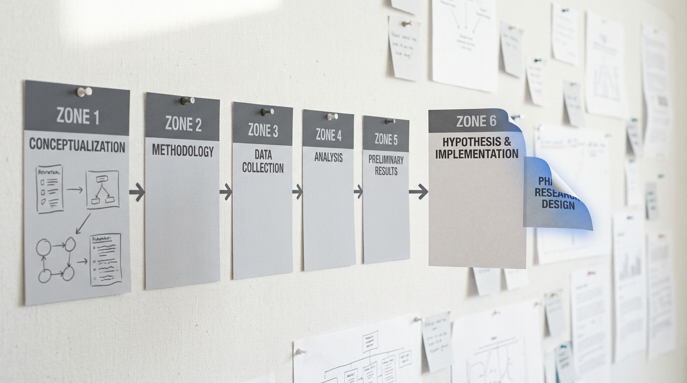
The chart above orders the steps for reference; in practice a real wafer cycles through deposition, coat/develop, lithography, etch, and inspection repeatedly, often dozens of times, as each of a chip’s many layers is built up in turn — not once in a single pass.
The five jobs, in plain terms
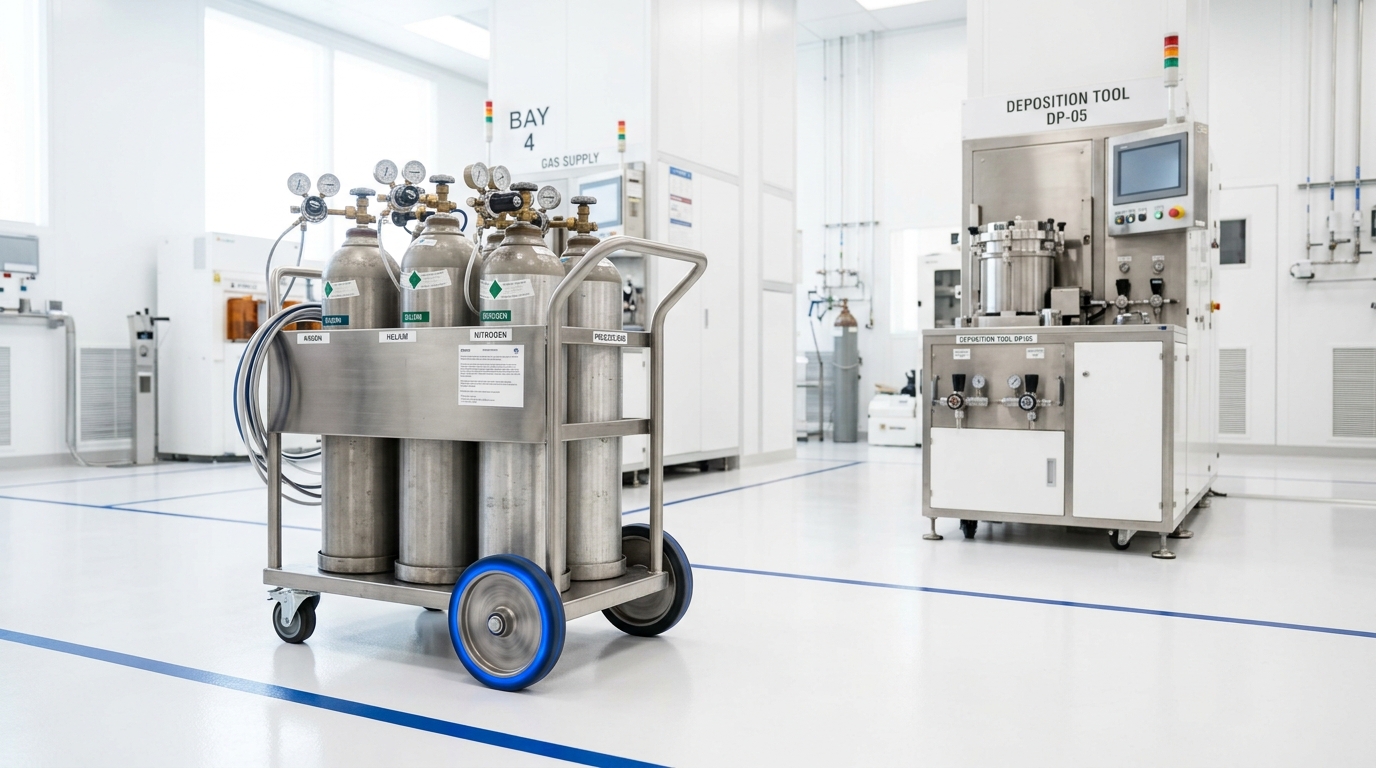
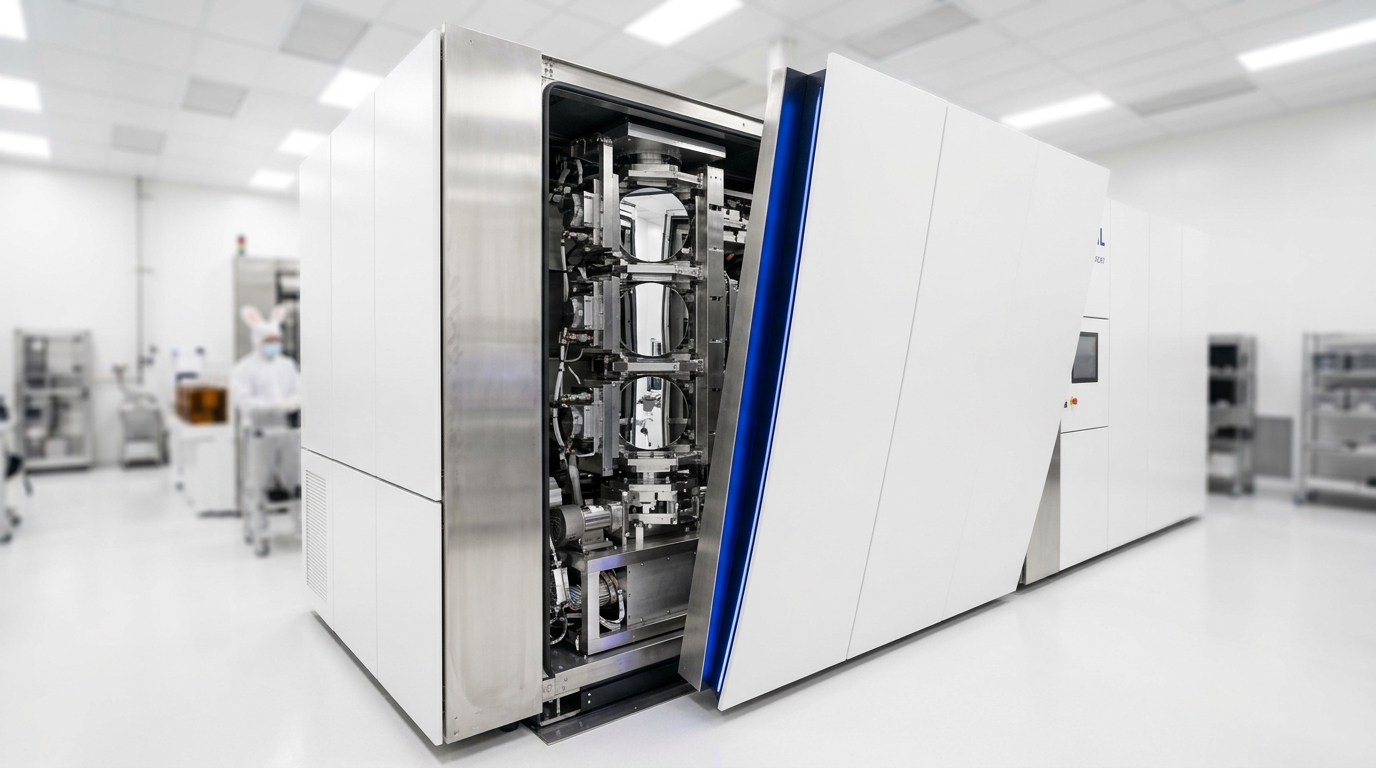
Applied Materials (deposition): builds up the precise atomic layers a chip’s structure is physically made from. ASML (lithography): the sole global source of the light-based patterning that defines where every feature goes — this cohort’s companion briefing establishes why no competitor exists. Lam Research (etch): removes material precisely to turn a patterned layer into an actual physical structure, including the deep TSV etch that makes HBM stacking possible. KLA (inspection and metrology): finds the microscopic defects and measures the exact dimensions that determine whether all of the above actually worked. Tokyo Electron (coat/develop and thermal processing): the connective tissue between every other step — applying and developing resist, managing the thermal budget a wafer experiences throughout the entire sequence [1].
Why no single company can do all five well
Each of these five jobs requires a genuinely different kind of engineering expertise — optics and photonics for lithography, plasma physics for etch, materials chemistry for deposition, precision metrology for inspection, thermal and fluid dynamics for coat/develop. That is the structural reason this segment supports five specialized leaders rather than one dominant equipment conglomerate: the accumulated expertise required in each category is deep enough that a company excelling at one has little natural advantage in the others, unlike some other layers of the chip industry covered elsewhere in this cohort where a single company’s scale advantage compounds across multiple related functions.
The sixth step this chart leaves out
Notably, this five-step sequence ends with a finished, patterned wafer — not a sellable chip. This cohort’s ASE Technology and Amkor briefings cover the packaging and test step that still has to happen afterward, a step increasingly critical enough on its own, per this cohort’s CoWoS briefing, to represent the binding constraint on 2026 AI accelerator supply rather than any of the five wafer-fabrication steps mapped above [3] [4].
How to use this map
Treat this briefing as a reference to return to whenever another article in this cohort mentions one of these five companies or their associated process step without re-explaining it. Together with the equipment market’s broader growth trajectory tracked across this cohort’s research [2], this map is the skeleton the rest of this cohort’s equipment-and- materials coverage hangs on.
Why this layer is easy to overlook and hard to replace
None of these five companies puts its name on a finished product a consumer ever sees. Nvidia’s name is on the GPU; TSMC’s is at least known to readers who follow the industry closely. ASML, Applied Materials, Lam Research, KLA, and Tokyo Electron sit one and two layers further removed from any visible product, which is precisely why this cohort has given each its own dedicated briefing — the layer is easy to overlook in casual coverage and correspondingly hard to replace if any single company in it stumbles, given how specialized and accumulated each company’s expertise actually is.
The through-line across all five companies
Every one of these five companies appears, directly or indirectly, in nearly every other track of this cohort’s hundred-article survey: the foundry track’s fab-capacity announcements assume sufficient equipment from all five; the memory track’s HBM shortage traces partly to Lam Research’s etch capacity; the packaging track depends on tools each of these companies supplies in some form. Understanding this map is, in a real sense, understanding the shared foundation underneath almost everything else this cohort covers.