What “High-NA” actually means
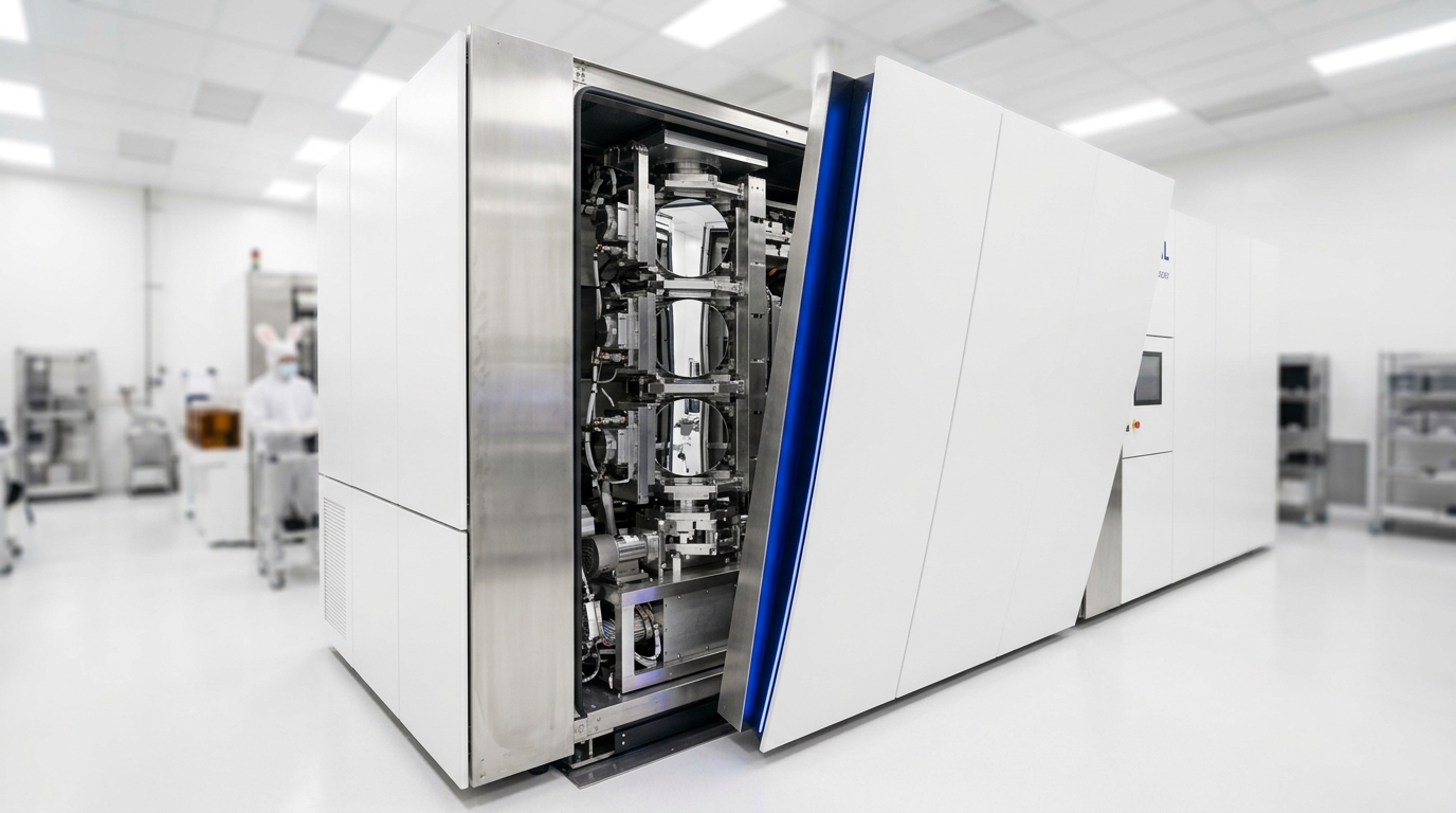
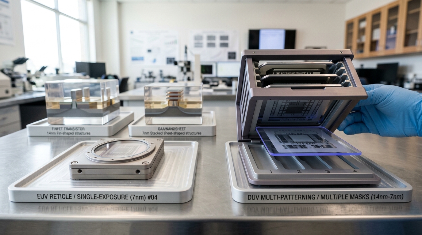
“NA” stands for numerical aperture — a measure of how tightly a lens system can focus light. A higher numerical aperture lets an EUV scanner resolve finer features on a chip in a single exposure, without resorting to the multiple-patterning workarounds this cohort’s SMIC briefing describes Chinese fabs using out of necessity with older DUV tools. ASML’s High-NA platform is the next-generation evolution of EUV itself, launched in 2026 with source power raised toward 1,000 watts, directly increasing the number of wafers the tool can pattern per hour [1].
The production milestones, not just the lab demonstrations
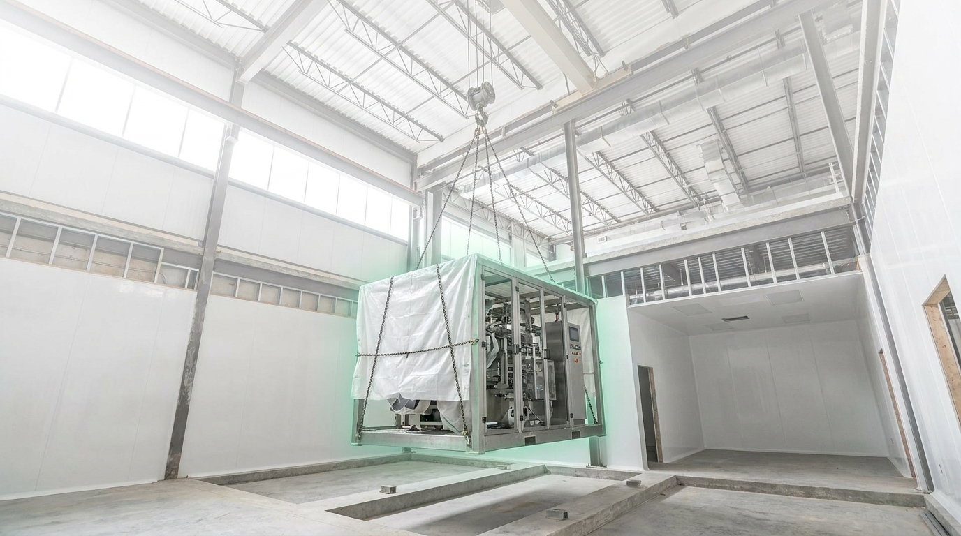
By mid-2026, more than 300,000 wafers had already been processed on High-NA tools at customer sites — a real, running production tally rather than a laboratory proof of concept [1]. In July 2026, High-NA reached a specific readiness milestone: the first high-volume logic product, developed through close technical collaboration between Intel and ASML [2]. Separately, the EXE:5200 High-NA tool has entered customer fabs including first deliveries to SK hynix, positioning High-NA as the primary driver for future advanced DRAM and sub-2nm logic simultaneously [2].
Why this matters more than a routine equipment upgrade
Ordinary EUV lithography, the technology covered in this cohort’s companion ASML briefing, is already reaching its practical resolution limits at the most advanced nodes without resorting to multiple exposures — which adds cost, time, and defect risk, the same trade-off this cohort’s SMIC briefing documents Chinese fabs accepting out of necessity with older tools. High-NA EUV pushes that resolution ceiling higher again, meaning it is the specific technology that determines whether the industry’s node-shrinking roadmap — the same roadmap underlying TSMC’s N2/A16 plans and Intel’s 18A/14A ambitions, both covered elsewhere in this cohort — has a viable path forward for another generation, or hits a wall requiring far more expensive multi-exposure workarounds industry-wide.
Demand context: is the growth durable
ASML reported roughly 30% EUV growth in 2025, and the open question industry analysts were asking heading into 2026 was whether that growth rate was sustainable or a one-time catch-up surge [3]. The subsequent order data — SK hynix’s $8 billion commitment covered in this cohort’s companion briefing, plus the Intel and SK hynix High-NA milestones described above — suggests durable, structural demand rather than a temporary spike, though ASML’s own future quarterly bookings remain the most reliable ongoing evidence to track rather than any single company’s commentary [4].
What to watch through the rest of the decade
The clearest forward indicator is the pace at which High-NA tools move from “first high-volume logic product” milestones, as reached with Intel in July 2026, to broad multi-customer volume production. A rapid broadening of the customer base beyond the initial Intel and SK hynix milestones would confirm High-NA EUV as the industry’s next mainstream lithography platform on schedule; a slower rollout would suggest the transition is proving more difficult than the initial 300,000-wafer milestone implies, with direct consequences for every node-scaling roadmap covered throughout this cohort’s foundry track.
Why High-NA adoption is a coordination problem, not just an engineering one
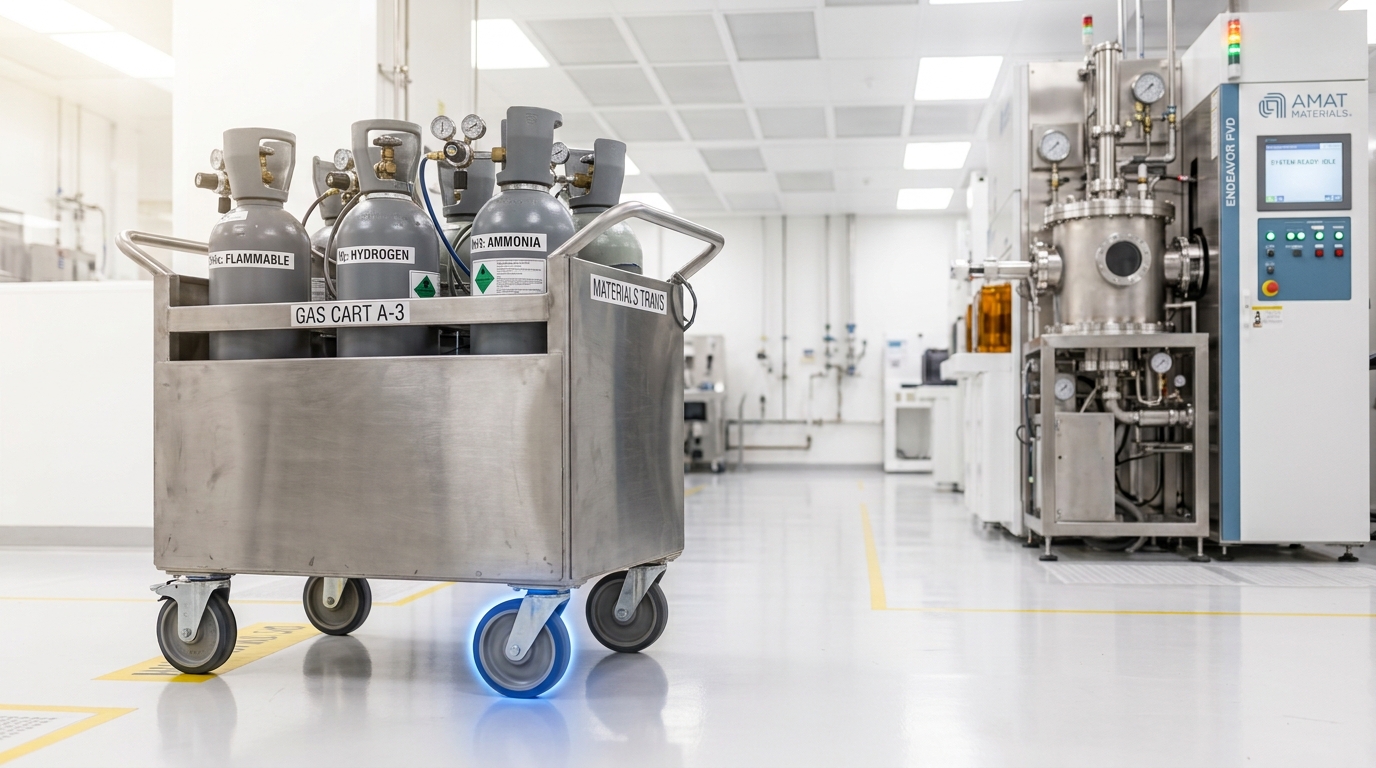
Unlike a chip design decision one company can make unilaterally, adopting a new lithography platform requires an entire fab’s surrounding process ecosystem — resist chemistry, mask technology, metrology tools covered in this cohort’s KLA briefing, and etch processes covered in the Lam Research briefing — to be simultaneously qualified against the new tool’s specific characteristics. That coordination requirement is a large part of why lithography transitions historically take years to reach broad industry adoption even after the core tool itself is technically ready, and it is the more realistic timeline to expect for High-NA EUV’s path from today’s early-adopter milestones to genuinely widespread use across the leading-edge fab landscape this cohort surveys.
The stakes for ASML if the transition slips
A slower-than-expected High-NA rollout would not threaten ASML’s monopoly position — there is still no competing EUV supplier for customers to switch to — but it would delay the specific revenue ramp ASML’s own capital spending and manufacturing capacity have been built around, extending the payback period on one of the most capital-intensive product transitions in the entire semiconductor equipment industry. Readers tracking ASML as a business, not just as a technology story, should watch High-NA-specific revenue disclosures in the company’s own quarterly reporting as the clearest signal of how this transition is actually proceeding.