Four answers to the same shortage
Every engineering group building AI hardware today is solving a version of the same equation: accelerators can do far more arithmetic per second than any practical memory system can feed them, and the gap has been widening for two decades. Gholami and colleagues quantify the trend precisely: peak server hardware FLOPS has scaled at roughly 3.0 times every two years, while DRAM bandwidth managed only 1.6 times and interconnect bandwidth 1.4 times over the same interval [1]. An earlier piece in this series worked through what that gap does inside a single kernel — arithmetic intensity, the roofline, and the reason a fast kernel is fast because of what it never reads. This article asks a narrower and more practical question: given that shortage, what are the actual engineering answers being built at the system level, and what does each one cost?
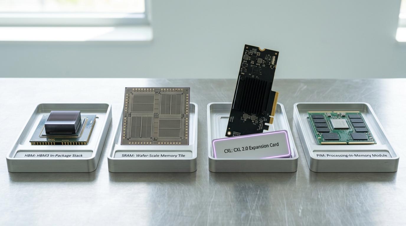
Four answers currently dominate serious engineering conversation. High-bandwidth memory (HBM) stacks DRAM dies in-package next to the compute die and connects them with a very wide, very short bus. Large on-die SRAM architectures — the wafer-scale approach pursued by Cerebras and the dataflow approach pursued by Groq are the clearest public examples — keep the entire working store on the same silicon as the arithmetic units, refusing the trip off-chip altogether. Compute Express Link (CXL) takes the opposite tack: it accepts a longer, slower path in exchange for memory capacity that a single package or socket could never hold, pooled and shared across a fabric. And processing-in-memory (PIM) changes the question rather than the answer, embedding a small amount of compute inside or beside the memory array so that some operations never have to leave it at all.
None of these is a strictly better version of another. Each buys one of capacity, bandwidth, latency, cost or programmability by spending one of the others, and the shortage they are all responding to has not gone away — it has only been distributed across four different trades. What follows works through each trade with the numbers its own advocates and independent measurers have published, and closes on the places where the people who build this hardware for a living still genuinely disagree about which trade is worth making.
The four numbers, and why pins are the hidden constraint
Comparing these approaches usefully requires holding four separate quantities apart, because collapsing them into one “how good is it” score is exactly the mistake that produces indefensible claims. Capacity is how many bytes fit. Bandwidth is how many bytes per second can move once resident. Latency is how long a single access takes before any bytes arrive at all. Programmability is how much of a general-purpose instruction set the store’s neighbourhood actually supports, which determines what fraction of a real workload can benefit from it. Cost sits underneath all four as a fifth constraint deciding how much of any of them a given design can afford.
Bandwidth in particular has a hidden physical driver that explains why these four approaches look so different from one another: pin count. A memory bus’s raw bandwidth is well approximated by
with
Every one of the four approaches below is, underneath its marketing name, a different answer to which side of that equation to spend on. HBM widens
HBM: bandwidth bought by moving the bus in-package
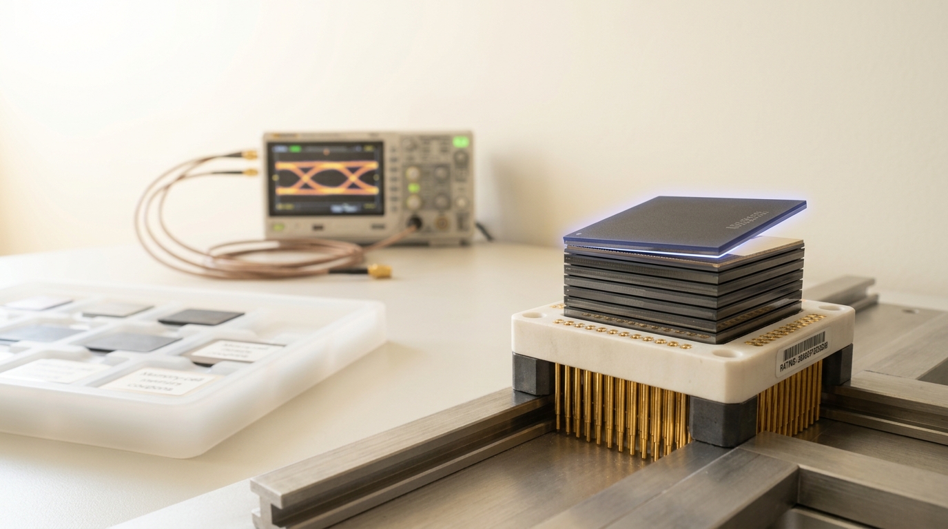
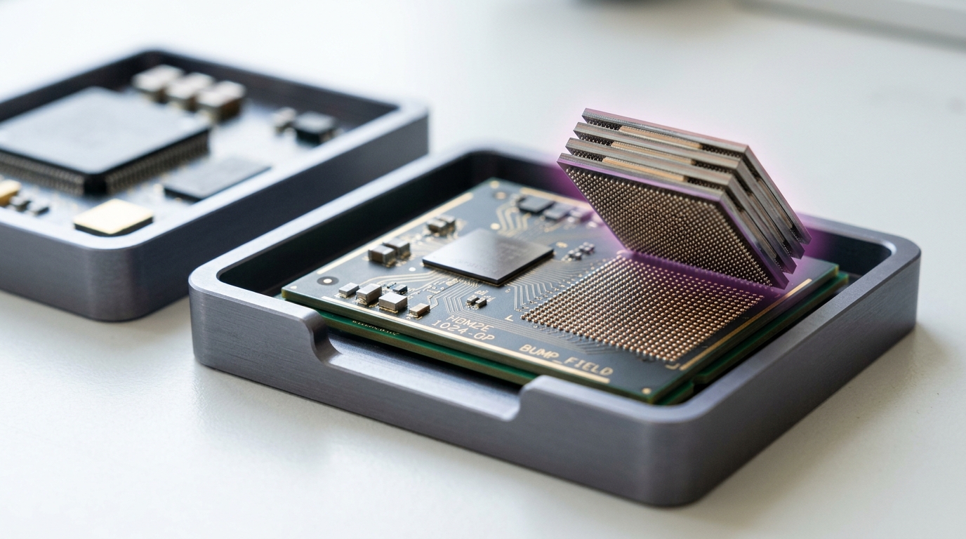
High-bandwidth memory is the industry’s default answer, and it is worth being precise about what JEDEC actually standardised. The HBM3 standard, published as JESD238 in January 2022, specifies a per-pin data rate of up to 6.4 gigabits per second, yielding up to 819 gigabytes per second of bandwidth from a single stack; the standard doubled the number of independent channels to sixteen, with two pseudo-channels each, and supports memory-layer densities from 8 to 32 gigabits, enabling stack capacities up to 64 gigabytes [2]. That is the specification, not a vendor’s marketing claim — JEDEC is the standards body every DRAM and accelerator vendor implements against, and the 819 GB/s figure is a defined maximum for the interface, not a measured result from any particular product.
The mechanism behind that number is the equation above, solved by moving
Large on-die SRAM: bandwidth bought by refusing to leave the die
If HBM widens the bus, the second family of approaches deletes it. Cerebras’s wafer-scale engine keeps the entire compute fabric and its SRAM on a single piece of silicon roughly 46,000 square millimetres in area, with 850,000 cores each holding 48 kilobytes of local SRAM; the company’s own architecture account states each core can sustain two full 64-bit reads and one full 64-bit write per cycle directly from that local memory, and characterises the design as delivering roughly two orders of magnitude more memory bandwidth than a GPU of equivalent silicon area, because the datapath never has to leave the die to find its operands [4]. That is a vendor’s own architectural framing, not an independently measured comparison, and it should be read as such — but the underlying mechanism, zero off-chip hops for the common case, is not in dispute.
Groq’s tensor streaming processor takes a related but distinct route: rather than a single wafer, it distributes 220 mebibytes of SRAM across each chip as logically shared, physically local memory, addressed as a global tensor space and stitched across chips with a deterministic, software-scheduled network rather than a hardware-arbitrated one [5]. The company’s own published system data is unusually candid about where this runs into a wall: a single chip’s global bandwidth to the rest of a scaled system falls from roughly 138 gigabytes per second at very small system sizes, to about 50 GB/s once a system exceeds sixteen chips, to about 14 GB/s once it exceeds 264 chips — the interconnect’s bisection bandwidth is the binding constraint, not the on-die SRAM itself [5]. At full scale, the paper reports a network combining more than 10,440 chips with over two terabytes of aggregate memory reachable in under three microseconds of end-to-end latency [5].
That last pair of numbers is worth sitting with, because it is the honest version of the tradeoff: on-die SRAM buys latency and per-operand bandwidth that HBM cannot match, but a single die’s SRAM capacity is measured in tens of megabytes, so any model that does not fit on one die pays for capacity by adding chips — and the same paper that reports the huge aggregate memory also reports the per-chip bandwidth collapsing by an order of magnitude as chip count grows. The bottleneck HBM was invented to solve does not disappear in an SRAM-centric design; it reappears one level out, at the chip-to-chip interconnect, for any workload too large to fit on a handful of dies.
CXL: capacity bought by leaving the package entirely
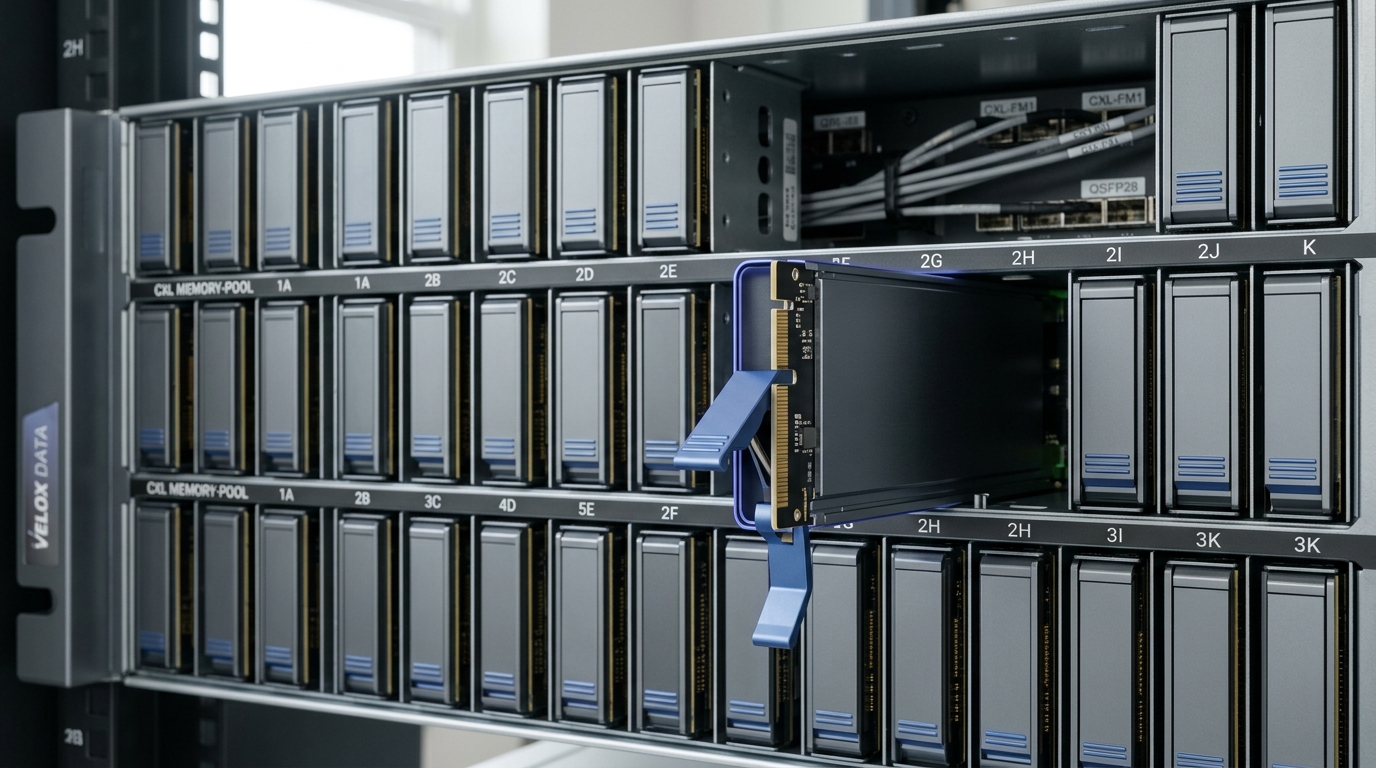
CXL is the approach that stops trying to win the bandwidth fight in the way HBM or on-die SRAM do, and instead spends the equation’s other terms. It is a coherent, load/store-addressable interconnect built on the PCIe physical layer, standardised by the CXL Consortium; the 3.1 specification, released in November 2023, explicitly extends memory sharing and pooling across a fabric “to avoid stranded memory” and to “facilitate memory sharing between accelerators,” while remaining fully backward compatible with CXL 1.0 through 2.0 [3]. The point of the standard is capacity that no single socket or package could hold, pooled and reassigned across machines rather than soldered to one of them.
That capacity is not free. Sun and colleagues built the first comprehensive evaluation of real, shipping CXL memory devices — as opposed to the emulated-via-remote-NUMA-node substitute most earlier research used — across three commercial devices on a current-generation Intel Xeon platform, and their results are a useful correction to intuition built on emulation: true CXL memory can show up to 26 percent lower latency and 3 to 66 percent higher bandwidth efficiency than emulated CXL memory did in prior studies, meaning some of the pessimism in the earlier literature was measuring the wrong thing [6]. Their paper is also explicit about where the physical trade comes from: a CXL memory device connects over PCIe rather than the DDR bus, at roughly three times fewer pins than a DDR5 interface, in exchange for a much longer link latency — on the order of 40 nanoseconds for a PCIe 4.0 hop versus under 1 nanosecond for a native DDR4 link [6]. That is the pin-versus-latency trade the earlier equation predicts: CXL keeps
Whether that trade is worth taking turns out to depend heavily on the workload, and the same paper is blunt about it: naively allocating pages to CXL memory increased tail latency for latency-sensitive, small-object applications such as key-value stores by 10 to 82 percent against keeping everything in local DRAM [6]. Two further systems papers make the same point from the production side. Meta’s Pond, evaluated as a memory-pooling system across its cloud fleet, found that pooling memory across eight to sixteen sockets captured most of the achievable benefit, delivered performance within one to five percent of same-node allocation, and reduced DRAM costs by a reported 7 percent at that scale — a real but modest number, not a transformative one [7]. Meta’s TPP, an OS-level page-placement mechanism built specifically because naive tiering under-performs, reported getting within 1 percent of an all-local-memory baseline and beating the default Linux policy by 18 percent, which is itself evidence that raw hardware capability was not the limiting factor — the placement software was [8]. CXL, in short, buys real capacity, but only after software does real work to decide what belongs on the far side of the fabric.
Processing-in-memory: bought by moving the compute instead of the data
The fourth approach does not try to widen
Samsung’s HBM-PIM, demonstrated commercially as Aquabolt-XL, integrates a programmable compute unit into each memory bank of an otherwise standard HBM2 device, described by the company as requiring no change to the host memory controller — an HBM-PIM stack is a drop-in replacement for a conventional HBM2 stack from the processor’s point of view [9]. The mechanism is straightforward: by performing simple arithmetic where the data already sits, in parallel across many banks at once, the design can exploit up to four times higher in-DRAM bandwidth through multi-bank parallelism than routing every value out to the host processor first [9]. Samsung’s own reported system-level results are specific about where this helps and where it does not: for memory-bandwidth-bound workloads — the company names speech recognition, natural-language translation and recommendation — the system delivered over twice the performance while cutting energy consumption by more than 70 percent; the same materials are explicit that compute-bound workloads such as computer vision see little of that benefit, because those workloads were never waiting on the memory bus in the first place [9]. That asymmetry is the whole story of PIM in one sentence: it is a targeted fix for a specific bottleneck, not a general accelerator.
UPMEM’s approach generalises the idea to standard, general-purpose DRAM rather than HBM specifically, integrating simple in-order cores — DRAM Processing Units — directly into commodity DRAM technology, and Gómez-Luna and colleagues built the first comprehensive independent benchmark suite against real UPMEM hardware, evaluated on two actual deployed systems of 640 and 2,556 DPUs [10]. Their motivation cites the scale of the problem PIM is aimed at: prior studies of data-centric and consumer workloads found data movement between memory and processor cores accounting for as much as 62 percent of total system energy in some reported measurements [10]. The paper’s methodological framing is as telling as its results: it exists specifically to characterise architectural limits and produce programming recommendations and “suggestions and hints for hardware and architecture designers of future PIM systems” [10] — language that only makes sense if success on real DPU hardware is workload-dependent rather than automatic, which is exactly what an independent benchmark of a genuinely new class of hardware should be expected to find.
What both PIM efforts share is a programmability ceiling. The compute embedded in or beside a DRAM bank is necessarily simple — narrow SIMD lanes or small in-order cores, no coherent cache, limited addressing — because DRAM process technology and the area and power budget inside a memory die cannot support a full out-of-order core. PIM therefore buys bandwidth and energy efficiency for the narrow slice of a workload that is simple, data-parallel and genuinely memory-bound, and buys little for everything else, once data has to be reshaped to fit the DPU’s programming model.
What a real accelerator actually assembles
None of the four sections above describes a system anyone ships in isolation. A contemporary AI accelerator composes several of these answers on top of each other, for a reason the earlier article in this series already established: capacity and bandwidth are separate constraints with separate symptoms, and a real workload — serving a large language model’s key-value cache is the canonical case — hits both at once. The KV cache for a single sequence grows as
with
This is why the four approaches in this article are best read as a shared vocabulary rather than a shortlist to choose one from. A serving accelerator typically holds weights and the resident portion of the KV cache in HBM for bandwidth, may spill a colder or overflow portion of that cache to CXL-pooled memory for capacity once local HBM is exhausted, and — where the workload has enough of a genuinely memory-bound, data-parallel component — may lean on a PIM-equipped memory tier for that specific slice of the work. Wafer-scale and dataflow SRAM-centric designs make a more concentrated bet: they minimise capacity requirements per chip deliberately, accepting that a large model must be partitioned across more chips than an HBM-based design would need, in exchange for latency and bandwidth per operand that neither HBM nor CXL can approach. All four answers are visible, simultaneously, inside a single modern serving fleet; none of them replaces the others.
Where the disagreement actually lies
Three disagreements are real, current and not resolved by the numbers above, and it is worth stating each one as a disagreement rather than pretending the evidence already settles it.
First, whether CXL memory pooling matters for AI workloads specifically, or mainly for general cloud memory economics. Pond’s production evaluation is a cloud-fleet memory-consolidation result, not an AI-training or AI-serving result, and its own authors report a real but modest 7 percent DRAM cost saving [7]. Sun and colleagues’ finding that naive CXL allocation actively hurts latency-sensitive workloads by double-digit percentages cuts against treating CXL as a drop-in bandwidth or capacity expander for AI serving without new software [6]. Some architects read this as CXL’s natural home being cold KV-cache and model-weight overflow tiers, where latency tolerance is high; others read the same evidence as showing CXL has not yet demonstrated a compelling AI-specific win at all, only a general-purpose memory-economics one. Both readings are consistent with the published numbers; the disagreement is about which future workload mix CXL will actually be tuned for, which is not yet observable.
Second, whether large on-die SRAM architectures are a broadly competitive path or a narrow one. Groq’s own published data shows per-chip global bandwidth falling by roughly an order of magnitude as system scale grows past a few hundred chips [5], and Cerebras’s bandwidth advantage is stated by the vendor itself as a comparison normalised to equivalent silicon area against a GPU, not a comparison at matched cost, power or programmability [4]. One view in the field treats this as a genuine ceiling that confines SRAM-centric designs to models and batch sizes that fit within a bounded chip count. The opposing view treats the same evidence as irrelevant to the workloads these architectures actually target — low-batch, latency-critical inference on models chosen to fit the SRAM budget — where the comparison to a capacity-unconstrained accelerator was never the right comparison to begin with. Neither camp disputes the numbers; they disagree about which workload class is the fair test, which is exactly why this article does not attempt to rank Cerebras, Groq, HBM-based accelerators and CXL-expanded systems against one another on a single benchmark: the benchmarks that would settle it are not run on comparable terms.
Third, whether PIM is a durable architectural category or a narrow accelerator for a shrinking set of kernels. Samsung’s own chart draws the line explicitly — large wins on memory-bound workloads, little or none on compute-bound ones [9] — and UPMEM’s independent benchmark suite exists precisely because that line is not obvious in advance for a given workload [10]. One position holds that as arithmetic-intensity requirements keep falling for a growing share of inference workloads — long-context attention, sparse retrieval, embedding lookups — the addressable slice for PIM grows and the technology moves from niche to default. The opposing position notes that every commercially available PIM product to date has shipped as a specialised part attached to a specific workload rather than a general-purpose memory replacement, and that the programmability constraints inherent to embedding compute inside a DRAM process are not obviously solvable by better software alone. This article takes no side; both positions cite the same primary sources.
Predictions, with the observations that would falsify them
These are forecasts, separated from the sourced comparison above. Horizon: 15 August 2029. The assumptions are that the FLOPS-versus-bandwidth divergence documented by Gholami and colleagues continues, and that no single memory technology closes the gap by an order of magnitude in that window.
One. No single one of these four approaches will displace the other three; production accelerators in 2029 will still combine at least two of HBM, CXL and on-die SRAM in the same system. Disconfirmed if a mainstream accelerator generation ships with only one memory technology and no tiering at all.
Two. CXL deployment for AI-specific workloads will remain concentrated in capacity-tolerant, latency-tolerant roles — cold KV cache, weight overflow, batch offline inference — rather than the hot path of interactive serving. Disconfirmed if a major inference provider publishes production evidence of CXL-pooled memory on the latency-critical hot path of interactive serving at parity with local HBM.
Three. At least one further commercial PIM product will ship attached to a narrow, named workload class rather than as a general-purpose memory replacement, continuing the pattern set by Aquabolt-XL and UPMEM. Disconfirmed if a PIM product ships and is marketed as a general-purpose memory replacement with no named target workload.
Four. Published comparisons between SRAM-centric and HBM-centric accelerators will increasingly report matched-cost or matched-power figures rather than raw per-chip or per-area bandwidth, because the unmatched comparisons in this article’s own sources will have become recognised as insufficient on their own. Disconfirmed if leading vendor and academic comparisons in 2029 still report normalised-bandwidth figures without any matched cost or power basis.
What to take away
Four different engineering communities looked at the same widening gap between arithmetic and memory bandwidth and made four different, defensible bets. HBM widened the bus by moving it into the package. Large on-die SRAM deleted the bus for a bounded amount of data, and paid for it in per-chip capacity. CXL kept the bus narrow and accepted latency in exchange for pooled capacity no package could hold alone. Processing-in-memory stopped trying to move bytes faster and moved a sliver of compute to meet them instead.
None of the sources cited above supports ranking these four against each other on a single number, and several of them explicitly warn against exactly that: Samsung’s own PIM data draws a line between workloads it helps and workloads it does not; Sun and colleagues’ CXL measurements show naive use actively hurting the workloads it was supposed to help; Groq’s own bandwidth profile shows the constraint it solved on-die reappearing off-chip at scale. The honest comparison is not which approach wins, but which term of the same underlying trade — capacity, bandwidth, latency, cost, programmability — a given workload is actually short of, and which of the four answers was built to spend on exactly that term.