An accelerator running a large language model spends most of a decoding step doing almost nothing arithmetically interesting. Its floating-point units, capable of hundreds of trillions of operations per second, sit substantially idle while the chip waits for its memory system to deliver the next set of weights and cached state. This is not an implementation bug. It is the predictable consequence of a ratio — how many arithmetic operations a workload performs per byte moved from memory — set against a second ratio that describes what the hardware can actually supply. Getting that mechanism right, rather than reaching for “AI needs more memory” as an unexamined slogan, requires walking through four things in order: how a memory stack physically delivers its bandwidth, what the ratio that governs efficiency actually measures, how a growing cache of intermediate state consumes the same budget the weights need, and what pooling memory across a fabric changes and does not change.
How an HBM stack delivers bandwidth in the first place
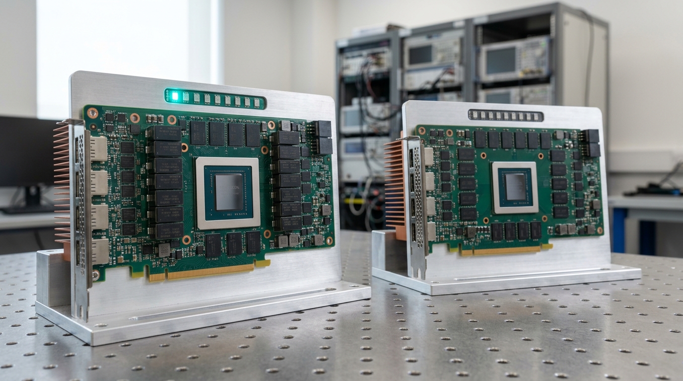
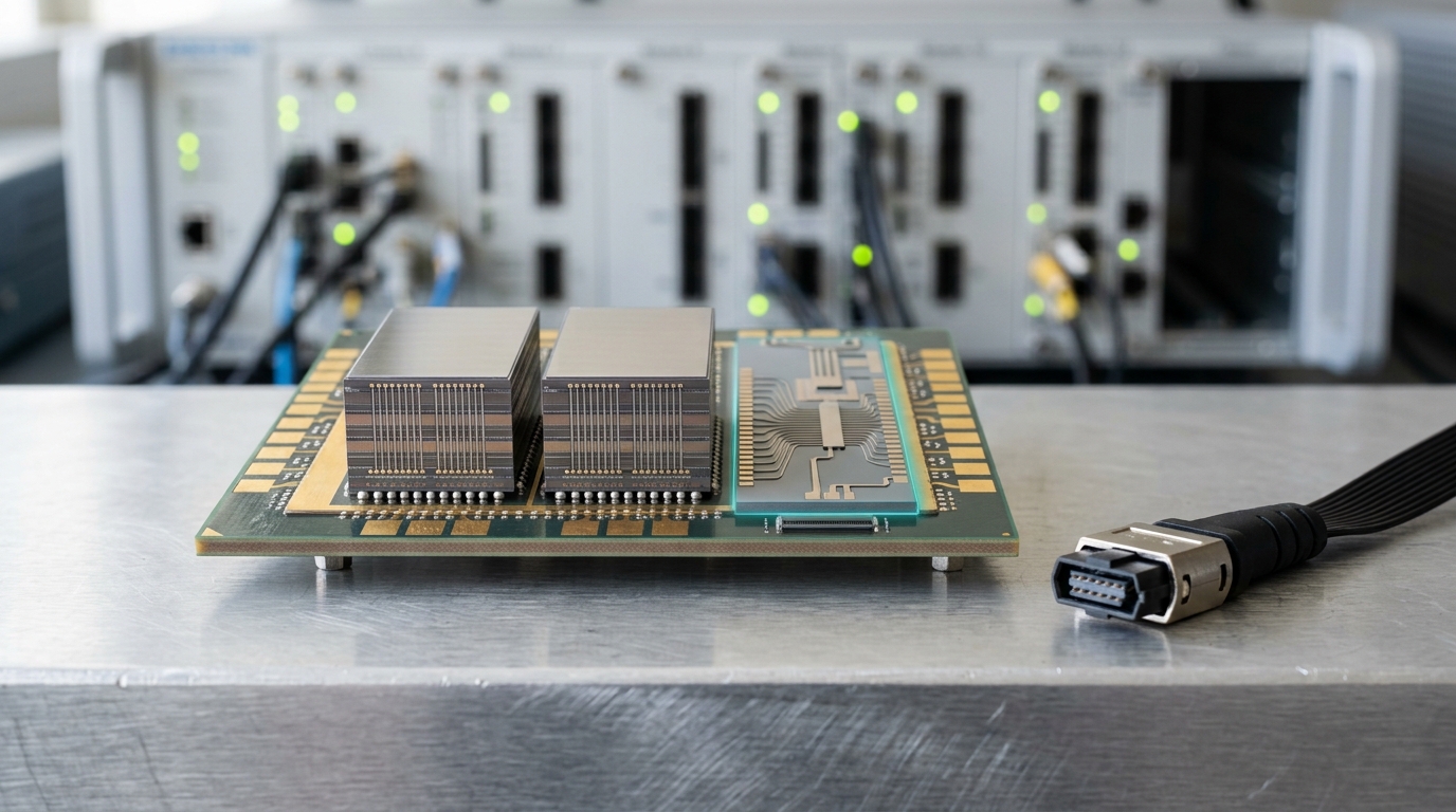
High Bandwidth Memory reaches its throughput by trading distance and pin count against depth. A conventional DRAM module talks to its host over a modest number of high-speed serial-like pins running at very high per-pin data rates across centimetres of PCB trace. HBM inverts that trade: it uses a very wide, comparatively slow-per-pin interface — thousands of parallel signal paths — running only millimetres, because the DRAM dies are stacked directly on top of one another and connected vertically by through-silicon vias, then mounted next to the compute die on a shared silicon interposer [1]. The JEDEC HBM4 standard, published as JESD270-4 in April 2025, specifies a 2,048-bit-wide interface per stack running at up to 8 gigabits per second per pin, doubling the interface width’s effective channel count to 32 independent channels (each split into two pseudo-channels) versus HBM3’s 16, for a stated total of up to 2 terabytes per second per stack [1]. That figure is a JEDEC specification ceiling, not a shipped-part measurement; actual delivered bandwidth on a given accelerator depends on how many stacks are attached and how the memory controller schedules across them.
The stacking itself is the other half of the mechanism. SK hynix’s 12-layer HBM3E, which entered volume production in 2024, reaches 36 gigabytes of capacity per stack by bonding twelve separately thinned DRAM dies to the same overall stack height as the previous eight-layer generation, achieved by thinning each die roughly 40 percent and connecting the stack through-silicon vias vertically rather than adding thickness [8]. This is a vendor-reported manufacturing achievement, not an independent measurement, but it illustrates the physical lever precisely: bandwidth per stack scales with how many parallel channels and how much per-pin speed JEDEC’s electrical specification allows, while capacity per stack scales with how many dies can be thinned and stacked without exceeding the same footprint.

A production accelerator such as NVIDIA’s H100 attaches several such stacks around the compute die; NVIDIA’s own published specification for the SXM configuration lists 80 gigabytes of HBM3 capacity delivering 3.35 terabytes per second of aggregate memory bandwidth to that single package [7]. That number is the sum across all attached stacks and the realized figure NVIDIA states for the finished product, distinct from the JEDEC per-stack ceiling above — a useful reminder that a chip’s advertised bandwidth is a system-level integration result, not a direct readout of the memory standard alone.
None of this bandwidth is free of a physical cost. Every via, every micro-bump, every layer of the interposer is a place a stack can fail to bond, and the entire assembly sits directly on the reticle-limited compute die’s thermal budget, since the DRAM stacks and the logic die share a package and a cooling solution. That constraint is a separate discussion from this article’s focus — it belongs to the packaging and yield side of the story — but it is worth naming here because it explains why HBM capacity and bandwidth have grown by re-engineering the stack (thinner dies, more layers, wider per-stack interfaces) rather than simply adding more, larger, independent memory chips around the die the way a conventional server motherboard adds DIMM slots.
What “arithmetic intensity” actually measures, and why decoding sits on the wrong side of it
The roofline model, introduced by Williams, Waterman, and Patterson in 2009, gives the concept its formal shape. It plots two independent ceilings on the same chart: the chip’s peak arithmetic throughput (operations per second) on one axis, and its peak memory bandwidth (bytes per second) combined with a workload-specific ratio on the other. That ratio — arithmetic intensity — is defined as the number of floating-point operations performed per byte of data moved between memory and the arithmetic units [4]. A workload’s achievable throughput is bounded by whichever ceiling it hits first:
When a workload’s intensity
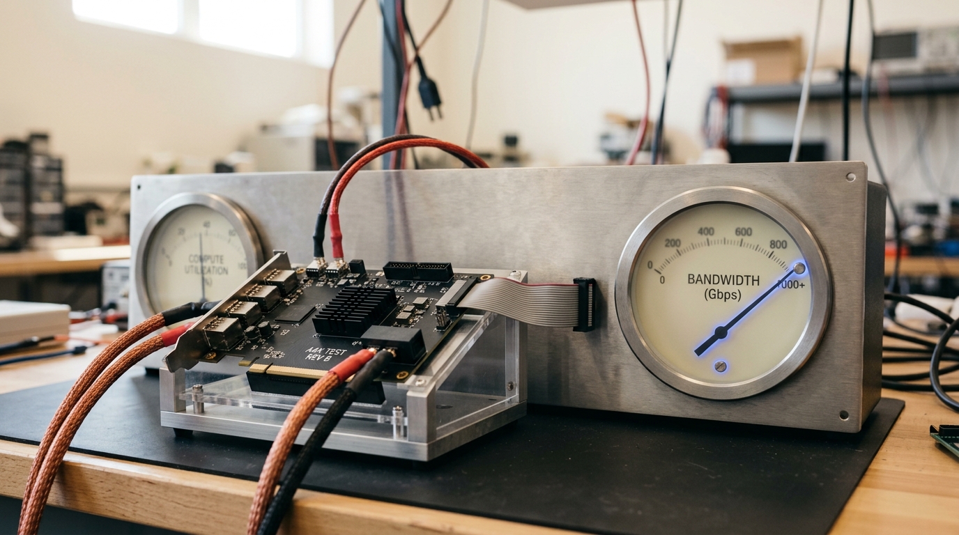
Autoregressive decoding — generating one token, appending it to the sequence, and generating the next — sits firmly on the memory-bound side of that line. During a single decode step, an accelerator must read essentially the entire set of model weights (and the accumulated key-value cache, discussed below) from memory to produce one new token per sequence in the batch, performing comparatively few arithmetic operations per byte read because the batch of “useful work” per weight read is thin unless many sequences are batched together. Training, or a large batched prefill pass over a long prompt, looks different: the same weights are reused across many tokens and many sequences in one pass, so the arithmetic-operations-per-byte-moved ratio rises and the workload can approach the compute-bound regime. This is why the same accelerator can be compute-bound during training and memory-bound during single-user, low-batch inference — the hardware has not changed, but the ratio the workload presents to it has. It is also why serving providers batch many concurrent requests together at the same decode step: batching raises the amount of arithmetic performed per byte of weight read, pushing the effective intensity of the aggregate workload up toward the compute-bound side, at the cost of added latency for any one request in the batch. This is an architectural trade-off with a documented mechanism, not a vendor claim; it follows directly from the roofline relationship above.
How a growing key-value cache consumes the same bandwidth budget
Transformer-based generation keeps a running cache of the key and value vectors computed for every token already in the sequence, so each new token’s attention computation can look back over everything before it without recomputing those vectors from scratch. This key-value (KV) cache grows linearly with sequence length and linearly with the number of concurrent sequences being served, and — critically for the bandwidth-wall argument — it must be read from memory at every decoding step for every active sequence, alongside the model weights [5]. The 2023 PagedAttention paper by Kwon et al. reports that for a single LLaMA-13B sequence, the KV cache can require up to 1.7 gigabytes of storage, and that naive serving systems, which reserve a cache slot sized for a sequence’s maximum possible length up front, waste an estimated 60 to 80 percent of allocated KV-cache memory to fragmentation and over-reservation, since actual sequence lengths vary unpredictably and most of the reserved space goes unused [5].
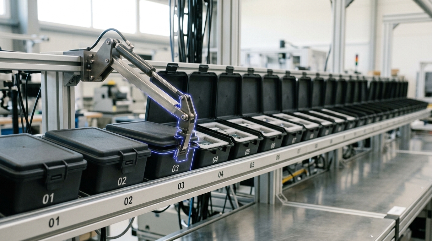
PagedAttention’s fix borrows directly from operating-system virtual memory: instead of reserving one large contiguous block per sequence, it manages the cache in small fixed-size blocks that can be allocated non-contiguously and mapped on demand, the same way a paging system maps virtual pages to physical frames [5]. The vLLM serving engine built around this technique reports, in its own project announcement, up to 24 times higher throughput than the Hugging Face Transformers baseline and up to 3.5 times higher throughput than Hugging Face’s Text Generation Inference, with reported memory waste in the cache reduced to under 4 percent — figures that are the vLLM project’s own reported benchmarks rather than an independent third-party measurement, and specific to the baselines and models tested [6]. The mechanism, independent of whose benchmark is used to size it, is the important part for this article: every block of cached key-value state occupies memory bandwidth on every subsequent step for as long as its sequence is active, competing directly with the weight reads described above. A long-context request does not just cost more memory capacity — it costs more of the same bandwidth budget that arithmetic intensity showed is already the binding constraint on decoding.
This is also why techniques that reduce the number of key-value heads a model computes (grouped-query attention and its relatives) or that compress cached vectors are, mechanically, bandwidth-reduction techniques before they are anything else: shrinking the cache shrinks the number of bytes that must be read per decoding step, which directly raises the workload’s effective arithmetic intensity for a fixed weight-read cost. That is an architectural choice made at model-design time, separate from the serving-system engineering PagedAttention addresses, but the two attack the same bottleneck from different ends.
It is worth being precise about what block-based cache management does and does not fix, because the two are easy to conflate. PagedAttention and its block-allocation approach address a bookkeeping inefficiency: memory reserved for a sequence but never actually used because the sequence turned out shorter than its worst-case allocation, or memory that could be shared between sequences (for instance, several parallel samples generated from the same prompt sharing an identical prefix) but was duplicated instead because the allocator had no mechanism for reference-counted sharing [5]. That is a real and measurable waste, and eliminating it recovers usable capacity and, indirectly, some bandwidth, since blocks that are never allocated are never subsequently read. But it does not change the fact that every block that is legitimately in use — a real token’s real key and value vectors, actually needed for a real future attention computation — must still be read from memory on every step for as long as that sequence stays active. A perfectly bookkept cache for a ten-thousand-token conversation still reads ten thousand tokens’ worth of key-value state per decoding step; better allocation removes the waste around that number, it does not remove the number itself. Distinguishing “wasted allocation” from “necessary but expensive” is the difference between a serving-engineering fix and an architectural one, and conflating them is a common source of overclaiming about how much a paging scheme alone can do about the underlying bandwidth wall.
What CXL memory pooling actually changes
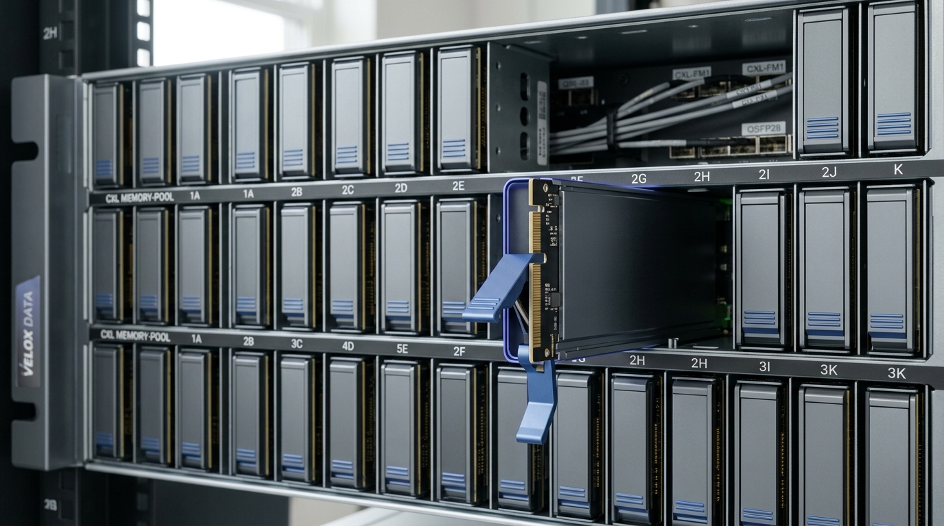
Compute Express Link is a cache-coherent interconnect standard that runs over the same physical layer as PCIe and defines three protocols: CXL.io for conventional I/O, CXL.cache for coherent caching by an attached device, and CXL.mem, which lets a host access memory that physically lives on a separate device as if it were local, coherent memory [2]. The CXL Consortium’s own explanation of pooling describes a dedicated fabric manager that dynamically allocates capacity from a shared pool of memory devices among multiple attached hosts, providing each host a guaranteed slice, memory isolation between hosts, and the ability to expand or shrink a host’s addressable capacity to match its current workload rather than a capacity fixed at the server’s build time [3]. The CXL 3.1 specification, released in November 2023, extended this further by adding peer-to-peer direct memory access between devices and enhancements that let multiple hosts coherently share a single memory space on a CXL 3.1 device, while remaining backward compatible with CXL 2.0, 1.1, and 1.0 [2].
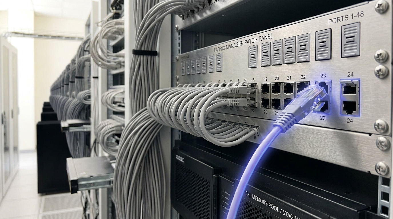
The concrete problem pooling solves is stranded capacity: in a fleet of servers each built with a fixed amount of local DRAM, some machines run out of memory while others sit with capacity idle, because workload demand does not match the static allocation any single server was provisioned with. A shared, fabric-attached pool lets a fabric manager hand out more capacity to whichever host needs it at that moment and reclaim it when the workload’s demand drops, improving fleet-wide utilization without over-provisioning every individual server [3]. That is a real, mechanism-level benefit, and it is distinct from — and should not be confused with — a bandwidth benefit. CXL.mem traffic travels over the CXL fabric link rather than the short, wide, on-package path an HBM stack uses; a fabric-attached memory pool sits at a materially higher latency and, for equivalent link width, typically a lower achievable bandwidth than a directly attached DRAM channel, let alone an HBM stack a few millimetres from the compute die. Pooling is a capacity-and-utilization mechanism, not a bandwidth-wall mechanism: it changes how much memory a workload can address and how efficiently that capacity is shared across a fleet, but it does not change the per-byte cost of the memory-bound decoding step described above, and in practice it adds a slower tier below HBM and local DRAM rather than replacing the need for either.
This is the honest place to separate vendor framing from mechanism. CXL Consortium materials describe pooling and sharing as improving “efficient memory allocation” and reducing total cost of ownership by cutting stranded capacity [3] — a claim about fleet-level utilization economics, made by the standards body promoting the technology, and worth attributing as such rather than treating as an independent efficiency measurement. Separately, near-memory computing — placing a small amount of fixed-function or programmable logic on a buffer chip physically adjacent to a DRAM stack, so that simple operations (accumulation, reduction, some sparse-gather patterns) can be performed without moving every byte all the way to the main compute die — is a complementary, still largely research- and early-product-stage approach to the same underlying problem: it does not increase the bandwidth of the link to the main die, it reduces how many bytes need to cross that link at all by doing a small amount of arithmetic locally first. It is a narrower, more specialized technique than either HBM’s wide stacking or CXL’s pooling, applicable to a limited set of operations that can be pushed down to simple logic, and it should not be conflated with either of the other two mechanisms.
Putting the four mechanisms together
None of these four mechanisms compete with each other; they sit at different points in the same system. HBM stacking is what makes a large bandwidth number physically deliverable to one compute die in the first place, by shortening the electrical path and widening the bus rather than by any exotic new physics. Arithmetic intensity is the ratio that determines, for a given workload, whether that delivered bandwidth or the chip’s arithmetic throughput is the binding constraint — and autoregressive decoding, structurally, tends to sit on the bandwidth-bound side of that line unless batching raises its effective intensity. The KV cache is a second, growing consumer of that same bandwidth budget, one whose size is a direct function of sequence length and concurrency rather than of model size alone, and whose bookkeeping (paged, block-based allocation rather than static reservation) has an independently documented effect on how much of the available cache capacity is actually wasted. And CXL pooling addresses a fourth, largely separate problem — stranded capacity across a fleet — by trading a longer, fabric-attached path for flexible, shared addressability, which is valuable for utilization and total cost of ownership but does not relax the bandwidth ceiling that governs any individual decoding step.
Reading vendor announcements about any one of these four mechanisms in isolation risks conflating them: a JEDEC bandwidth ceiling is not a shipped product’s measured bandwidth; a serving framework’s own reported throughput multiplier is not an intensity measurement; and a standards consortium’s utilization pitch for pooling is not a bandwidth claim. Keeping the four mechanisms and the three kinds of claim — specification, vendor-reported measurement, and architectural analysis — separate is what makes it possible to say something concrete about why an accelerator’s arithmetic units spend a decoding step waiting, rather than reaching for “memory bandwidth is the new bottleneck” as an assertion that explains nothing about its own mechanism.
A brief note on what would change this picture, stated as a scenario rather than a prediction. If a near-memory or in-memory compute approach matured to the point of handling a meaningful share of attention’s memory-bound operations directly on a buffer chip beside the DRAM — not merely simple accumulation, but a usable fraction of the key-value read-and-score step itself — the effective arithmetic intensity of decoding as seen by the main compute die would rise, because fewer of the bytes behind that computation would need to cross the package boundary at all. The observable indicator would be a production accelerator whose datasheet reports a near-memory compute throughput figure alongside its HBM bandwidth figure, the way GPUs today report both tensor and memory bandwidth numbers; the disconfirming observation would be continued generations of accelerators where every additional bandwidth increment comes solely from wider or faster HBM interfaces, with near-memory logic remaining confined to research prototypes and narrow fixed-function offload rather than general serving workloads. As of this writing, published accelerator roadmaps and datasheets fall entirely in the second camp: HBM4’s JEDEC-specified doubling of channel count is a wider-and-faster-interface improvement, not a near-memory-compute one [1], and no production LLM-serving deployment described in the sources used here reports offloading a meaningful share of attention computation to logic co-packaged with the DRAM itself.