Four bets about where control lives
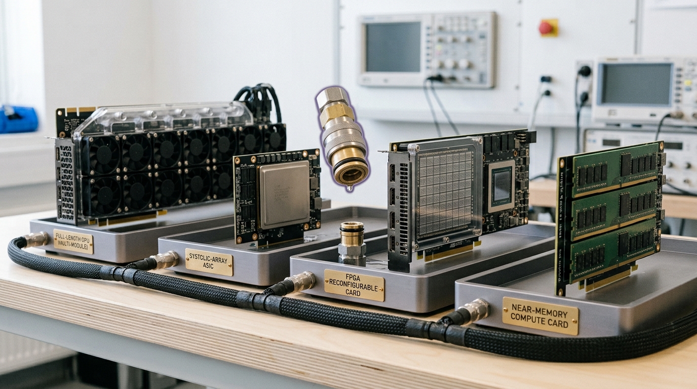
Every AI accelerator design starts from the same constraint and answers it differently. Dense linear algebra is cheap to compute and expensive to feed, so the interesting decision is rarely how much arithmetic to build — it is where the control over that arithmetic’s schedule is allowed to live. A general-purpose GPU keeps control mostly in a hardware scheduler that decides at runtime, thread by thread, so it can be reprogrammed for almost any workload without a new chip. A systolic-array ASIC moves that control into the physical regularity of the array itself, fixing the schedule so completely that data simply propagates through a grid on a clock edge. A dataflow or reconfigurable architecture puts control in the compiler: the mapping from computation graph to physical unit is worked out once, ahead of time, and the silicon executes that plan with as little runtime decision-making as it can get away with. Near- and in-memory compute goes further still and asks whether arithmetic can be pushed into the memory array itself, so that scheduling data movement to a separate compute unit stops being a meaningful question for a slice of the workload.
This article works through those four families in turn, then asks what a reader should do with the comparison. Two ground rules apply throughout, and this is exactly the article where they are easiest to break. First, a vendor’s own generational comparison — this chip against the same company’s previous chip — is evidence about that company’s roadmap and does not compose across vendors. Second, where the people who build these things genuinely disagree about which approach wins for a given workload, the honest move is to describe the disagreement rather than adjudicate it from outside. A reader who wants a single ranking of GPU versus ASIC versus reconfigurable fabric versus processing-in-memory should distrust anyone, including this article, who offers one without immediately qualifying it by workload, precision, batch size and measurement date.
The general-purpose answer: SIMT and the GPU
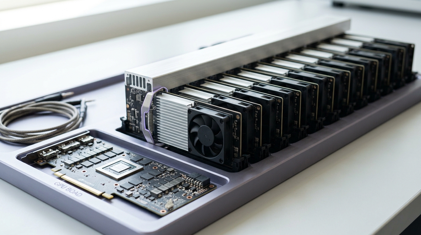
The GPU’s architectural bet is that flexibility is worth paying for in silicon, because the workload mix a buyer will actually run is not known at tape-out time. Its execution model — single-instruction-multiple-thread, SIMT — organises many lightweight threads into warps that execute the same instruction in lockstep while a hardware scheduler decides, cycle by cycle, which warp runs next and how to hide the latency of one warp’s memory stall behind another warp’s arithmetic. Nothing about that scheduling decision is fixed at design time; it happens fresh, for every kernel, on every run.
That flexibility costs silicon area and design complexity spent on things a fixed array does not need — instruction issue, occupancy management, warp schedulers, register-file banking — and the industry’s response has been to keep the general core but attach an increasingly large, increasingly systolic-like matrix unit beside it. NVIDIA’s own account of its Hopper architecture describes fourth-generation Tensor Cores delivering, in the company’s words, “2x the MMA (Matrix Multiply-Accumulate) computational rates of the A100 SM on equivalent data types, and 4x the rate of A100 using the new FP8 data type,” alongside additions whose entire purpose is feeding those units faster — an asynchronous Tensor Memory Accelerator, thread block clusters that let one streaming multiprocessor read another’s shared memory directly, and a jump in combined shared memory and L1 capacity to 256 KB per SM [11]. Those are the vendor’s own disclosures about its own part, and they describe a design converging, generation over generation, toward the systolic family’s proportions without abandoning the general-purpose core that makes the chip programmable for everything else a datacenter needs a GPU for. That dual identity — general-purpose core plus increasingly specialised matrix engine — is a large part of why the GPU still occupies the centre of the market despite ASICs built purely for matrix multiplication existing since at least 2015.
The regular-grid answer: the systolic array
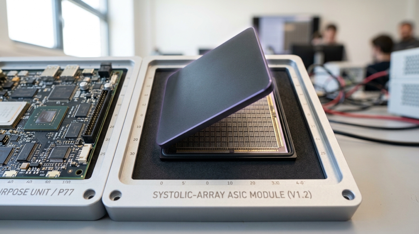
A systolic array answers the same question by refusing to keep a scheduler around at all. The idea is four decades old: H. T. Kung’s 1982 paper describes a system in which “data flows from the computer memory in a rhythmic fashion, passing through many processing elements before it returns to memory, much as blood circulates to and from the heart,” and argues that this rhythmic, multiply-reused data movement is what lets a special-purpose array beat a general-purpose computer on I/O-bound problems without needing faster memory, because each datum, once fetched, is used by many processing elements before it is retired [2]. Kung is explicit that the appeal is economic as much as architectural: a design built from a few simple, regular, repeated cell types is cheap to verify and lay out, and its regularity is what makes it “easy to reconfigure to meet various outside constraints” at the design stage, even though the resulting chip has no runtime reconfigurability at all [2].
Google’s Tensor Processing Unit is the clearest production instance of the idea applied to neural networks. The 2017 paper describing the first-generation TPU documents a 65,536-element 8-bit multiply-accumulate matrix unit fed by a 28 MiB software-managed on-chip memory, reaching a peak of 92 TeraOps per second, and its authors report that on their production inference workloads the chip achieved 15 to 30 times the throughput and 30 to 80 times the performance-per-watt of a contemporary Intel Haswell CPU and NVIDIA K80 GPU [1]. That comparison is worth reading as Google’s own measurement, made in 2017 against parts already a generation or more behind at the time — it says a great deal about what a systolic array bought against 2015-era general-purpose silicon on that specific workload set, and nothing directly about how a current-generation systolic ASIC compares with a current-generation GPU, since the comparison was never repeated on matched contemporary hardware by an independent party, and vendor generational claims of this kind do not transfer across companies or years.
What does transfer is the structural argument. Because the TPU’s array has no instruction fetch, no branch prediction and no per-operation scheduling decision inside the grid, essentially all of its area and power budget goes to arithmetic and the on-chip memory that feeds it, rather than to control logic a general-purpose core carries every cycle whether or not that cycle does useful work. The array pays for that efficiency with rigidity: very good at the one operation it was built for, dense matrix multiplication at the precision it supports, and comparatively poor at anything shaped differently — irregular sparsity, ragged matrix dimensions, control-heavy code — because there is no scheduler available to route around the mismatch.
The compiler-scheduled answer: dataflow and reconfigurable fabric
A third family tries to keep the systolic array’s efficiency argument — no runtime scheduling logic burning power every cycle — while keeping more of the GPU’s ability to run more than one kind of computation. The bet is that if a compiler can work out a complete, static execution plan ahead of time, the hardware does not need the reactive machinery — caches, branch predictors, out-of-order issue, arbiters — that a general-purpose core carries to cover for not knowing what comes next.
Groq’s Tensor Streaming Processor is the most explicit statement of that bet. Its architects describe a “functionally-sliced microarchitecture with memory units interleaved with vector and matrix deep learning functional units in order to take advantage of dataflow locality,” built on a “simple and deterministic processor with producer-consumer stream programming model,” and state plainly that the design achieves its predictability “by eliminating all reactive elements in the hardware (e.g. arbiters, and caches)” [3]. Every scheduling decision a GPU’s hardware would make at runtime is instead made once by Groq’s compiler and baked into the instruction stream; the chip’s job is only to execute that stream in lockstep. The paper’s authors report an early ResNet-50 result of 20,400 images per second at a batch size of one on their first silicon implementation, a four-times improvement over the GPUs and accelerators they compared against at the time — again a vendor’s own dated comparison, but a real demonstration that eliminating scheduling overhead matters most at batch size one, exactly the regime where a scheduler has the least work to overlap [3].
A closely related academic line pushes the same static-plus-dynamic split into genuinely reconfigurable hardware rather than a fixed streaming array. Plasticine, a coarse-grained reconfigurable architecture built from repeated Pattern Compute Units and Pattern Memory Units, executes in two phases: “a static configuration phase establishes the datapath and control structures before execution begins, while a dynamic dataflow phase allows data to move through the preconfigured hardware at runtime,” according to its authors, who designed it so one chip could be reconfigured into different spatial layouts for different parallel patterns rather than fixing one layout permanently in the die [4]. That reconfigurability is what a systolic ASIC cannot offer: the same silicon can, in principle, be redrawn into a different circuit for a workload whose shape was not known at tape-out.
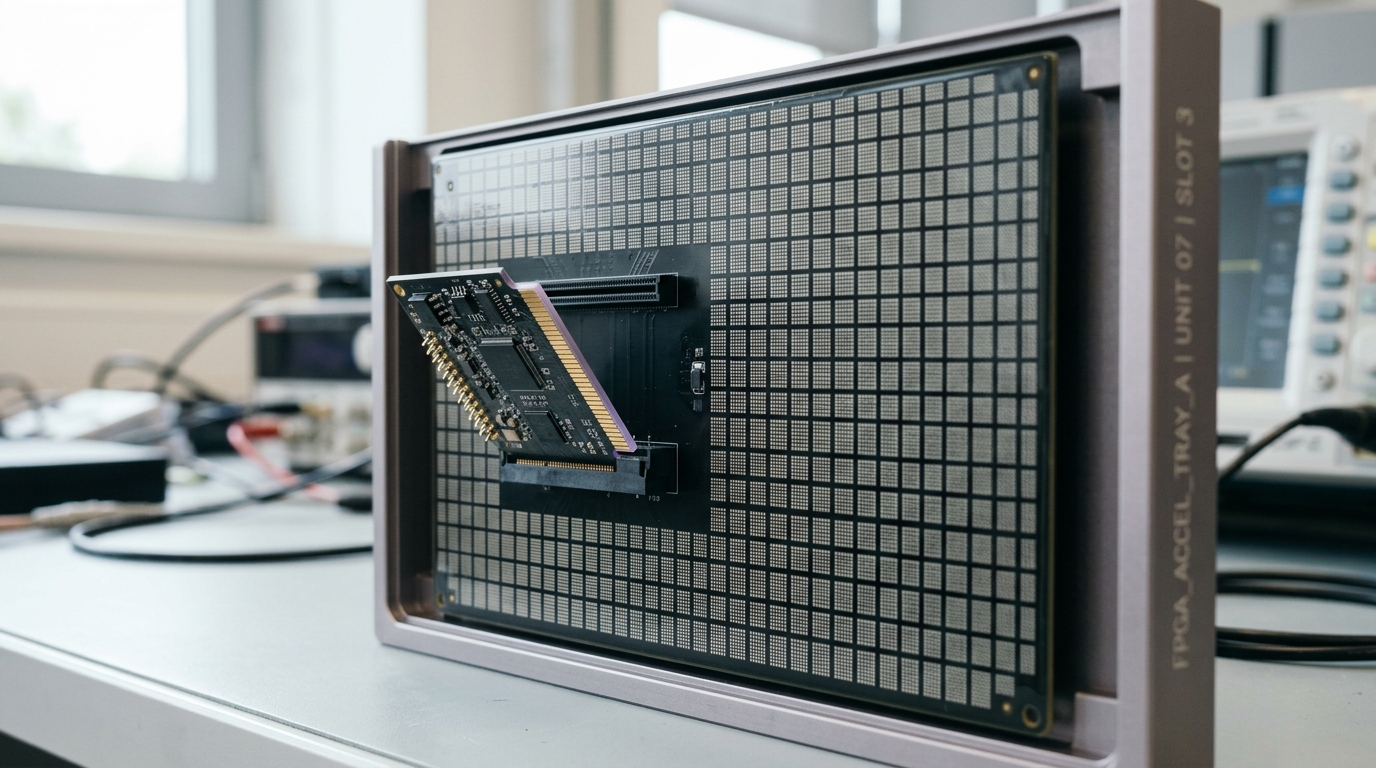
FPGA-based systems make the same compiler-first bet on commodity reconfigurable fabric. Microsoft’s Project Brainwave describes “a high-performance, precision-adaptable FPGA soft processor” reaching “up to 39.5 TFLOPs of effective performance at Batch 1 on a state-of-the-art Intel Stratix 10 FPGA,” built to serve pre-trained models “with high efficiencies at low batch sizes” in production search and cloud services [5]. The batch-size-one framing recurs across this family for a reason: it is exactly where a GPU’s scheduler has nothing to overlap and a statically planned pipeline has nothing to wait for.
Not every architecture here fixes the spatial layout ahead of time; some fix only the communication pattern. Graphcore’s Intelligence Processing Unit is architecturally closer to a many-core MIMD processor than to a CGRA or streaming array: an independent microbenchmarking study by researchers at Citadel, who report early hardware access from Graphcore but no funding relationship or employment there, documents 1,216 independent tiles per IPU, each “one computing core plus 256 KiB of local memory,” offering “true MIMD (Multiple Instruction, Multiple Data) parallelism” with “distributed, local memory as its only form of memory on the device” — a deliberate contrast with SIMT, since the IPU, the same researchers write, “unlike other massively parallel architectures (e.g., the GPU), adapts well to fine-grained, irregular computation that exhibits irregular data accesses” [6]. Tiles communicate in bulk-synchronous phases across an on-chip interconnect the authors call “the exchange,” rather than through the fully static instruction stream Groq’s compiler produces — a genuinely different point on the static-versus-dynamic spectrum, not a restatement of it.
The memory-side answer: near- and in-memory compute
The fourth family does not try to make feeding the arithmetic unit faster or more predictable. It asks whether the arithmetic unit needs to be a separate thing at all. Mutlu and colleagues frame the motivation directly: in a conventional system, “to perform any operation on data that resides in main memory, the memory controller must first issue a series of commands to the DRAM modules… This process of moving data from the DRAM to the CPU incurs a long latency, and consumes a significant amount of energy,” made worse by the fact that much of the data brought into cache is never reused [7]. Their survey describes two branches of response: simple bulk operations performed directly inside DRAM by exploiting its analog electrical properties at low cost, and genuine logic placed in the layer of a 3D-stacked memory die to accelerate data-intensive kernels near where the data already lives [7].
The clearest commercial instance is UPMEM’s processing-in-memory hardware, which places general-purpose in-order cores called DRAM Processing Units directly on standard DDR4 modules — eight DPUs per chip, each with exclusive access to its own 64 MB DRAM bank, a 24 KB instruction memory and a 64 KB scratchpad, communicating with a host CPU that issues code and data and later retrieves results [8]. A comprehensive independent characterisation of that hardware, built around a purpose-designed sixteen-workload benchmark suite the authors call PrIM and explicitly selected using the roofline model to identify genuinely memory-bound problems, evaluated real UPMEM systems of 640 and 2,556 DPUs against CPU and GPU counterparts [8]. The same authors summarise why the underlying bet is plausible at all: separate measurement studies they cite found data movement responsible for 35% of total system energy in 2013, 40% in 2014, and 62% in 2018 across scientific, consumer and mobile workloads respectively — a share that has been rising as arithmetic has gotten cheaper relative to moving operands to it [8].
Near-memory compute’s central limitation sits in the same architecture description that makes its promise clear. Because each DPU’s exclusive high-bandwidth path runs only to its own memory bank, there is, in the authors’ words, “no support for direct inter-DPU communication”; anything that must move between DPUs is retrieved and re-copied by the host CPU [8]. The design that eliminates the memory-to-compute distance for a single core’s own data reintroduces almost the entire cost of that movement at the far more expensive host round trip the moment two cores need to talk. A workload with abundant per-core locality and little cross-core communication is close to the architecture’s best case; one built from frequent reductions or all-to-all exchange is close to its worst, for reasons that follow from the physical layout rather than any deficiency in the individual DPU.
Utilization is a product of two different things, not one
It is tempting to compare these four families by a single number — peak operations per second, or operations per watt — and the rest of this article explains why that number, alone, is close to meaningless. A more useful decomposition separates what a device can theoretically do from what a piece of software actually gets it to do, and splits that gap into two distinct causes:
Here
This decomposition is also why a device’s peak number and its delivered number can diverge by an order of magnitude depending entirely on software maturity, with no change to the silicon — and why comparing two architectures’ peak numbers, without separately accounting for how mature each compiler is at extracting
What compiler maturity actually buys, and costs
The practical consequence of pushing utilization into the compiler is that a chip’s real-world value is inseparable from the maturity of its software stack, and that maturity takes years and is not portable between architecture families. Sara Hooker’s widely cited argument names the dynamic directly: “a research idea wins because it is suited to the available software and hardware and not because the idea is superior to alternative research directions,” and she warns that as hardware becomes more specialised this effect gets stronger, because a promising architecture with an immature toolchain can lose to a worse architecture with a decade of compiler investment behind it [9].
That argument explains a pattern visible across every family here, each sitting at a different point on the same tradeoff between how much engineering effort a chip demands from its software stack and how much of that effort the hardware’s own regularity can substitute for. The GPU’s position owes as much to a compiler and library ecosystem built over more than a decade — one that lets almost any idea be expressed and reasonably well scheduled without hand-tuning — as to the hardware itself. A systolic array’s compiler has a narrower, more tractable job: mostly tiling dense matrix multiplications well, with little recourse when a workload does not decompose that way. A statically scheduled dataflow chip asks the most of any family here, since there is no reactive hardware left to compensate for a suboptimal schedule [3]. Near-memory compute asks the least of a general compiler and the most of a programmer, since exploiting the architecture well means restructuring an algorithm around per-DPU locality by hand rather than trusting a mature automatic mapper [8].
Precision exposure differs by family, not just by generation
Numerical precision is often discussed as a single axis every architecture moves along together, but the four families expose precision control quite differently. The original TPU’s matrix unit was built natively around 8-bit multiply-accumulate operations rather than offering 8-bit as one option among several [1], buying density at the cost of flexibility later designs had to add back deliberately. Project Brainwave’s authors describe their FPGA soft processor specifically as “precision-adaptable,” treating reconfigurable numeric format as a first-class feature of building on reconfigurable fabric rather than fixed silicon [5]. A modern GPU exposes a growing menu of formats side by side in one silicon generation, letting a single chip serve workloads with different range-versus-precision needs without swapping hardware. Near-memory compute sits at the opposite end from the reconfigurable fabric: UPMEM’s DRAM Processing Units are general-purpose in-order cores with a fixed local instruction set rather than dedicated floating-point matrix engines [8], so the numerical repertoire available to a program is set by the processor’s basic instruction set rather than a configurable arithmetic pipeline — a constraint that shapes which workloads are realistic candidates as much as bandwidth does.
Why “TOPS per watt” cannot rank these families
Power efficiency is the number buyers most want reduced to a single ranking, and the least safe to reduce that way, for reasons beyond the usual caution about peak-versus-achieved throughput. The four families are typically measured under different conditions — die-only power versus board power versus rack power, different process nodes, precisions and batch sizes, and workloads chosen because they flatter the architecture being announced. The TPU paper’s own 30-to-80-times performance-per-watt figure against 2015-era CPU and GPU hardware, cited earlier, shows exactly how wide that gap can look under one company’s own chosen comparison [1], and exactly why it cannot be extended to a different company’s current hardware.
The industry’s own benchmark body concedes the same point structurally rather than as a caveat. MLCommons’ MLPerf training rules define a Closed division that “requires using the same preprocessing, model, training method, and quality target as the reference implementation” so that submissions stay comparable, and a separate Open division that explicitly “allows using arbitrary training data, preprocessing, model, and/or training method” for participants showing off architecture-specific advantages the Closed division’s standardisation would hide [12]. That split is itself evidence for the argument here: the organisation built specifically to make cross-vendor AI hardware comparisons possible has concluded that a single unconstrained number is not trustworthy, and built an entire second division to house the results that are not.
The honest version of a power-efficiency comparison is conditional rather than a league table: at matched precision, batch size and measurement boundary, which architecture delivers more useful work per watt on a specific workload — and that answer differs, and is allowed to differ, by workload.
Where the real disagreements are
Three disagreements in this space are genuine and unresolved, not manufactured for balance.
The first is whether statically scheduled dataflow and reconfigurable architectures are a durable third path or a niche squeezed between the GPU’s software gravity and the systolic ASIC’s efficiency ceiling. The technical case for the middle path is real: Groq’s and Plasticine’s authors both demonstrate, in peer-reviewed venues, that eliminating runtime scheduling logic recovers real efficiency without giving up reconfigurability for more than one workload shape [3] [4]. The skeptical case is commercial rather than technical: a compiler mature enough to make that promise pay off across a wide range of workloads is an enormous, multi-year undertaking, and several companies in this space, Groq included, now sell access to their hardware primarily as a hosted inference service rather than as a chip customers program directly [3] — a business choice that may reflect the size of that compiler burden as much as the architecture’s technical ceiling. Nothing in the public record settles which explanation dominates, and this article does not either.
The second is whether near-memory compute is a genuine fourth path out of the memory wall or a narrow-workload curiosity. The case for is architectural and well evidenced: data movement’s share of system energy is large and growing, and DPU-local processing removes the most expensive hop in that movement entirely for workloads with strong per-core locality [7] [8]. The case against, from the same independent researchers, is equally well evidenced: the moment a workload needs meaningful communication between processing units, that traffic is forced through the host CPU, reintroducing much of the cost the architecture was built to remove [8]. Both claims are true simultaneously; they describe different workloads.
The third is whether the GPU-versus-ASIC distinction is dissolving or hardening. One view, supported by NVIDIA’s own generational disclosures, is that GPUs are absorbing enough systolic-style matrix hardware and data-movement engines that the practical gap between “a GPU” and “a matrix ASIC with a general-purpose core attached” is shrinking each generation [11]. The opposing view, grounded in Kung’s original argument, is that a chip which never carries instruction issue or scheduling logic inside its compute array keeps a structural advantage no amount of added matrix hardware on a general-purpose core can fully close, because that core still pays the area and power cost of generality every cycle whether or not a given kernel needs it [2]. Resolving this would need a matched-precision, matched-workload, matched-measurement-boundary comparison that, as the previous section argues, does not currently exist in a form fair to cite.
Reading rules for anyone comparing these chips
A short discipline follows from all of the above, regardless of which family a given evaluation favours.
Ask what is fixed and what is scheduled, and when. Whether a schedule is fixed at design time, fixed at compile time, or decided at runtime predicts more about a device’s behaviour than its headline throughput number does.
Separate
Never carry a vendor’s self-comparison across companies or years. Every dated, single-vendor performance-per-watt or speedup figure here, including the TPU’s own reported numbers, describes that vendor’s progress against its own prior hardware and nothing else.
Treat workload shape as the actual independent variable. “Which architecture is better” is underspecified until batch size, sparsity, precision and communication pattern are pinned down, because the four families’ relative standing changes with each.
Predictions, with what would falsify them
These are forecasts, clearly separated from the sourced analysis above. Horizon: 15 August 2030.
One. GPUs will keep absorbing systolic-style matrix hardware and data-movement engines each generation, narrowing but not eliminating the efficiency gap to purpose-built matrix ASICs on dense, well-shaped workloads. Disconfirmed if a major vendor’s flagship part ships a generation where the general-purpose SIMT core, rather than the matrix engine, gets the larger area and power allocation.
Two. Statically scheduled dataflow and reconfigurable architectures will remain viable mainly as vertically integrated inference services rather than chips broadly programmed by third-party compiler teams, because the compiler investment does not amortise well across independent customers. Disconfirmed if two or more software organisations unaffiliated with the hardware vendor ship production compilers for the same statically scheduled architecture within the horizon.
Three. Processing-in-memory will stay confined to a narrow, well-characterised set of high-locality, low-reuse workloads — the PrIM suite’s target class — rather than becoming general-purpose, because the inter-unit communication limitation is architectural, not a tooling gap. Disconfirmed if a commercial PIM system ships native, low-latency inter-processing-unit communication that does not route through a host CPU.
Four. Cross-vendor accelerator comparisons published without matched precision, batch size and measurement boundary will become less credible and more frequently challenged, following the trajectory MLPerf’s Closed/Open split already set for training benchmarks. Disconfirmed if single unconditioned throughput or efficiency figures remain the dominant form of accelerator comparison in mainstream reporting through the horizon with no comparable pushback.
What to take away
Four architectures, four answers to one question: who decides the schedule, and when. The GPU keeps that decision in a runtime scheduler and pays for the privilege in silicon it does not always need. The systolic array removes the decision by fixing it into the geometry of the array, and pays in rigidity. Dataflow and reconfigurable architectures move the decision into the compiler, trading a large upfront software burden for hardware that can, in principle, be redrawn for the next workload. Near-memory compute makes the question disappear for a narrow but real class of problems by putting the arithmetic where the data already is, at the cost of everything that needs to talk across processing units.
None of that supports a ranking, and any comparison that produces one without naming a workload, a precision, a batch size and a measurement boundary has quietly chosen those four things for you. The question worth asking of any accelerator claim is not “is this faster,” but “faster than what, doing what, measured how, and against which of that company’s own prior parts” — and if any of those four is missing, the number in front of you is marketing wearing an engineering paper’s clothes.