Why this needs to be five separate claims, not one forecast
“Memory will keep getting faster” is not a prediction; it is a truism with no way to be wrong. This article exists because the interesting questions about AI memory systems by 2035 are not truisms. Will HBM bandwidth per stack keep doubling on roughly its historical cadence, or does the stacking approach run into a mechanical or thermal ceiling first? Does CXL-pooled memory become a default fitting in AI racks, or does it stay a specialist’s tool for a narrow set of workloads? Does processing-in-memory — a claim the industry has been making in press releases since at least 2021 — finally cross into production, or does it remain a decade-long pattern of demonstrations that never quite ship? Does the growth of the key-value cache force a structural change in how attention itself is computed, or does hardware simply absorb the growth? And is there a memory technology, not yet in a bandwidth-critical role today, that could break all of the above trends at once?
Each of those is answered here as a scenario: a claim with a stated horizon, the assumptions it depends on, the observable indicators that would move a reader’s confidence one way or the other, and — critically — the specific observation that would prove it wrong. Facts, vendor assertions and analysis are kept visibly distinct from one another throughout, because the two most common failures in memory-systems forecasting are treating a marketing claim as a measurement, and treating an extrapolated line as a law of nature.
Where the standard actually stands
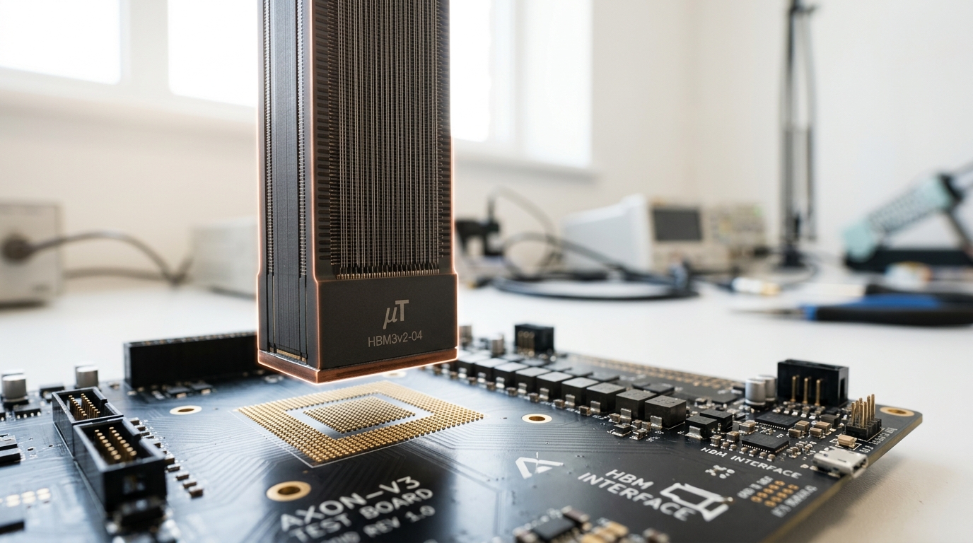
Start with what is verifiably true today, because every scenario below is a departure from this baseline. JEDEC — the standards body whose members include the DRAM manufacturers, the accelerator vendors and the packaging houses that actually build this hardware — published the JESD238 HBM3 standard in January 2022. It specifies data rates of up to 6.4 gigabits per second per pin, which across HBM3’s interface works out to roughly 819 gigabytes per second per stack; 16 independent channels, doubled to an effective 32 via two pseudo-channels per channel; and stack heights of 4-high, 8-high and 12-high, with capacities from 4 gigabytes up to 64 gigabytes per stack [1]. JEDEC then finalized JESD270-4, the HBM4 standard, in April 2025. HBM4 doubles the interface to 2,048 bits and moves to 8 gigabits per second per pin, for a stated bandwidth of up to 2 terabytes per second per stack; it doubles the channel count again, to 32 real channels each still split into two pseudo-channels; it extends stack heights to 16-high with 24- or 32-gigabit dies, for a maximum single-stack capacity of 64 gigabytes; and JEDEC set a relaxed nominal package thickness of 775 micrometers specifically to accommodate the taller 12-high and 16-high configurations [2]. That last detail is a fact worth sitting with: the standards body is already negotiating a mechanical tolerance to keep stacking taller, which is direct evidence that the stacking approach is approaching, not indifferent to, a physical constraint.
Beyond HBM4, the record is vendor roadmap rather than ratified standard. SK hynix has stated it expects to begin developing HBM5 and HBM5E, along with a custom HBM5 variant, in the 2029–2031 window, as reported from the company’s own roadmap disclosure — a vendor assertion about intent, not a JEDEC specification, and one that comes with no published bandwidth target [3]. Treat it accordingly: it tells us where one manufacturer says it is aiming, not what the industry has agreed to build.
A scenario for the bandwidth trajectory to 2035
With two verified anchor points — HBM3 in 2022 at roughly 0.82 terabytes per second per stack, HBM4 in 2025 at up to 2.0 terabytes per second per stack [1, 2] — it is possible to build an explicit, falsifiable trajectory rather than a vague “bandwidth will keep rising.” Model the growth as a simple exponential in calendar time,
where
Extrapolated naively, ten more years at that doubling time — roughly 4.3 further doublings — would put per-stack bandwidth near 39 terabytes per second by 2035. That number should not be believed as stated, and the reason it should not be believed is itself the analytically interesting point. A two-point fit is not a trend; it is a line drawn through the only two data JEDEC has actually ratified. And it runs well ahead of the general DRAM-and-interconnect bandwidth scaling documented across two decades of hardware by Gholami and colleagues, who report peak server FLOPS scaling at roughly 3.0 times every two years against DRAM bandwidth scaling at only 1.6 times and interconnect bandwidth at 1.4 times over the same interval [13]. Apply that slower, broader-based 1.6×-per-two-years rate to the same 2025 starting point instead, and 2035 bandwidth lands closer to 21 terabytes per second per stack — almost half the naive HBM-specific extrapolation.
The gap between those two numbers is not noise; it is a structural question with a name. HBM’s per-stack bandwidth has, so far, grown faster than generic DRAM bandwidth because each generation adds more than one lever at once — more channels, more pins, more layers, and a higher signaling rate together — while the “1.6× per two years” figure describes a single memory technology’s bit-rate scaling in isolation. Whether HBM can keep pulling multiple levers simultaneously through the late 2020s, or whether it converges toward the generic DRAM rate as those levers run out — thermal density per stack, TSV count per die, and the package-thickness tolerance JEDEC has already had to relax once — is exactly the open question a 2035 forecast has to take a position on rather than paper over.
Scenario. The HBM-specific rate persists through the 2020s because packaging (hybrid bonding, taller stacks) and channel-count growth continue to substitute for raw per-pin signaling gains, then converges toward the generic DRAM-bandwidth rate once stack height and package thickness stop moving. This scenario, its assumption, and its disconfirmation condition are stated formally as Prediction One below.
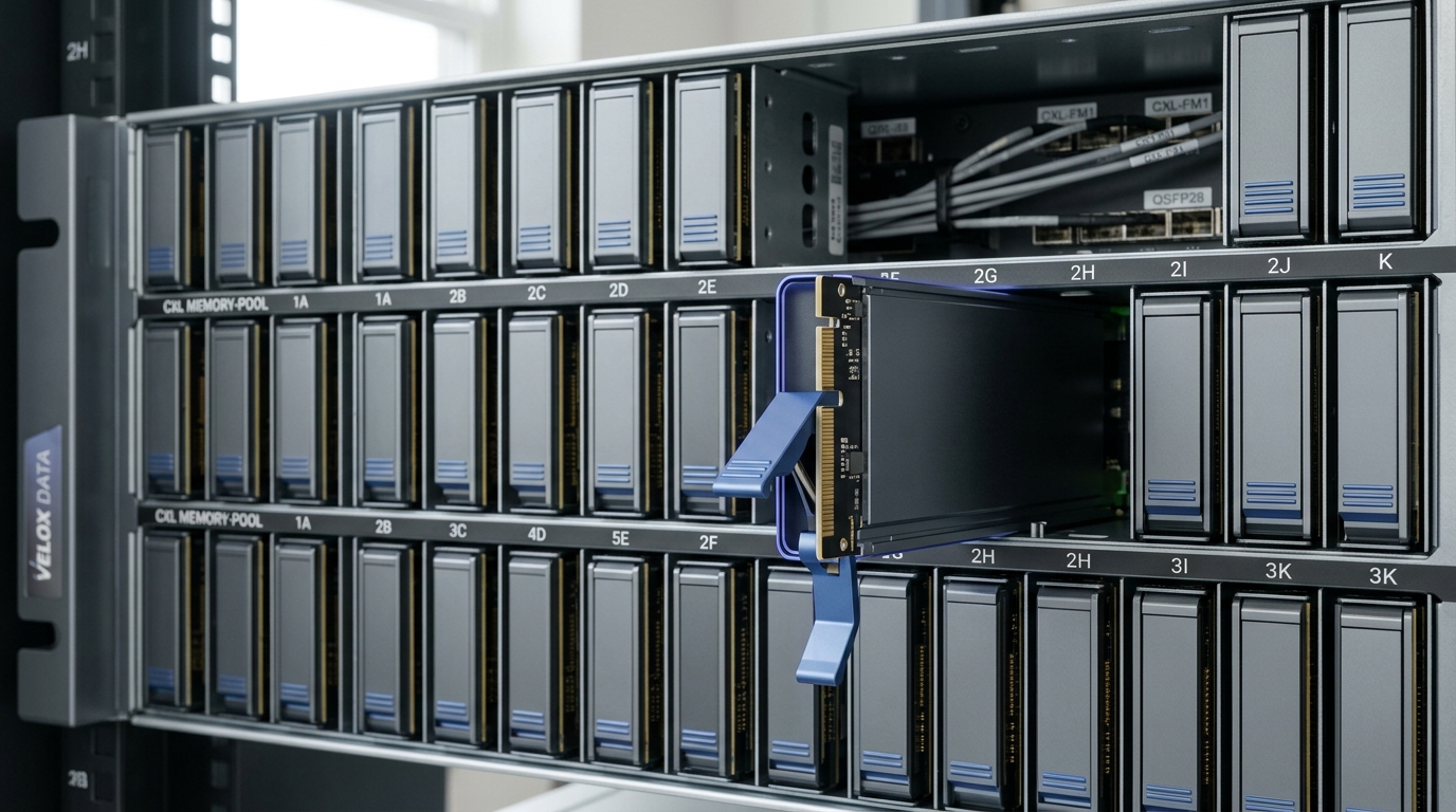
CXL: mainstream fabric or permanent niche
Compute Express Link is where the disagreement among informed parties is sharpest, and it is worth presenting that disagreement rather than resolving it, because none of the three positions below is obviously wrong given what is publicly known.
Fact. The CXL Consortium’s memory-pooling capability is not new. CXL 2.0 introduced pooling in 2020; CXL 3.0 added true multi-host coherent sharing; and the most recent ratified specification, CXL 3.2, released in December 2024, added a Hot-Page Monitoring Unit for memory tiering, Post Package Repair enhancements, expanded security via the Trusted Security Protocol, and remained fully backward compatible — in other words, it is a management-and-reliability release layered on pooling functionality the standard already had, not a new pooling capability in itself [4].
Vendor assertion. In March 2026, Marvell announced its Structera S 30260 CXL switch, claiming aggregate bandwidth up to 4 terabytes per second, sub-microsecond access to shared memory, and marketing itself as “the first true CXL switching solution purpose-built for AI.” A Marvell vice president is quoted stating that “breaking through the AI memory wall requires a fundamental architectural change” [6]. That is a vendor’s characterization of its own product’s importance, sampling to customers in the third quarter of 2026 according to the same release — a real, dated commercial commitment, but not independent evidence that pooling delivers the stated benefit at scale.
Academic measurement. The most careful independent evaluation of CXL pooling’s actual payoff is Pond, an ASPLOS 2023 Distinguished Paper Award winner built and evaluated against real cloud production traces. Its authors report that CXL-based pooling reduces DRAM costs by roughly 7 percent while keeping performance within 1 to 5 percent of same-NUMA-node allocation — a real, positive, but modest gain, not a transformation. They also found that pooling across just 8 to 16 sockets captures most of the achievable benefit, which argues for small, low-latency pools rather than large fabric-wide ones [7]. That is the single most sober number available in this section, and it sits well below the ambition implied by vendor marketing.
Analyst caution, separately sourced. A 2025 infrastructure-planning assessment characterizes CXL adoption as early-stage: current deployments are described as still in a “production evaluation” phase for CXL 2.0, with CXL 3.0/3.1 pegged for “early adoption for AI” only in late 2026, citing ABI Research’s expectation that CXL 3.0/3.1 solutions will not have sufficient software support for broad commercial adoption until 2027. The same assessment notes CXL 4.0’s headline bandwidth — 512 gigabytes per second per x16 port, up to 1.5 terabytes per second bundled — sits at roughly 30 percent of contemporary GPU memory bandwidth, and states plainly that “CXL software support remains early-stage,” with Linux kernel support present but application-level optimization still lacking [5].
Characterizing the disagreement. These three sources are not measuring the same thing, which is part of why they read as contradictory. Marvell is asserting product importance ahead of shipment. Pond is measuring realized savings in one production workload class (cloud VM memory allocation) years before the newest switch silicon existed. The infrastructure-planning assessment is describing software and ecosystem maturity, which lags hardware capability by design in any interconnect standard. None of the three is dishonest; they simply answer “is CXL pooling mainstream” from three different vantage points — commercial ambition, realized benefit, and deployment readiness — and a forecast that picks one and ignores the other two is not more confident, just less complete.
Processing-in-memory: a decade of demonstrations
The pattern in processing-in-memory (PIM) is unusually clean, because it has been running long enough to show its own shape.
Vendor assertion, 2021. Samsung announced HBM-PIM — an HBM2-based device with a DRAM-optimized SIMD engine placed inside each memory bank — claiming, in its own press materials, more than double the system performance and a reduction in energy consumption of over 70 percent when applied to its existing Aquabolt HBM2 product, and stating explicitly that the approach required no hardware or software changes to the host processor [8]. That is a striking claim, presented by the company that made the part, about the company’s own part.
Device measurement, independent. The most thorough independent characterization of a real, commercially available PIM architecture is not Samsung’s HBM-PIM but UPMEM’s DRAM Processing Unit design, benchmarked by Gómez-Luna and colleagues across systems with 640 and 2,556 processing units. Their study built the sixteen-workload PrIM benchmark suite spanning linear algebra, databases, graph processing, neural networks and bioinformatics specifically because the architecture’s real behavior — which workloads it actually helps, and by how much — could not be established from vendor claims or simulation alone; it required running real memory-bound kernels on real silicon [10]. The paper’s existence is itself informative: after years of PIM announcements, an independent, hardware-based characterization was still novel enough to be a notable contribution in 2021.
Vendor demonstration, current. SK hynix showed an updated version of its own PIM line, marketed as AiM and packaged into accelerator cards called AiMX, at the AI Infra Summit in September 2025, running a Supermicro server fitted with two Nvidia H100 GPUs alongside four AiMX cards. The company’s claims — that the combination lets a server “simultaneously process more user requests and longer input prompts” than a GPU-only system, at lower operating cost, with stable behavior for long token generation in reasoning models — are, again, the vendor’s own characterization of its own demonstration, not a third-party benchmark [9].
Analysis. Line these three up and a pattern appears that a single snapshot would miss: a 2021 vendor claim of dramatic, no-integration-cost gains; an independent 2021 measurement effort whose main contribution was simply establishing ground truth on real hardware, because ground truth did not yet reliably exist; and a 2025 vendor demonstration that is still a demonstration — a booth at a conference, paired with mainstream GPUs rather than replacing them — four years later. Memory-Centric Computing, a 2025 survey by Mutlu and colleagues, argues the underlying case for PIM has only strengthened: memory now dominates a system’s energy, performance bottlenecks and cost, and enabling computation inside memory chips can improve efficiency by orders of magnitude on the workloads it fits [11]. That argument, made by researchers with a long track record studying this exact architecture, is a reason to take PIM seriously as a direction — it is not, by itself, evidence that the direction has become a production default. Four years between vendor claim and vendor claim, with no widely reported hyperscale production deployment in between, is itself data about the pace of this transition.
KV-cache pressure and the shape of future architecture
Fact. The memory a transformer must hold for one in-flight generation — its key-value cache — grows linearly in exactly the variables that make serving expensive: sequence length and batch size. For a model with
bytes, the leading factor of two accounting for keys and values together. That equation is worth writing out because it exposes the one real lever every mitigation below actually pulls: none of them escapes linear growth in
Peer-reviewed evidence, three different levers. DeepSeek-V2 replaces full multi-head keys and values with a low-rank latent projection — reducing
Analysis. This is where the article’s four questions connect. If algorithmic compression of the kind above keeps outpacing context-length and concurrent-batch growth, then KV-cache pressure is absorbed in software, and the HBM bandwidth trajectory only has to keep up with weights traffic and a shrinking cache — nudging the scenario in the previous section toward its slower, generic-DRAM-rate branch. If context lengths and batch sizes instead grow faster than compression techniques can shrink the other factors — which is plausible, since agentic and long-horizon workloads push
What could force a discontinuity
Every scenario above assumes DRAM-based HBM remains the working memory sitting closest to the compute, with CXL and PIM as additions around it rather than replacements of it. The most credible source of a discontinuity would be a memory technology that is not DRAM crossing into that specific role.
Fact, from a 2024 peer-reviewed review. Emerging non-volatile memory technologies — magnetic (MRAM), resistive (ReRAM), phase-change (PCM) and ferroelectric (FRAM) — are, per Hellenbrand and colleagues’ review in MRS Communications, at genuinely different stages of maturity. MRAM and ReRAM are the most advanced: Samsung shipped embedded STT-MRAM in mass production at 28 nanometers in 2019, and TSMC offers both STT-MRAM and ReRAM in production today, with TSMC having demonstrated a 12-nanometer FinFET ReRAM bit cell as small as 0.0249 square micrometers. PCM and FRAM, by contrast, remain — in the review’s own words — “less available as commercially available products.” The authors’ own framing of where this is headed is precise and worth quoting directly: these technologies already “have a strong foothold in the semiconductor industry with the main target of replacing embedded flash memory, and soon possibly DRAM and SRAM” [12].
Analysis. Read that sentence carefully rather than optimistically. The stated target is replacing embedded flash now, with DRAM and SRAM named as a “soon possibly” — a hedge from researchers who study these devices for a living, not a timeline. None of the four technologies surveyed is reported as production-ready in a bandwidth-critical, HBM-adjacent role today. That is the honest state of the evidence: emerging memory is real, shipping, and improving, but it is shipping into different sockets than the one this article is asking about. A genuine discontinuity in the sense this article means — a non-DRAM technology displacing HBM as an accelerator’s primary high-bandwidth working memory — has not happened yet and is not clearly imminent from any single public data point available today.
Scenario. The likeliest near-term discontinuity is therefore not a wholesale replacement but a boundary shift: an eNVM technology first displacing part of the capacity tier that CXL currently targets (cold or warm KV-cache and model-weight offload, where ReRAM’s or MRAM’s non-volatility and density are the selling point) before it ever approaches HBM’s bandwidth-critical role. That would not falsify the HBM trajectory scenario above; it would instead compete directly with, and could substantially undercut, the CXL-pooling scenario, since composable capacity is exactly the market both are aiming at.
Predictions, with the observations that would falsify them
These five claims follow from the sourced material above; the reasoning for each is developed in its own section. Horizon dates are chosen individually because HBM’s standards cadence, CXL’s software maturation, and PIM’s commercial history do not move at the same speed.
One — HBM bandwidth trajectory. Horizon: 2032. Assumption: JEDEC’s demonstrated willingness to relax mechanical tolerances (the 775-micrometer package thickness for taller HBM4 stacks) continues to substitute for pure per-pin signaling gains. Indicator: whether JEDEC ratifies an HBM5 standard on a cadence close to HBM3→HBM4’s three years, and what per-stack bandwidth it specifies. Disconfirmed if no successor standard to HBM4E is ratified by 2030, or if the ratified per-stack bandwidth growth has decelerated to the roughly 1.6×-per-two-years generic DRAM-bandwidth rate documented by Gholami and colleagues [13] rather than the faster HBM-specific rate implied by JESD238 and JESD270-4 [1, 2].
Two — CXL pooling, mainstream or niche. Horizon: 2029. Assumption: the three-way disagreement described above (vendor ambition, Pond’s measured 7 percent saving, and analysts’ 2027 software-maturity estimate) persists into deployment data rather than resolving early. Indicator: the share of new hyperscale AI server designs shipping CXL-attached pooled memory by default, as disclosed in vendor architecture briefings or analyst fleet surveys. Disconfirmed as mainstream if, by 2029, CXL pooling remains confined to specialized capacity-offload roles in a minority of deployments; disconfirmed as permanently niche if, by the same date, a majority of new designs from at least two of the three largest hyperscalers ship it by default [4, 5, 7].
Three — processing-in-memory reaches production. Horizon: 2030. Assumption: crossing from demonstration to production requires both a workload with an unambiguous bandwidth-bound bottleneck and a standardized software stack, not a bespoke vendor SDK. Indicator: a PIM or near-memory-compute capability appearing inside a JEDEC-standardized memory module, or a hyperscaler publicly disclosing PIM in production serving, rather than at a conference booth. Disconfirmed if, by 2030 — nine years after Samsung’s HBM-PIM announcement and five after SK hynix’s AiMX demonstrations — PIM remains confined to research benchmarks and vendor showcases without a disclosed production deployment [8, 10, 9].
Four — KV-cache pressure forces architectural change. Horizon: 2030. Assumption: context length and concurrent-batch demand continue to grow faster than per-accelerator memory capacity. Indicator: whether latent-compression or learned-eviction attention variants comparable to multi-head latent attention, attention sinks, or heavy-hitter eviction become default choices across mainstream frontier model releases, not just the labs that introduced them. Disconfirmed if, by 2030, mainstream architectures still standardize on uncompressed multi-head or plain grouped-query attention, in which case hardware bandwidth scaling will have had to absorb the growth in
Five — no discontinuity in the accelerator’s primary working memory. Horizon: 2035. Assumption: no eNVM technology — MRAM, ReRAM, PCM or FRAM — closes the multi-order-of-magnitude bandwidth and endurance gap against DRAM-based HBM in a decade. Indicator: an eNVM technology entering production specifically in a bandwidth-critical, HBM-adjacent role, as opposed to embedded-flash replacement or CXL-tier capacity offload. Disconfirmed if, by 2035, a non-DRAM memory technology ships in volume as the primary working memory of a mainstream AI accelerator, replacing HBM in that specific role — a claim no source reviewed for this article currently supports, but one the Hellenbrand review’s own “soon possibly DRAM and SRAM” hedge leaves explicitly open [12].
What to take away
Four of these five questions are, on the public record, genuinely undecided, and the honest position is to say so with a date attached rather than to guess with confidence attached. The HBM trajectory has two defensible extrapolations three years apart in doubling time and roughly a factor of two apart in the resulting 2035 number, depending on an assumption about which physical levers keep moving. CXL pooling has a real, modest, independently measured benefit sitting well below its vendor marketing and well ahead of its software maturity. Processing-in-memory has now produced two vendor-claimed breakthroughs four years apart with no confirmed production deployment between them. KV-cache compression is winning specific, large, peer-reviewed victories against specific terms in a linear equation that none of them actually escapes. And the memory technology most often invoked as a future discontinuity is, by its own most careful reviewers’ account, currently aimed at a different socket entirely.
None of that is a failure of the evidence. It is what the evidence, read honestly and dated correctly, actually says in 2026. A forecast that resolved all five questions confidently today would be manufacturing certainty the sources do not contain. The five predictions above do the opposite: each names the exact observation that would prove it wrong, which is the only property that separates a prediction from an opinion.