What actually crosses each boundary
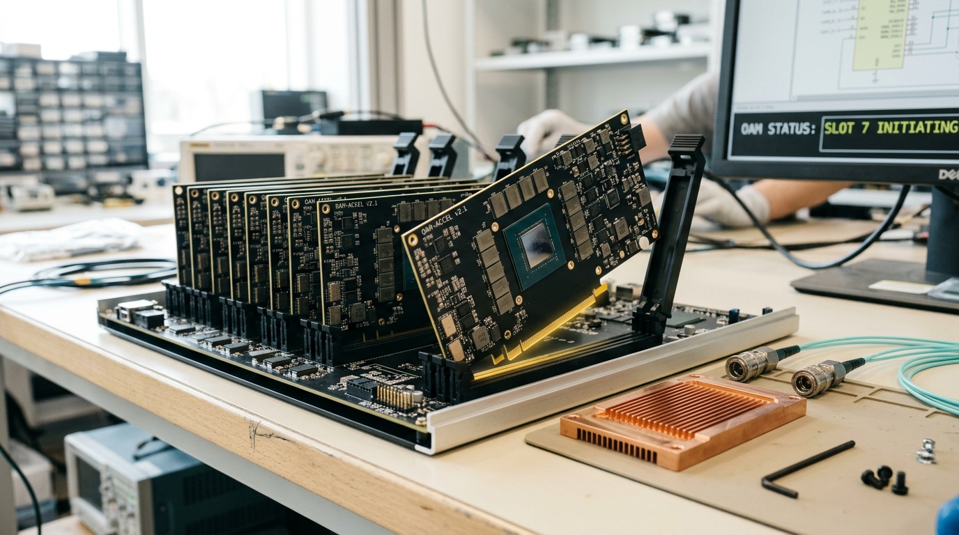
An earlier piece in this series surveyed the memory hierarchy as a set of tiers at increasing distance from the arithmetic units, and showed why a fast kernel is fast mainly because of what it never reads. That is the right level for understanding why data movement dominates. It is the wrong level for understanding how a byte actually gets from a capacitor to a register. This article stays at that second level throughout: not the shape of the hierarchy, but the physical and protocol mechanisms that move a bit across each boundary in it — the cell, the stack, the external link, and the cache that keeps growing underneath a running model.
Four mechanisms carry the argument. A memory cell is a trade between speed and density made once, in silicon, and it cannot be renegotiated by software. A high-bandwidth memory (HBM) stack turns that trade into bulk bandwidth by running many narrow, slow paths in parallel through a forest of vertical interconnects. The Compute Express Link (CXL) protocol lets memory live outside the accelerator package while a program still addresses it as ordinary memory, at the cost of a real, measurable latency tax. And a large language model’s key-value (KV) cache is the clearest case in current computing of a data structure whose size is not a design choice but an arithmetic consequence of how long a conversation has run. Each of these is verifiable against a published specification, a peer-reviewed measurement, or a vendor’s own device paper, and each is cited as such below.
The cell decides the ceiling
Every tier in the hierarchy ultimately rests on one of two ways to hold a bit in silicon, and the choice between them is made at the transistor level, long before an architect gets to decide anything about caches or buses.
Static RAM (SRAM) stores a bit as the state of a cross-coupled pair of inverters — commonly six transistors per cell — which holds its value as long as the cell is powered and can be read or written in roughly the time it takes a transistor to switch. Dynamic RAM (DRAM) stores a bit instead as charge on a tiny capacitor accessed through a single transistor. That one-transistor-one-capacitor cell is far smaller than an SRAM cell in the same process, which is why a DRAM array packs many more bits into the same silicon area — and it is the reason DRAM, not SRAM, is what sits in a high-bandwidth memory stack or a CXL memory expansion module, where capacity is the point.
The capacitor is also DRAM’s central liability. It leaks. A DRAM cell’s charge decays over time, so every row in every DRAM array must be read and rewritten — refreshed — before it decays past the point where a sense amplifier can reliably tell a one from a zero. Refresh is not free: while a row is being refreshed it cannot service a normal read or write, and the fraction of time spent refreshing grows as chips pack in more rows to refresh within the same retention window. Liu, Jaiyen, Veras and Mutlu’s RAIDR work — revisited in a retrospective marking fifty years of the International Symposium on Computer Architecture — addressed this directly by observing that retention time varies substantially from row to row on real DRAM chips, and that grouping rows into bins by their measured minimum retention time, tracked cheaply in Bloom filters, and refreshing each bin only as often as its worst row actually requires, cuts unnecessary refresh operations sharply, with the benefit growing as chip capacity grows [14]. That single mechanism illustrates the deeper point: DRAM’s density advantage is bought with an ongoing maintenance tax that SRAM simply does not pay, and every DRAM-based tier in an AI system — HBM included — inherits that tax whether or not the software running on it is aware of it.
Registers and on-die SRAM cache sit above this line because they are built from the fast, non-leaking cell; HBM, CXL-attached memory, and system DRAM sit below it because they are built from the dense, leaking one. Nothing above this paragraph is negotiable at the software level. Everything that follows is about how engineers have built around that one fixed trade to get bulk bandwidth out of the slower, denser cell anyway.
Stacking the DRAM: TSVs, interposers, and the width trick
A single DRAM die, read at a comfortable per-pin data rate, cannot come close to feeding a modern accelerator. HBM’s answer is not to make DRAM faster — it stays the same fundamentally leaky, capacitor-based technology — but to make it wider, and to place that width as close to the compute die as packaging allows.
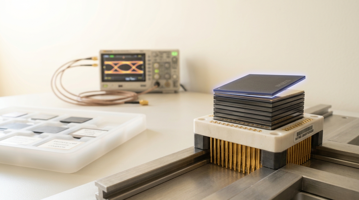
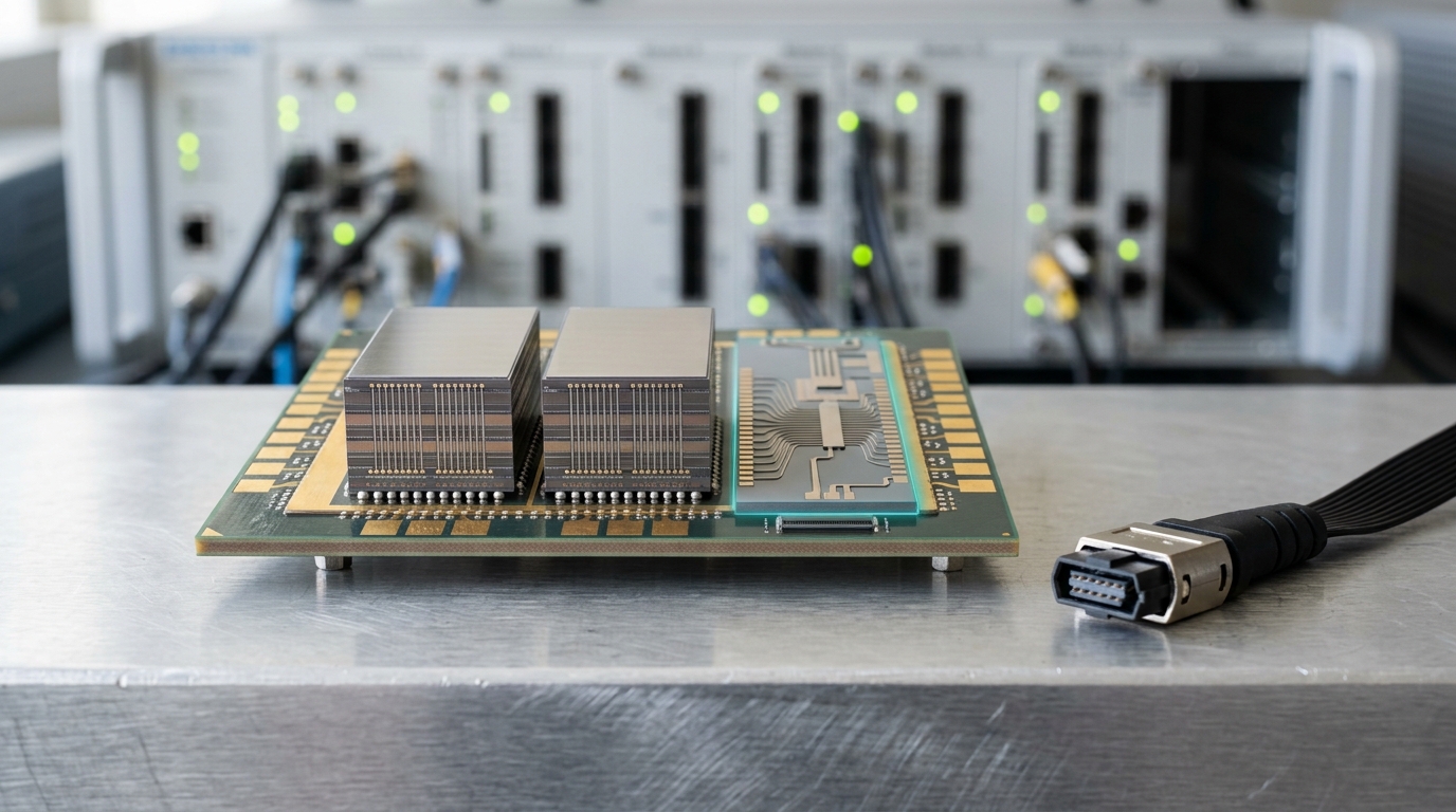
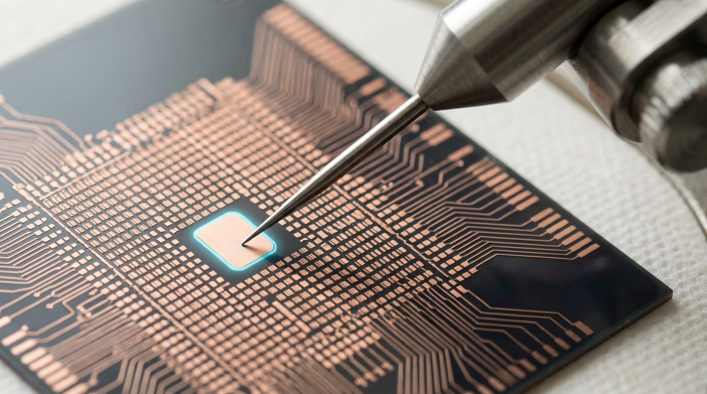
Physically, an HBM device is a short stack of DRAM dies bonded on top of a base logic die, connected vertically by through-silicon vias (TSVs): copper-filled channels that run the full thickness of each die, joined from one die to the next by fine microbumps, so that a signal can travel straight up through the stack rather than out to the edge of each die and back onto a package trace. The base logic die fans those vertical connections out, through a redistribution layer, to a silicon interposer — a purpose-built substrate, distinct from an ordinary circuit board, whose trace pitch is fine enough to carry the stack’s very wide, comparatively low-swing interface the short distance to the neighbouring compute die without the signal loss that distance would otherwise cost at these data rates. The interposer is what lets the memory sit beside the processor rather than across a board from it, and that short, wide, low-swing path is the actual mechanism by which HBM buys bandwidth: not a faster wire, but many more of them, run a much shorter distance.
JEDEC’s HBM3 standard, published as JESD238 in January 2022, quantifies exactly how that width is organized. It doubles the per-pin data rate of its predecessor to 6.4 gigabits per second, yielding up to 819 gigabytes per second per device; it doubles the number of independent channels to sixteen, with two pseudo-channels per channel giving thirty-two addressable sub-channels in total; and it defines per-layer densities from 8 to 32 gigabits, stacked 4-high, 8-high or 12-high, with headroom reserved for a future 16-high configuration [1]. None of those numbers describes a faster transistor. They describe a wider one: more independent channels, each individually modest, running in parallel across a stack whose dies are wired together vertically rather than laid out flat. The Gholami and colleagues survey of the resulting trend line is the clearest published statement of why this matters at all: across roughly two decades of hardware, peak server hardware compute has scaled at about 3.0 times every two years, while DRAM bandwidth has scaled at only about 1.6 times and interconnect bandwidth at about 1.4 times over the same interval [12]. HBM’s TSV-and-interposer construction is the industry’s most direct response to that widening gap — not a way around the DRAM cell’s physics, but a way to buy as much parallel width from it as packaging currently allows.
The quantity that decides who waits
Given a memory system built this way, the question for any specific piece of computation is simple to state and consequential to answer: for this kernel, is the bottleneck the arithmetic units or the memory system that feeds them? The quantity that answers it is arithmetic intensity, defined as the number of floating-point operations a kernel performs per byte it moves across the memory boundary that matters. Williams, Waterman and Patterson formalized the relationship between intensity and attainable performance as the roofline model:
with
Autoregressive decoding in a large language model is the sharpest illustration available today. Generating one token requires reading the entire set of model weights, plus the accumulated key-value cache, once each — a huge volume of bytes — to perform comparatively few floating-point operations per byte read, which places single-token decoding firmly on the memory-bound side of the ridge regardless of how fast the arithmetic units are [10]. A concrete device number makes the consequence tangible. AMD’s MI300X accelerator carries a theoretical HBM3 bandwidth ceiling of 5.3 terabytes per second; independent testing at Chips and Cheese ties that ceiling directly to a token-generation rate by noting that streaming a roughly 70-billion-parameter model’s weights through that bandwidth limit once per generated token caps throughput at only about 37 tokens per second in their own worked calculation, regardless of how much idle arithmetic capacity the accelerator still has on hand [15]. That is arithmetic intensity made visible as a wall-clock number: the compute units are waiting, not working, and the roofline model is the reason that outcome was predictable in advance rather than discovered after the fact.
Memory outside the package: how CXL.mem actually works
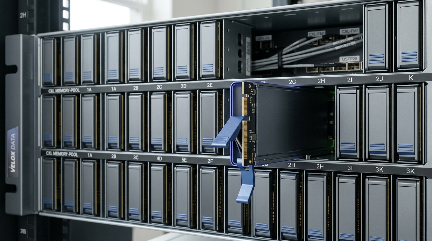
HBM solves the bandwidth side of the memory problem by sitting as close to the die as packaging allows. It does nothing for the capacity side — an HBM stack is small, expensive, and fixed at manufacturing time — and a workload whose working set simply will not fit needs a different mechanism entirely. That mechanism is the Compute Express Link, an interconnect built on top of the PCI Express physical layer that lets a host treat memory attached to a separate device as though it were local, while remaining a genuinely distinct piece of hardware that can be added, removed, or shared.
CXL is not one protocol but three, dynamically multiplexed over a shared electrical link: CXL.io, which handles device discovery and configuration much as PCIe itself does; CXL.cache, which lets an attached device participate coherently in the host’s cache hierarchy; and CXL.mem, which is the one that matters for memory expansion, giving a host direct load and store access to a device’s memory at 64-byte cache-line granularity — the same granularity a processor already uses to move data between its own cache and DRAM [3]. That granularity is the protocol’s central design choice: it is what lets software address CXL-attached memory as ordinary memory pages rather than as a block device that must be explicitly read and written, which is what makes memory pooling and expansion transparent to an unmodified application in the first place.
CXL 2.0 added switch-based pooling, so that a host could draw one or more memory devices from a shared pool rather than owning fixed, stranded capacity outright; CXL 3.0 extended that further with multi-level switching supporting up to 4,096 end devices, doubled per-pin bandwidth relative to CXL 2.0 while holding latency flat, and added coherent memory sharing, so a single region of CXL-attached memory can be visible to more than one host at once [2]. Two production-oriented systems research results show what that protocol capability is actually worth. Li and colleagues built Pond after finding, across a hundred production cloud clusters, substantial amounts of memory sitting stranded and effectively untouched on individual servers because it could not be reassigned elsewhere; Pond uses CXL’s load-and-store pooling access to treat that memory as a shared, allocatable resource instead, meeting cloud latency targets while measurably cutting DRAM cost [4]. Meta’s TPP takes the complementary position inside a single host with a mix of local and CXL-attached tiers: it is a transparent, OS-level mechanism that identifies hot and cold memory pages from real access patterns and migrates cold pages out to the slower CXL tier while promptly promoting hot pages back, evaluated on production servers with early CXL 1.1-capable hardware and found to come within about one percent of an ideal all-local-memory baseline, roughly eighteen percent better than a default Linux configuration [5].
What neither of those systems papers can settle on its own is whether CXL memory behaves, on real silicon, the way its specification promises — and that is precisely the gap Sun and colleagues closed by testing genuine CXL-ready hardware rather than a simulator: a fourth-generation Intel Xeon platform paired with three commercially available CXL memory devices from different manufacturers. Their central finding is that a real CXL memory device’s behavior is not adequately captured by the simplified latency-and-bandwidth models earlier work had assumed, and that a policy designed around the actual measured characteristics of genuine devices improved the performance of memory-bandwidth-intensive applications by up to twenty-four percent over one that assumed idealized CXL behavior [6]. That result is a direct instance of why this article’s source strategy insists on device measurements rather than specification numbers alone: a protocol’s paper capability and a shipping device’s measured behavior are related but distinct facts, and only the second tells a system builder what to actually expect.
The cache that grows while you watch
Nowhere does the interaction between capacity, bandwidth, and arithmetic intensity show up more concretely than in the key-value cache a transformer accumulates during autoregressive generation. At each layer, self-attention needs the key and value vectors for every token generated so far, and rather than recompute them at every subsequent step, an inference server stores them — the KV cache — and appends to it one token at a time.
Hooper and colleagues, working on KV cache compression for very long contexts, state the resulting footprint precisely: for a model with
which grows linearly in both batch size and sequence length, with the leading factor of two accounting for storing both keys and values [9]. That single equation is the whole mechanism: nothing about it is a design choice an inference engineer can simply decline. Extend the conversation, and
That growth hits both of the constraints this article has been building toward at once. It is a capacity problem, because a cache that no longer fits in HBM has to spill to CXL-attached or host memory, paying that link’s added latency and bandwidth tax on every subsequent read. And it is simultaneously a bandwidth problem, because — as established above — generating each new token requires streaming the entire accumulated cache through the arithmetic units again, so a larger cache means more bytes to move per token even when nothing about the arithmetic per token has changed at all. Pope and colleagues’ architectural response, multiquery attention, targets exactly this: sharing key and value projections across many query heads shrinks the per-token bytes that must be written to and streamed back out of the cache, which the authors report allows context lengths up to roughly thirty-two times longer at a given memory budget, precisely because the bandwidth actually spent moving the cache — not the arithmetic — was the binding constraint being relieved [10]. Nothing about attention’s mathematics changed; the bytes the mechanism has to move did.
Moving the compute instead of the data
Every mechanism described so far accepts a fixed premise: that arithmetic happens in one place, memory lives in another, and the job is to move bytes between them as cheaply as possible. Near-memory and in-memory computing reject that premise directly, by putting a small amount of arithmetic capability inside or immediately beside the memory array itself, so that at least some operations never generate a byte that has to cross the boundary at all.
Samsung’s Function-In-Memory DRAM, presented at the 2021 International Solid-State Circuits Conference and later commercialized as HBM-PIM, is the clearest production-adjacent example. Built on a 20-nanometer process as a 6-gigabyte device based on the HBM2 standard, it integrates a programmable computing unit rated at 1.2 teraflops directly into the stack, driven by exploiting bank-level parallelism — running many banks’ worth of simple arithmetic in parallel inside the memory itself rather than shipping each bank’s contents out to a separate processor first [7]. Samsung’s own account of the technology, and of AMD’s subsequent evaluation of it, frames the benefit explicitly as a vendor claim rather than an independently audited result: Samsung states the architecture has the potential to double the performance of a GPU accelerator while reducing its energy consumption, and reports that AMD, presenting further results at ISSCC in 2023, found up to an eighty-five percent reduction in the energy specifically spent moving data during in-memory processing compared with moving that same data out to a separate compute die [8]. Those are the vendors’ own reported figures, not a third-party benchmark, and should be read with that provenance attached.
The general principle behind that specific device is older and better characterized in the academic literature. Mutlu and colleagues’ survey of processing-in-memory approaches frames the whole family of techniques — from adding simple fixed-function logic near a memory bank, to exploiting a memory array’s own analog physics to perform bulk bitwise operations in place — around one unifying goal: reducing or eliminating data movement between memory and compute, rather than trying to make that movement faster [13]. Framed against the arithmetic-intensity argument above, near-memory computing is not a rival to CXL and HBM so much as a third, structurally different lever on the same problem. HBM buys bandwidth by making the path to memory wide. CXL buys capacity by making memory shareable across a network of hosts and devices at some added latency cost. Near-memory computing buys neither, directly — instead, for the narrow set of operations it can perform locally, it removes the trip altogether, which is the one move that a wider path or a better-managed pool can never fully replace, because no amount of bandwidth makes a trip that was never necessary go any faster than not taking it.
Where the mechanism is likely to move
These are forecasts, kept explicitly separate from the sourced mechanisms above. Horizon: 15 August 2029. The assumptions are that the compute-versus-bandwidth divergence documented by Gholami and colleagues continues at a broadly similar rate, that DRAM’s cell-level physics do not change fundamentally within this window, and that transformer-family inference remains the dominant AI serving workload.
One. Mainstream accelerators will ship with a higher roofline ridge point in 2029 than in 2026 — that is, a larger share of production inference and training kernels will be memory-bound at a given arithmetic intensity than is true today. Indicator: published microbenchmark studies of successive accelerator generations. Disconfirmed if a mainstream training or inference accelerator ships whose measured ridge point is lower than its direct predecessor’s.
Two. CXL-attached memory tiers will be deployed increasingly for KV cache offload specifically, rather than only for general-purpose capacity expansion, because the KV cache’s linear growth in sequence length and batch size makes it the single most predictable and fastest-growing consumer of capacity in an inference fleet. Disconfirmed if production inference stacks in 2029 still treat KV cache overflow chiefly by truncating or evicting context rather than by tiering it onto a slower memory class.
Three. Near-memory and in-memory compute will remain confined to a narrow set of operations — reductions, simple elementwise arithmetic, bulk bitwise work — rather than displacing general-purpose accelerators, because the economics of specialized silicon inside a commodity memory die favor operations simple and common enough to amortize the design cost. Disconfirmed if a near-memory or in-memory design ships within this window capable of executing general dense matrix multiplication competitively with a dedicated accelerator at comparable cost.
What to take away
A byte’s trip from a DRAM cell to an arithmetic unit is not one mechanism but four, stacked on top of each other, each with its own physics and its own failure mode. The cell trades speed for density once, permanently, in silicon. The stack recovers bandwidth from a slow cell by running thousands of narrow vertical paths in parallel through TSVs and a fine-pitch interposer, buying width rather than speed. The protocol lets memory live outside the package by paying a real, measured latency tax at 64-byte granularity, and that tax is only knowable by testing genuine hardware, not by reading a specification. And a growing cache turns an architectural choice — how attention is computed — into an arithmetic inevitability, where every additional token written is a fixed number of additional bytes that must be moved on every step from then on.
None of these four mechanisms is optional, and none of them is fixable by the others. More SRAM does not repair a leaking DRAM cell. A wider HBM stack does not give a workload capacity it does not have. A larger CXL pool does not remove the latency of reaching it. And moving compute next to memory only helps for the narrow set of operations simple enough to move there. The bandwidth wall is not one wall. It is the sum of four separately negotiated ceilings, and understanding an AI system’s performance means knowing, for any given operation, which of the four is actually the one being run into.