Two problems wearing one name
Talk to enough hardware architects about “the memory problem” in AI systems and it becomes clear the phrase hides two distinct problems that arrived in different decades, from different pressures, and that current AI infrastructure now has to solve simultaneously. One is a speed problem: the rate at which data can move between a processor and its memory has grown far more slowly than the processor’s own arithmetic throughput, a gap given a name by two researchers in the mid-1990s [4]. The other is a capacity problem: how much data a system can hold close enough to compute on, at a price a datacenter operator will actually pay for enough of it. High-Bandwidth Memory answers mostly the first problem. Compute Express Link exists mostly because of the second. Neither technology was designed with large language models in mind — HBM predates the modern transformer by four years, and CXL’s founding predates it by months — and both were shaped instead by decades of ordinary commodity-memory economics.
This is a dated, sourced account of that lineage: the cell, the chip, the standard, the product, the update. It is not a technical explainer of how any of these technologies work internally; the pilot article in this series already does that work for the memory hierarchy generally. It is a history, told through the documents and announcements that fix each step to a specific year, with vendor claims marked as claims and with the places where the record is genuinely contested left contested rather than resolved.
The one-transistor cell and the first commercial chip
In 1966, at IBM’s Thomas J. Watson Research Center, Robert Dennard proposed storing one bit of memory as charge on a capacitor accessed through a single transistor — a design far simpler than the six-transistor static cells and magnetic-core memory it competed against, and one that could be shrunk far more aggressively. IBM filed for a patent on the idea and was granted US Patent 3,387,286 in 1968 [1]. It took four more years for a commercial version of that cell to reach the open market: Intel’s 1103, introduced in October 1970, packed 1,024 of Dennard’s one-transistor cells into an 18-pin package. Within about a year it was, by Intel’s own account, the best-selling semiconductor device in the world, and by 1972 fourteen of the eighteen mainframe manufacturers across the United States, Europe and Japan had adopted it, displacing magnetic-core memory as the industry default [3]. Dynamic random-access memory — DRAM — has held that default position for main memory ever since. Every technology discussed in the rest of this article either is DRAM, packages DRAM more densely, or exists specifically to route around one of DRAM’s limits.
Dennard did not stop at the memory cell. In 1974, with five IBM colleagues, he published the scaling theory that let a transistor shrink in every dimension while holding its electric field constant — smaller, faster, and, crucially, no hotter per unit of area [2]. That relationship, later called Dennard scaling, is a large part of why processor clock speeds climbed for three decades without a matching climb in power density. It also set up the imbalance that would eventually get a name: the same scaling discipline that let logic transistors shrink and speed up did not apply with equal force to a DRAM array’s row and column access times, which are governed by different physics entirely — charge leaking off a capacitor, and the resistance and capacitance of a long shared wordline, neither of which shrinks the way a logic gate’s switching delay does. Static RAM, built from six-transistor cells rather than one, stayed faster than DRAM for exactly this reason, at several times the area and cost per bit — which is why cache hierarchies have always kept a little SRAM close to the arithmetic units and a great deal of DRAM further away, rather than the reverse.

A gap gets a name
By the early 1990s the divergence Dennard’s own scaling theory implied was measurable rather than theoretical, and in 1994 two researchers at the University of Virginia wrote it down. Professor William Wulf and his then-graduate student Sally McKee argued that if processor speed kept improving faster than DRAM speed, an increasing share of every program’s running time would be spent waiting for memory rather than computing, regardless of how fast the arithmetic units themselves had become. Their short, deliberately provocative note was published the following year in ACM’s Computer Architecture News. UVA’s own retrospective on the paper, published in 2022, credits Wulf and McKee with identifying “what would become a defining challenge in computer science for decades to come” [4] — and it is worth flagging plainly that this is a university crediting its own faculty with a landmark result, a fact a careful reader should weigh even though the underlying observation about processor-memory divergence has since been independently reconfirmed by direct hardware measurement many times over, in different eras, on different hardware, by different groups with no institutional stake in the claim.
The name mattered because the mechanism it described did not go away. It moved, generation after generation, into whatever was that era’s newest fast memory tier — first DRAM against SRAM cache, then GDDR against a GPU’s shader array, then HBM against a tensor core, and eventually CXL-pooled memory against everything on the same board. Each of the sections below is, in effect, a different decade’s specific answer to Wulf and McKee’s general observation.
Standardizing the everyday store
Memory chips became genuinely interchangeable commodities only once an industry body wrote down, in public, exactly how a chip from one factory had to behave in order to work in a socket built by another. JEDEC, the semiconductor engineering-standards body, published its Double Data Rate SDRAM specification, JESD79, in June 2000 [5], codifying DDR SDRAM’s ability to transfer data on both edges of the clock rather than one. DDR and its JEDEC-numbered successors — DDR2, DDR3, DDR4 and DDR5 — became, and remain, the default main memory of general-purpose computing: optimized first for density and cost per bit, and only secondarily for peak bandwidth, because a server or a desktop system’s economics have always rewarded holding more over moving faster.
Graphics workloads wanted the opposite trade, and JEDEC eventually standardized a separate lineage for it. Graphics DDR memory diverged specifically to serve a GPU’s much wider, much hungrier memory bus; JEDEC published JESD212, the GDDR5 SGRAM standard, in December 2009 [6]. GDDR5 and its successors trade the tight per-bit cost that server DRAM needs for a much wider bus run at higher per-pin data rates — a specialization built for framebuffers and shader arrays years before anyone ran a general-purpose numerical kernel on the same silicon. When general-purpose GPU computing arrived in earnest in the following years, it inherited GDDR memory as a side effect of running on graphics hardware, not because GDDR had been chosen as a compute memory technology on its own merits. Independent microbenchmarking of exactly this era’s GPUs — Fermi, Kepler and Maxwell among them, all GDDR5-class parts pressed into scientific and early machine-learning workloads — found it necessary to measure global-memory throughput and latency directly on real hardware, rather than trust the advertised peak figures, because the two routinely diverged in practice [7]. That divergence is a smaller, concrete rehearsal of the same argument Wulf and McKee had made in the abstract fifteen years earlier, now visible on a specific, purchasable graphics card doing someone else’s arithmetic.
The scale of that abstract argument, made concrete decades later, is stark. Gholami and colleagues, surveying twenty years of server hardware, report that peak hardware FLOPS scaled at roughly 3.0 times every two years while DRAM bandwidth scaled at only 1.6 times and interconnect bandwidth at 1.4 times over the same interval [13]. Those are compounding rates, and compounding rates diverge violently over long periods. If the two multipliers applied uniformly across a full twenty years — an extrapolation the source itself does not perform, offered here only to size the shape of the problem, not as a number the cited paper states — the ratio between available arithmetic and available bandwidth grows as
with
JEDEC standardizes a die stack
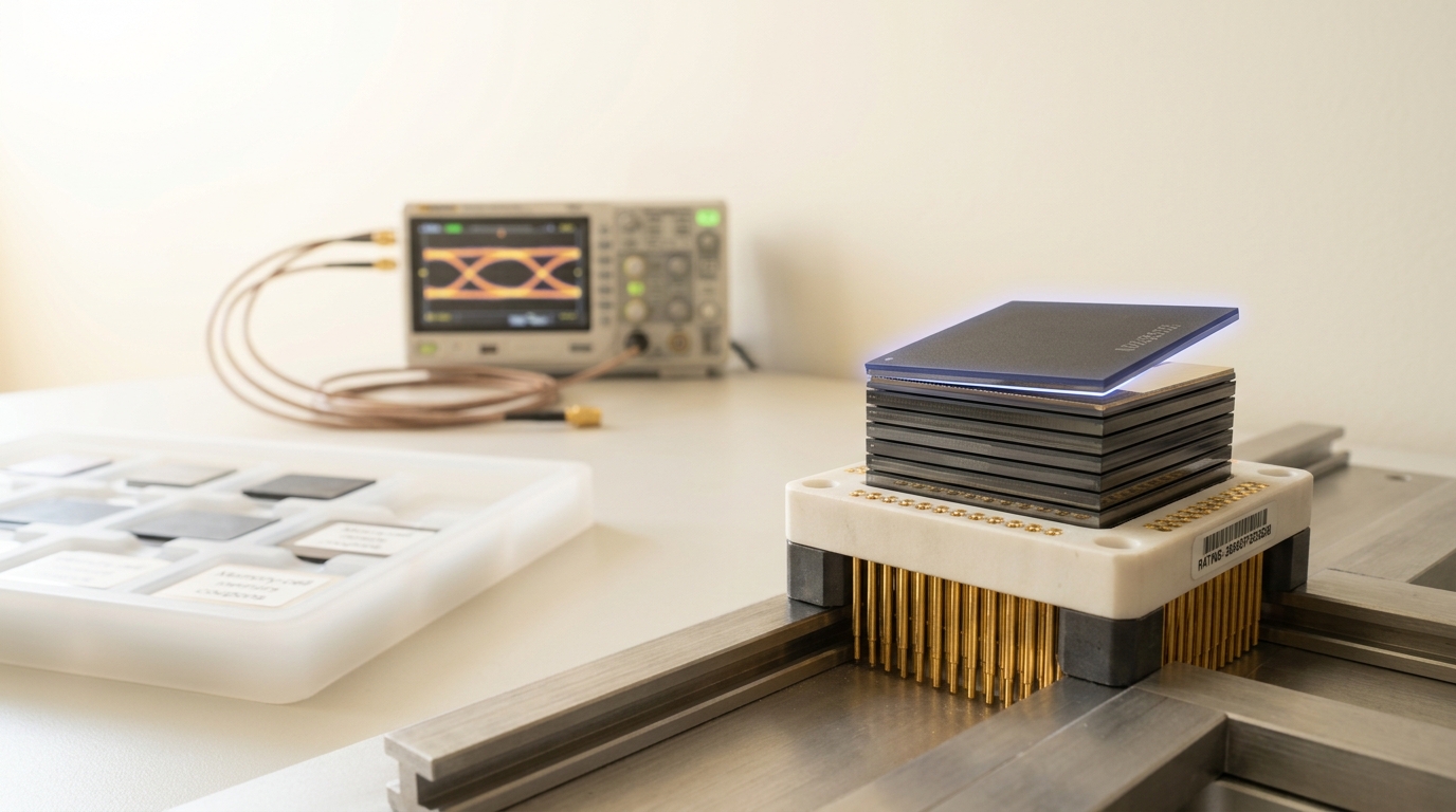
The specific answer for compute silicon that could no longer tolerate GDDR’s distance across a printed-circuit board was to stop routing memory to the processor over a board trace at all, and instead stack multiple DRAM dies vertically, connect them through silicon vias drilled straight through each die, and mount the resulting stack next to the compute die on a shared silicon interposer. JEDEC formalized the result as JESD235, “High Bandwidth Memory (HBM) DRAM,” in October 2013 [8] — a specification developed with substantial technical input from AMD and SK hynix, who had jointly built a working through-silicon-via HBM part the following year, in 2014, by SK hynix’s own account of its product history [10].
The first commercial product built on that standard reached the market in the middle of 2015. AMD’s Radeon R9 Fury X, built around the Fiji GPU, was announced on 16 June 2015 and went on sale on 24 June, in an AMD press release that called it the world’s first graphics family with HBM technology, claiming sixty percent more memory bandwidth than the GDDR5 card it replaced across a 4096-bit memory interface, and more than three times the performance per watt of GDDR5 in ninety-four percent less printed-circuit-board area [9]. That last board-area figure is a vendor’s own comparative claim and should be read as one; the underlying architectural fact behind it — a much wider memory bus fit into a much smaller footprint by moving the DRAM off the board edge and onto the package itself — is not in dispute, since it is the entire mechanical premise of stacked memory rather than a performance claim requiring independent replication.
Iterating the stack
The first HBM standard was conservative by later measures: on the order of 128 gigabytes per second and 4 gigabytes of capacity per stack in its original 2013 form. JEDEC kept revising it. By the time of the JESD235B update, publicly reported in December 2018, the same standardized family had been extended to densities up to 24 gigabytes per device at speeds up to 307 gigabytes per second, across stack configurations from two-high up through twelve-high [11]. In between those two points, JEDEC’s HBM2 generation reached compute GPUs directly: NVIDIA announced its Pascal-based Tesla P100 accelerator on 5 April 2016, at that year’s GPU Technology Conference, specifying 16 gigabytes of HBM2 memory delivering 720 gigabytes per second — more than three times the bandwidth of the Maxwell generation it replaced [12]. SK hynix’s own account of its product line separately places its HBM2E mass production, which the company describes as the industry’s first, in 2020, and describes announcing HBM3’s development in October 2021, beginning HBM3 mass production in June 2022, and supplying HBM3 to NVIDIA systems from the third quarter of that year [10]. Those last claims are a single vendor’s characterization of its own priority in a competitive field with several capable suppliers, and should be read as a vendor’s claim rather than an independently adjudicated “first” — this article does not attempt to referee competing priority claims across memory manufacturers.
None of those revisions solved the other problem. HBM buys bandwidth specifically by sitting physically next to the compute die, and that same proximity caps how much of it can ever fit: a fixed number of stacks, on a fixed-size interposer, bounded by a lithography tool’s reticle limit. A processor with more HBM than its predecessor almost always still has far less total addressable memory than an equivalent system built around ordinary, off-package DRAM, because ordinary DRAM was never subject to the same packaging constraint in the first place. Capacity and bandwidth, in other words, kept being two different limits with two different remedies — exactly the distinction the industry would eventually need a different kind of interconnect to address directly.
An interconnect built for the other problem
Compute Express Link was announced in March 2019 as a new cache-coherent interconnect, built on the physical layer of PCI Express, aimed squarely at the workload class that HBM’s packaging constraint could never serve: attaching memory, and memory-holding accelerators, to a processor at capacities and in pooling arrangements a fixed on-package stack could never reach [14]. The consortium that formed around the specification — with Alibaba, Cisco, Dell EMC, Facebook, Google, Hewlett Packard Enterprise, Huawei, Intel and Microsoft among its founding members — incorporated formally that September, and released the CXL 1.1 update roughly six months after the original 1.0 specification, adding errata fixes and a compliance chapter [14].
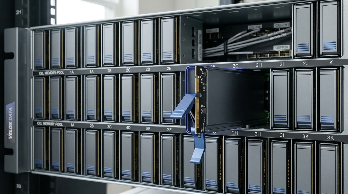
The features that made CXL specifically a capacity technology, rather than merely another interconnect, arrived in its second and third major revisions. CXL 2.0, released in November 2020, added switching and memory pooling: the ability to fan a single host out to multiple downstream devices, and to let several hosts draw on a shared pool of memory dynamically instead of each owning a fixed allocation that sits idle whenever that particular host does not need it [15]. CXL 3.0, released on 2 August 2022, extended the same idea into genuine fabric-level topologies — multiple switches, peer-to-peer device communication, and fine-grained resource sharing across more than one host domain at once — while doubling the link’s per-lane data rate over CXL 2.0 without adding latency [15]. Both revisions target precisely the DRAM-utilization problem that on-package HBM cannot touch: idle, stranded capacity sitting behind one host that a neighboring host, starved for memory, has no way to reach.
Academic and industry research has since measured what pooled CXL memory actually costs and buys in production. Li and colleagues, describing a memory-pooling system called Pond built from Meta’s own cloud-fleet traces, report that pooling across as few as eight to sixteen sockets captures most of the achievable benefit, that CXL-attached memory behaves latency-wise like roughly one NUMA hop on a modern two-socket server, and that their design reduced DRAM costs by about seven percent while keeping application performance within one to five percent of memory allocated on the same node as the compute using it [16]. That NUMA-hop latency figure sits at the center of a genuine, unresolved disagreement among systems architects. Some treat CXL-pooled memory as a plausible tier for latency-tolerant capacity — plausibly including the very large, heavily reused key-value caches that long-context language-model serving now generates, since a cache entry read many times can absorb one extra hop far more easily than a value read once. Others argue that any added hop at all disqualifies CXL from the tightest inner loops of AI serving, and see its near-term value chiefly in ordinary cloud virtual-machine memory provisioning rather than in accelerator-adjacent AI workloads specifically. Both positions are consistent with the same measured latency number; they differ on how much latency a given workload’s access pattern can absorb, which is an empirical property of each deployment rather than a fixed property of CXL itself, and the disagreement is not yet settled by the published evidence either way.
Where the two threads meet
Two separate historical threads converge inside a contemporary AI accelerator. The bandwidth thread runs from Dennard’s one-transistor cell through the naming of the memory wall, through GDDR’s unplanned conscription into GPU compute, to HBM’s answer of sitting DRAM directly on the compute package — a lineage aimed entirely at feeding a fast arithmetic unit fast enough that a kernel is not, in the vocabulary this literature settled on, memory-bound. The capacity thread runs separately, out of the same commodity DDR economics, through the recognition — formalized in CXL — that a fixed on-package stack could never hold everything a modern workload wants resident at once, however fast that stack could be read.
Both threads land in the same accelerator today for a specific, workload-level reason: arithmetic intensity, the ratio of computation performed to bytes moved, is not a fixed property of a chip. It is a property of a workload run against a chip, and large language model inference in particular generates a historically unusual pressure on both axes simultaneously, through its key-value cache. That cache must be kept resident across a whole generation session — a capacity demand — and it must also be streamed through the arithmetic units on every single token produced — a bandwidth demand, applied to the same bytes, over and over, for as long as the conversation continues. Near-memory and processing-in-memory research designs, which move a small amount of computation into or beside the memory array itself rather than always moving data out to a separate arithmetic unit, are the research community’s most direct response to a blunt observation: neither HBM’s bandwidth nor CXL’s capacity, purchased separately, changes how many bytes still have to cross a wire in the first place. That direction remains a live, unsettled research program rather than a shipped standard, and is a separate history from the one told here.
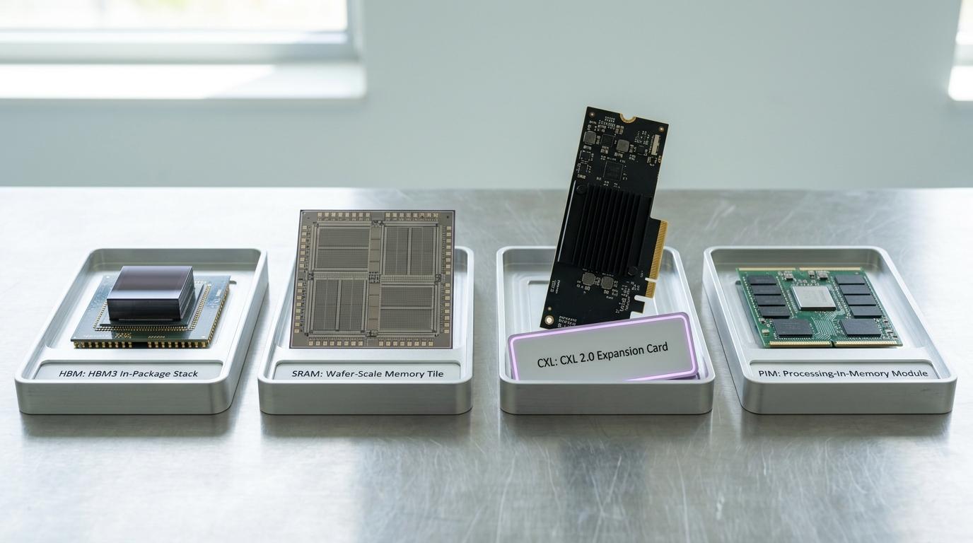
None of this was planned as a coherent system by any single actor. Dennard did not design a one-transistor capacitor cell anticipating a future bandwidth wall; JEDEC did not standardize GDDR anticipating general-purpose GPU compute; the CXL consortium’s founding members did not incorporate anticipating transformer key-value caches, which did not yet exist under that name. Each step solved the specific, dated problem in front of it, using the specification and the product that a specific, named set of companies actually designed, standardized and shipped in a specific year. What is left, roughly sixty years after Dennard first proposed the cell, is a stack of memory tiers — on-die SRAM, HBM, CXL-pooled DRAM, and ordinary commodity DDR beyond that — each one a documented, dated answer to a distinct, narrowly specific shortfall, now sitting together in service of a workload that none of their original authors had any way to anticipate.