One label, two different achievements
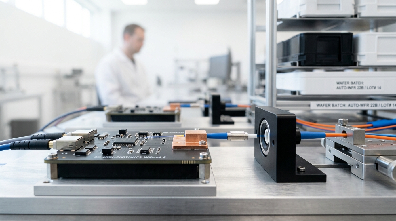
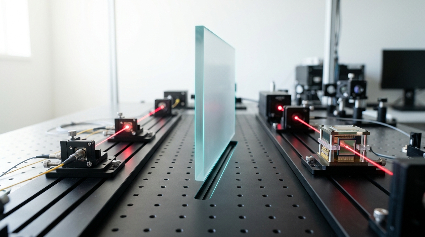
A crucial distinction has emerged in 2026 coverage of “photonic computing” that this briefing wants to make explicit before going further: photonic interconnect uses light only to move data between chips, while photonic compute uses light to perform the actual arithmetic itself [2]. Only the second category is “computing with light” in the sense the phrase implies. The first category is a genuinely important, already-commercializing technology this cohort’s power-and-optics track covers directly — but it is not the more speculative, more novel claim this briefing is actually assessing.
What the interconnect side already does
Optical interconnect replacing copper for chip-to-chip and rack-to-rack data movement is real, funded, and shipping — this cohort’s companion briefing on optical interconnect covers the commercial deployment case in depth. It solves a specific, well-understood bottleneck: as AI accelerator clusters scale, moving data between thousands of chips fast enough, without prohibitive power loss, becomes a binding constraint copper interconnect increasingly cannot meet. This is the less novel, more mature half of “photonic computing,” and treating its progress as evidence that optical arithmetic is equally mature would overstate the more speculative claim.
What the compute side is actually attempting
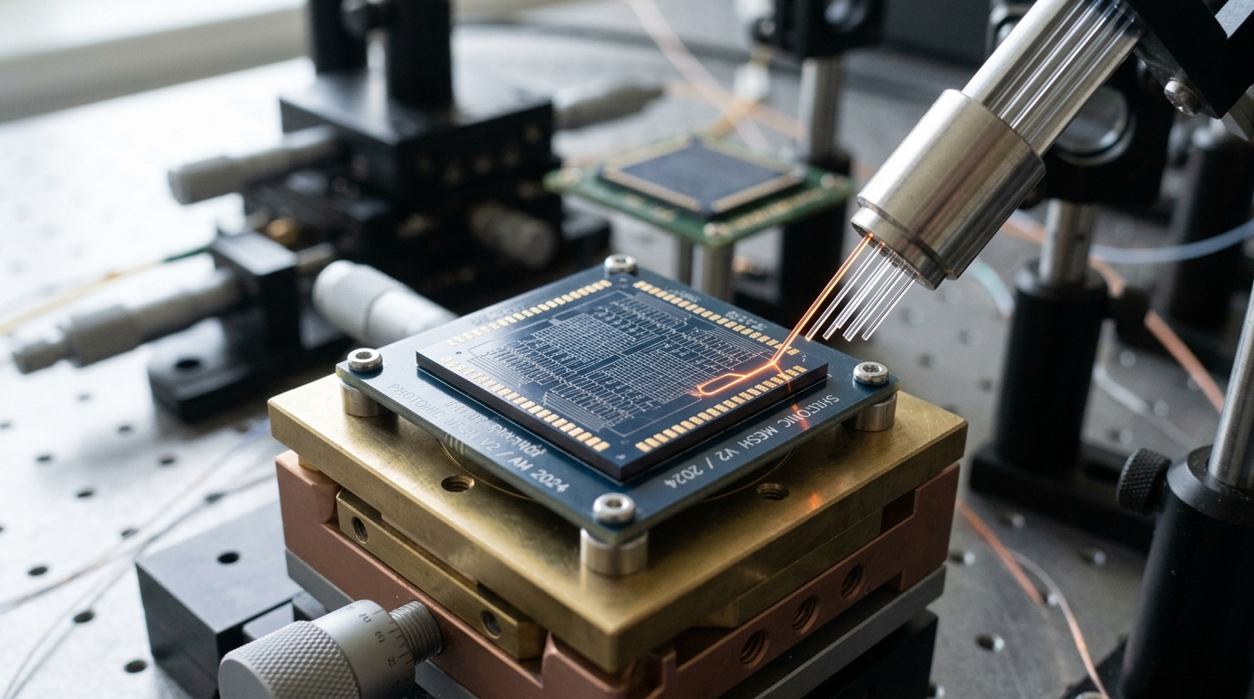
Lightmatter, whose compute chip is called Envise, and Lightelligence, whose chip is called PACE (Photonic Arithmetic Computing Engine), both build hardware that performs actual AI math using light rather than electronic transistors [1]. Lightmatter pursues a dual-engine strategy: Passage, its interconnect product, and Envise, its compute product, developed in parallel rather than as a single blurred offering — itself evidence the company treats the interconnect/compute distinction as real and commercially significant, not just an academic one. Lightelligence’s PACE targets optimization problems specifically — the kind relevant to finance, manufacturing, and logistics — rather than general neural-network training [2].
The genuinely encouraging research signal
Independent research in 2026 reports photonic computer chips performing comparably to purely electronic counterparts on raw performance benchmarks for specific workloads — a meaningful technical validation that optical compute is not purely theoretical [3]. Separate coverage frames this as chips that “do math with light” achieving genuine parity with electronic chips on the tasks tested [4]. That is a real result. It is also, by the nature of early-stage technology validation, a result on specific benchmark tasks rather than proof of general-purpose readiness to replace electronic AI accelerators at the scale this cohort’s Nvidia and custom-silicon coverage documents.
Why “niche” is not the same as “dead end”
The honest 2026 assessment sits between the two extremes a headline might reach for: photonic compute is neither a mature, ready-to-scale alternative to electronic AI silicon, nor a dead-end research curiosity. It is a genuinely promising, still-narrow technology with real performance validation on specific workloads, built by companies — Lightmatter and Lightelligence chief among them — with real funding and real shipping interconnect products generating revenue in the meantime. Whether the compute side scales from validated benchmark parity to broad commercial deployment is not yet answered by the sources available as of 2026, and this briefing does not claim to answer it in advance of that evidence existing.
Where this fits against this cohort’s other novel-technology coverage
Read alongside this cohort’s companion briefings on quantum computing and neuromorphic chips, photonic compute occupies a similar position: a real, technically validated, well-funded approach to computing that remains meaningfully earlier-stage than the electronic AI accelerators covered throughout the rest of this cohort. None of these three adjacent fields currently threatens to displace classical AI silicon in the near term — each is worth tracking as a genuinely separate technology story, not as a competing horse race against the industry this cohort spends most of its pages covering.
What would have to be true for optical compute to scale past benchmarks
Moving from validated benchmark parity to broad deployment would require optical compute chips to clear several practical hurdles this briefing’s sources do not yet report as solved: manufacturing yield at commodity semiconductor-fab scale rather than research-lab scale, integration with existing software stacks built around electronic accelerator assumptions, and a cost structure competitive with the electronic AI silicon this cohort’s other tracks document improving on its own trajectory every year. None of these hurdles is unique to photonic compute — this cohort’s neuromorphic-chip briefing documents a structurally similar set of adoption barriers facing brain-inspired hardware — but naming them explicitly is the difference between honest technology reporting and treating a promising benchmark result as though it were already a market-ready product.
The most useful way to track this story going forward
Rather than asking “will photonic computing replace GPUs,” a more answerable question for readers following this space is narrower: which specific workload categories, if any, does optical compute demonstrate a decisive efficiency advantage on first, and does a real commercial customer pay for that advantage at production scale. Interconnect already cleared that bar for data movement. Compute, as of 2026, has cleared the benchmark-parity bar but not yet the paying-customer-at-scale bar — a distinction worth tracking specifically, rather than treating “photonic computing” as one undifferentiated story that succeeds or fails as a single unit.