Four ways to avoid the same wall
Every mainstream AI accelerator, however fast, does arithmetic the same physical way: transistors switching on a shared clock, multiplying and adding numbers that are stored in memory sitting some physical distance from the arithmetic unit, moving those numbers back and forth across a bus for every layer of every model. That arrangement is over sixty years old, and improving it — smaller transistors, wider buses, more of both — has been most of the history of computing hardware. This article is about four devices that do the arithmetic a genuinely different way: a mesh of optical interferometers that multiplies by letting laser light interfere with itself, a chip that only computes when a neuron-like circuit crosses a voltage threshold, a grid of resistive memory cells that multiplies by Ohm’s law without ever separating the memory from the math, and a handful of qubits whose joint state is itself the object being operated on.
None of the four is a drop-in GPU replacement, and this piece does not rank them, compare their benchmarks, or judge how close any is to a shipped product — those are separate questions taken up elsewhere in this series. What follows is narrower: for each, what is the actual physical operation, which circuit performs it, and what does that operation cost in return for whatever it saves. Distinguish, throughout, three kinds of claim: a measured fact from a peer-reviewed paper, a figure a vendor reports about its own hardware, and this article’s own analysis of what that figure does and does not establish.
Multiplying matrices with interfering light
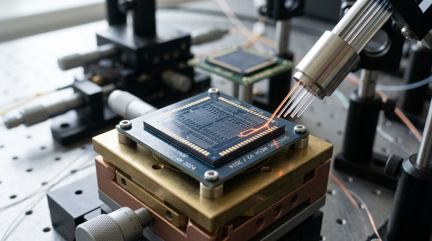
A large fraction of the arithmetic in a neural network is matrix-vector or matrix-matrix multiplication: every linear layer, and every projection inside an attention block, reduces to it. A photonic matrix multiplier performs that operation using the wave nature of light rather than a digital multiply-accumulate circuit, and the building block that makes this possible is the Mach-Zehnder interferometer (MZI).
An MZI is a two-mode optical device built from two 50:50 directional couplers and two phase shifters. One phase shifter, placed between the couplers, sets how the light interferes internally and therefore what fraction of the input power exits each of the two output ports; the second phase shifter sets the relative phase between the two outputs. Because these two adjustable phases are the device’s only free parameters, an MZI can be tuned to realize any rotation in the mathematical group SU(2) — any splitting ratio between its two output modes, at any relative phase [2].
A single MZI mixes two optical modes. To act on a vector of many modes at once, MZIs are wired into a mesh where every pair of modes crosses at some layer. Reck and colleagues showed in 1994 that a triangular arrangement of MZIs could implement an arbitrary N-by-N unitary matrix; Clements and colleagues later showed that rearranging the same MZIs into a rectangular lattice, so that every mode meets its nearest neighbor at the first possible opportunity, implements the same class of transformation in roughly half the physical depth. Both layouts use exactly N(N−1)/2 MZIs for an N-mode mesh, but the Reck triangle needs 2N−3 component layers end to end while the Clements rectangle needs only N — nine layers deep against fifteen, in a nine-mode example. Because optical loss and phase error accumulate with every component light passes through, the shallower layout also loses less light and tolerates fabrication error better [2].
An MZI mesh built this way implements a unitary matrix: a transformation that preserves the total optical power passing through it. Most matrices a neural-network layer actually needs are not unitary. The standard fix is a singular value decomposition, writing the desired matrix M as
where U and V* are unitary matrices, each realized by its own MZI mesh, and Σ is a diagonal matrix of non-negative singular values, realized by a bank of tunable optical attenuators placed between the two meshes. Light entering the chip passes through the first mesh, has each of its modes independently attenuated by the corresponding singular value, then passes through the second mesh — end to end, the optical power distribution leaving the chip is the matrix-vector product of M and the input vector encoded in the light entering it [1].
Shen and colleagues built and tested exactly this architecture: a programmable nanophotonic processor with 56 MZIs and 213 individually controlled phase shifters, forming a four-mode (SU(4)) interferometer mesh paired with a diagonal matrix multiplication core. They configured it as a four-layer, four-neuron-per-layer optical neural network — 48 phase-shifter settings in total — and used it for a spoken-vowel recognition task. The interferometer cores themselves ran with a measured fidelity of 99.8 percent; the fabricated chip classified 138 of 180 test vowels correctly (76.7 percent) against 165 of 180 (91.7 percent) in an ideal software simulation of the same network, a gap the authors attribute to accumulated fabrication and calibration error across the mesh rather than to any difference in the underlying algorithm [1]. This was a 2017 laboratory demonstration chip built to prove the architecture, not a shipped accelerator, and the accuracy gap it reports is itself a measurement of how far analog optical hardware still sits from its own noiseless design.
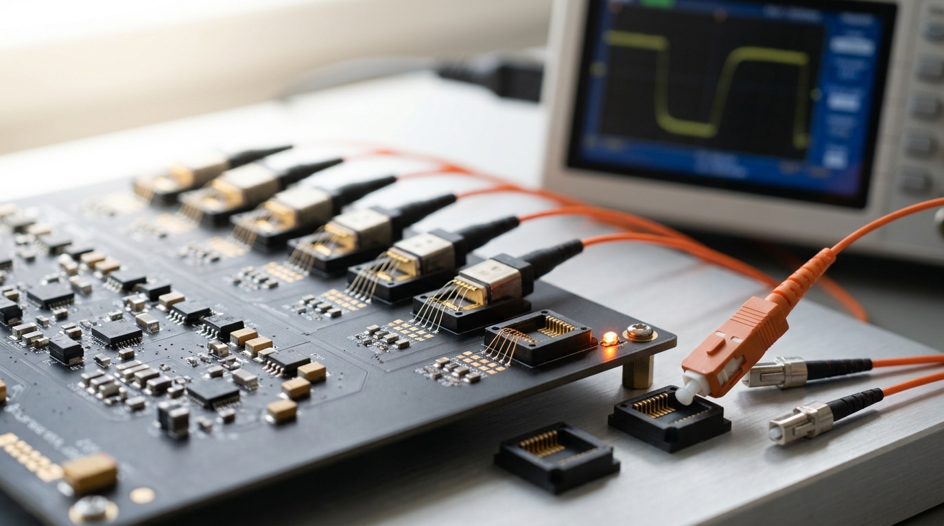
What actually happens physically, at each coupler, is interference: two incoming optical field amplitudes combine, and the coupler’s built-in geometry together with the local phase shifter determines how much of the combined field routes to each output waveguide through constructive and destructive interference between the two internal paths. Chain enough couplers together and a whole vector of input amplitudes cascades through the mesh, each output waveguide ending up carrying a weighted sum of every input — which is exactly a matrix-vector product, computed passively, at the speed and energy cost of light traveling a few millimeters across a chip, once the phase shifters have been set. No clock drives this process and no transistor toggles during it.
Getting an answer out means returning to electronics. A photodiode is a square-law detector: its photocurrent is proportional to optical power — the squared magnitude of the field, not its amplitude and phase directly — so a mesh’s design has to put whatever quantity matters into intensity before light reaches the detector, because phase not already converted into an intensity difference is simply lost at this step. The resulting photocurrent is tiny, nanoamps to low microamps, and has to be amplified by a transimpedance amplifier into a usable voltage before any further processing can happen. Shen and colleagues report photodetection at rates exceeding 100 gigahertz, but their own nonlinear activation function was applied electronically, after this optical-to-electrical conversion, rather than optically; they note that integrating a nonlinear optical element such as a graphene saturable absorber directly into the waveguide could eventually keep this step in the optical domain [1].
McMahon’s 2023 review of the physics underlying optical computing spells out why that conversion step, rather than the multiplication itself, is where the practical limits sit. Because of noise inherent to any physical analog computation — among other sources, the finite number of photons arriving per measurement and the thermal noise of the detector’s own readout amplifier — McMahon states plainly that it is difficult for any analog computer, optical or otherwise, to exceed roughly ten effective bits of precision. Neural-network inference tolerates that: simulations of deep optical networks running sixty optically executed layers matched the accuracy of the same network run digitally with 8-bit integer arithmetic; exact arithmetic is a different matter, and not what this class of hardware is for [3]. McMahon further argues that the computation inside the mesh can be close to free in energy terms, but every input vector must first be converted from electronics into an optical signal and every output converted back — that conversion overhead, not the interference itself, is where much of a photonic system’s real energy budget goes. His estimate is that a clear net energy advantage requires a vector dimension above roughly ten thousand, well beyond the four-mode and even few-hundred-mode meshes built to date [3]. He also names why nonlinearity is still handled electronically in nearly every demonstration: ordinary optical materials lack a strong single-photon nonlinearity, so a genuinely optical nonlinear operation currently requires either single-photon detection or engineered interactions across multiple modes, neither yet standard practice [3].
A neuron that only computes when it has something to report
A conventional accelerator evaluates every unit of every layer on every clock cycle, whether or not that unit’s output has changed. A neuromorphic chip is built around a different premise: a circuit that behaves like a single neuron, integrating its inputs and reporting a result only at the specific moment its state crosses a threshold.
At the circuit level, each neuron unit holds a membrane potential, implemented as a charge on a capacitor or a value in a small register, that accumulates incoming weighted spike inputs and simultaneously leaks — decays exponentially — toward a resting value between inputs. A standard discrete-time version of this leaky-integrate-and-fire rule is
where the s_i[t] are the incoming binary spike events, the w_i are the corresponding synaptic weights, and τ sets how quickly the leak dissipates unused charge. When V_m crosses a fixed threshold, the circuit emits a single digital pulse — a spike — on its output, and its membrane potential resets. Nothing is emitted, and in an efficient asynchronous implementation nothing is computed downstream, in any cycle where the threshold is not crossed.
Intel’s Loihi chip is a concrete, published example of this circuit style at scale. A single die, fabricated in Intel’s 14-nanometer process, integrates 128 fully asynchronous neuromorphic cores — there is no single clock driving every core in lockstep; each core processes and forwards spike events as they arrive — alongside three embedded x86 management cores. Across those 128 cores the chip holds 130,000 neurons and 130 million synapses, and Intel’s own reported figures put nominal operation at roughly 30 billion synaptic operations per second at about 15 picojoules per synaptic operation [4] — the paper’s own number for its own hardware and workload, not an independently reproduced comparison. Loihi’s synapses are also programmable in place: learning rules run as on-chip microcode generalizing pairwise spike-timing-dependent plasticity, so a weight update is computed locally, from the relative timing of the pre- and post-synaptic spikes at that synapse, rather than by a global backward pass over the whole network [4].
IBM’s TrueNorth, an earlier and architecturally distinct design, makes the same event-driven premise concrete in a different way. It arranges 4,096 neurosynaptic cores in a 64-by-64 grid on a single 5.4-billion-transistor chip; each core is built around a crossbar-style array of synapses coupled directly to its own bank of neuron circuits, so the memory holding that core’s synaptic weights sits physically inside the same core that computes with them, rather than across a shared bus. Across the whole chip that yields 1 million neurons and 256 million configurable synapses. Communication between cores runs over an asynchronous address-event routing network: a spike is represented as a short packet naming only the neuron that fired, delivered only to the specific cores wired to receive from that neuron, and nothing at all is transmitted when a neuron stays silent. Merolla and colleagues report the entire chip running a real-time recognition workload at about 65 milliwatts [5] — again, the authors’ own reported figure for their own device and workload.
The claimed efficiency advantage of this style of computation rests on two distinct mechanisms, and it is worth naming them separately because they generalize differently. The first is activity sparsity: in both biological and artificial spiking networks, only a small fraction of neurons fire within any short time window, so a design that spends energy only on active neurons and synapses is, in principle, proportionally cheaper than a clocked circuit that evaluates every unit regardless of whether its output has changed. The second is memory locality: because each core keeps its own slice of weights beside its own neuron circuits, processing a spike uses data that is already local rather than triggering a fetch across a bus to separate memory — the same fix, in digital form, that the next section applies in analog form. Both mechanisms are genuine, but both are workload-dependent: the efficiency case only holds to the extent that a given task is actually sparse in time, and mapping a conventional, densely activated, backpropagation-trained network onto an event-driven substrate is itself a nontrivial and still-active research problem that this article does not attempt to resolve.
Doing the arithmetic inside the memory itself
Conventional processors separate memory, where weights are stored, from the arithmetic unit, where multiplication and addition happen — a division usually credited to von Neumann’s original stored-program architecture. Every matrix-vector product under that arrangement requires fetching every relevant weight from memory into the arithmetic unit, one at a time or in batches, before any multiplication can occur. A memristor crossbar array performs the same operation by removing the fetch step entirely: the memory cell and the multiplier are the same physical object.
A crossbar is a two-dimensional grid of horizontal row wires and vertical column wires, with a resistive memory device sitting at each row-column crosspoint. Each such cell — most commonly a metal-oxide resistive-RAM device — can be set, by a programming voltage or current pulse, to hold one of a continuous range of conductance states. Physically, that state is usually realized by the motion of oxygen vacancies or metal ions, which form or partially dissolve a thin conductive filament through the oxide layer sandwiched between the cell’s two electrodes; the filament’s degree of formation sets how conductive the cell is [6].
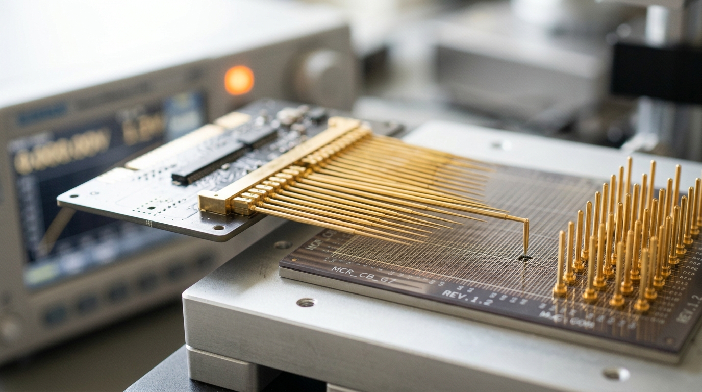
The multiplication step follows directly from two textbook circuit laws. Apply a voltage V_i simultaneously to each row i, representing the i-th component of an input vector. By Ohm’s law, the cell at row i and column j draws a current V_i times its conductance G_ij. By Kirchhoff’s current law, every current flowing into a given column sums automatically on that column’s wire, so the total current collected at the bottom of column j is
which is precisely the j-th component of the matrix-vector product between the input vector and the conductance matrix stored across the array — computed in one step, in parallel across every cell, using nothing but the physics of the wires and the stored conductances rather than a clocked multiply-accumulate circuit stepping through the same product one term at a time [6]. Because the weight is stored and multiplied in the same physical cell, it never has to be fetched from anywhere else to be used — the specific and narrow sense in which this design avoids the von Neumann bottleneck, distinct from the neuromorphic case above, which brings memory near to compute per core but still executes each multiplication as a discrete digital step.
Yao and colleagues built and tested a chip along exactly these lines: eight memristor crossbar arrays of 2,048 cells each, with each array functioning as a dedicated, fixed weight store for one layer of a five-layer convolutional network. Input image patches were applied sequentially as row voltage pulses, and the resulting output currents, accumulated on the column lines as described above, were read out directly as the convolution’s dot products. The fully hardware-executed network reached better than 96 percent accuracy on MNIST digit recognition, and the authors report energy efficiency more than two orders of magnitude greater than that of contemporary graphics processing units performing the same inference task [7]. That comparison is the authors’ own, specific to one comparatively easy benchmark and one fixed network, and should not be read as a general multiplier applicable to arbitrary workloads.
The same paper is also candid about the cost side of the trade. No two memristor cells, even fabricated side by side on the same die, program to identical conductances for identical pulses, and a given cell’s conductance can drift with time, temperature, and read history. Yao and colleagues’ response was a hybrid training method that adapts a network’s weights to each array’s measured imperfections rather than assuming an idealized crossbar, and Xia and Yang’s broader review frames large-scale, high-yield memristive arrays as still an early-stage fabrication problem, most published results at the time being small arrays or simulations rather than large fabricated systems [6]. This variability is the memristor’s direct analogue of the fabrication errors that erode a photonic mesh’s fidelity, and of the precision ceiling McMahon describes for optical computing — three unrelated substrates converging on one open problem: doing arithmetic directly in physical hardware buys parallelism and locality, and charges for both in precision and repeatability.
What a parameterized quantum circuit actually does — and does not yet do
The three mechanisms above are all, in a specific sense, physical shortcuts around a classical bottleneck: light instead of clocked logic to save a multiply, an asynchronous threshold instead of continuous evaluation to save idle power, an analog conductance instead of a memory fetch to save a bus trip. Each device’s internal state, at any instant, is still in principle a definite set of classical numbers. A quantum circuit is different in kind. Its state during computation is not reducible to a definite classical value stored at each qubit, and the operations performed on it are unitary transformations of the entire joint state of all the qubits together.
For a machine-learning task, the near-term architecture almost universally used is the parameterized (or variational) quantum circuit, and its mechanism has four concrete steps. First, classical input data x is encoded into a quantum state by applying a data-dependent unitary V(x) to a fixed initial state — commonly done by rotating each qubit by an angle set from one feature of x, so the input vector is literally written into rotation angles. Second, an “ansatz” unitary U(θ) — a fixed sequence of parameterized single-qubit rotation gates and two-qubit entangling gates, repeated over several layers — is applied, where θ is now a set of continuously adjustable classical numbers rather than data. Third, an observable A is measured on the resulting state; because quantum measurement is probabilistic, this means running the identical circuit many times and using the statistics of the 0/1 outcomes to estimate an expectation value, which becomes a term in a classical cost function
compared against a training label. Fourth, a classical optimizer running on an ordinary computer reads the estimated cost, proposes an updated θ, and the loop repeats: the quantum processor acts as a subroutine called repeatedly from an otherwise classical training loop, not as a machine that runs the whole learning process by itself [8]. This hybrid structure exists specifically because it tolerates shallow, noisy circuits far better than a single long, fully quantum program would — which is exactly why it dominates near-term quantum machine learning.
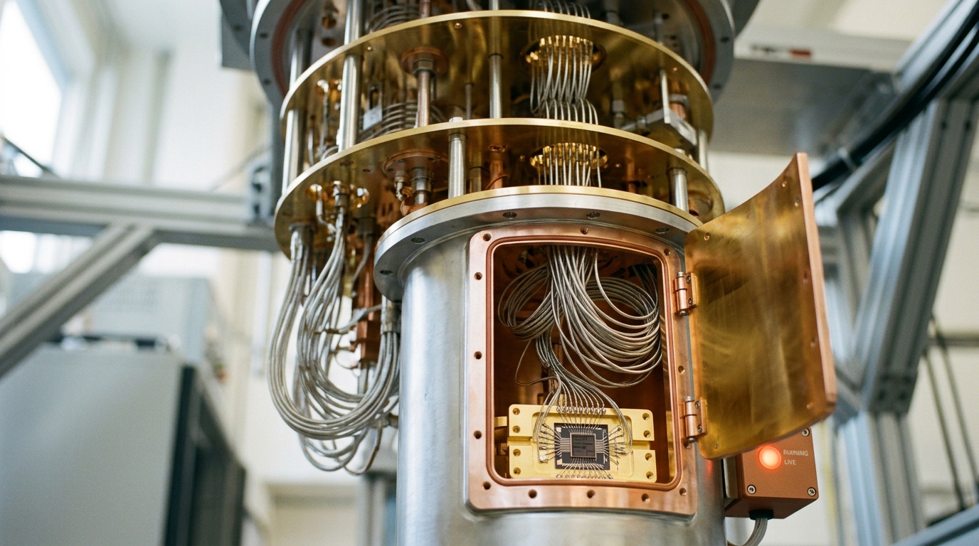
Two separate limits bound what circuits of this kind can actually do, and it matters that they are separate. The first is algorithmic rather than physical: for broad and important classes of ansatz, the variance of the cost function’s gradient with respect to θ shrinks exponentially as the number of qubits grows, a phenomenon called a barren plateau. Past a fairly modest circuit size, the gradient signal a classical optimizer sees becomes indistinguishable from statistical noise, and training simply stalls — Cerezo and colleagues document this occurring even in specific structured problems, such as variational linear-system solvers, not only in generic random circuits [8]. This is a structural argument against treating “more qubits, deeper ansatz” as an automatically better strategy for quantum machine learning, independent of anything the hardware does.
The second limit is physical: hardware noise and finite coherence time. Preskill’s 2018 framing of the current “noisy intermediate-scale quantum” (NISQ) era remains the field’s working reference point — noisy gates mean that circuit depth, not qubit count alone, is what actually bounds what a device can run reliably, and Preskill was explicit that a fifty-to-hundred-qubit noisy device, on its own, “will not change the world right away” [9].
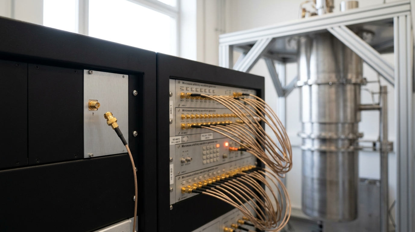
It is worth being concrete about what “today” actually means on deployed hardware, rather than leaving the number unstated. IBM’s newest superconducting processor, Nighthawk, entered early access in January 2026 with 120 qubits arranged on a square lattice and 218 tunable couplers, a measured median energy-relaxation time (T1) of roughly 350 microseconds, and a specification supporting circuits of up to about 5,000 two-qubit gates, against a published roadmap targeting 7,500 gates by the end of 2026 and 10,000 in 2027; the still-deployed Heron-generation ibm_boston processor runs 100 qubits at a typical two-qubit error rate near 2.15 times ten to the minus three [11]. Those are vendor-reported operating figures for currently accessible cloud hardware, not independently reproduced benchmarks, and they are cited here only to fix a scale: current parameterized-circuit experiments run on machines with, at most, a few hundred physical qubits and circuits of at most a few thousand gates — not the millions of qubits that appear in some popular accounts of the field.
The gap between that and a fault-tolerant machine is measured precisely by the best current error-correction result. Google’s Quantum AI group, on its 105-qubit Willow chip, built a distance-7 surface-code logical qubit from 101 physical qubits whose logical error rate came in below that of the single best physical qubit on the same device by a factor of 2.4, with each two-step increase in code distance suppressing the logical error rate by a further factor of about 2.14, reaching roughly 0.143 percent logical error per correction cycle at distance 7 [10]. That is a genuine, peer-reviewed first: operating “below threshold” means adding more physical qubits to the code reduces its logical error rate rather than adding more noise than it removes, the condition a scalable error-corrected machine requires. It is also a precise measure of the overhead still standing in the way — one adequately reliable logical qubit consumed 101 of the chip’s 105 physical qubits, on a device built specifically for this one experiment. A useful fault-tolerant algorithm needs many such logical qubits at a comparable tax, which is exactly why every current parameterized-circuit demonstration instead runs directly on noisy physical qubits with no error correction, accepting the noise rather than paying an overhead the field cannot yet afford.
Put the two limits together and the honest description of “quantum machine learning” in 2026 is narrow on both sides. What actually runs is small — tens to a few hundred qubits — shallow and uncorrected, chosen partly because the problem structure is believed less prone to a barren plateau and partly because it fits the coherence budget current hardware provides. What remains theoretical is a large-scale fault-tolerant algorithm with a rigorous advantage over the best classical method, which by the device numbers above needs logical qubit counts and correction overheads no existing machine is close to providing.
Four different physics, one shared trade
Set side by side, the four mechanisms share a structure even though nothing about their physics does. Each buys a specific, real advantage — parallel, passive computation from optical interference; near-zero idle power from event-driven spiking; collocated memory and arithmetic from analog conductance; access to a genuinely larger state space from superposition and entanglement — and each pays for it with a specific, real cost: an optical-to-electrical conversion tax and a roughly ten-bit precision ceiling for photonics; a workload-dependent payoff that requires remapping conventional networks onto an unfamiliar event-driven substrate for neuromorphic chips; device-to-device variability and drift that has to be actively compensated for memristors; and a severe qubit-count tax for reliability, plus a distinct algorithmic barrier in barren plateaus, for quantum circuits.
None of the specific efficiency or accuracy numbers cited above should be read as a comparison across substrates: each was measured by its own authors, on its own hardware and workload, and none has been independently reproduced head to head against the others or against a current GPU under matched conditions. That comparison, and what any of these four is actually good for in production, is deliberately outside the scope of this piece. What this article set out to establish is narrower and more load-bearing for a reader trying to evaluate a claim about any of these technologies: the specific circuit that does the arithmetic, and the specific physical reason it is claimed to be worth the trouble.