A parallel current, older than the mainstream it now shadows
Almost every AI system running today executes on the same underlying substrate: CMOS digital logic, arranged into GPUs and their accelerator cousins, multiplying matrices in fixed-point or floating-point arithmetic. That dominance feels inevitable from inside 2026, but it is a historical outcome, not a law of nature, and it is not even the oldest continuously pursued approach to building machines that compute the way brains, light, or quantum systems do. A separate research current — spanning analogue neuromorphic circuits, memristive devices, optical processors, and quantum hardware applied to learning — has been running for decades, in several cases predating the deep-learning boom itself by twenty or thirty years.
This article is a history, not a buyer’s guide. It traces four lineages from their documented origins to their current frontier, and it holds each claim to a single standard: a dated source that can be checked. Four threads recur across all of them. Each substrate began with a specific, nameable act of invention — a paper, a chip, a demonstration — rather than a vague gesture at “alternative computing.” Each then passed through a long gap between principle and working hardware, measured in decades rather than product cycles. Each was shaped as much by what defeated its first attempt as by what its founders originally proposed. And each remains, as of this writing, a research or early-commercial technology running alongside the CMOS mainstream rather than replacing any meaningful share of it. None of that is a prediction about what happens next; it is a description of what the record already shows.
Carver Mead and the invention of neuromorphic engineering
The word “neuromorphic” has a specific, checkable origin. Carver Mead, then a professor of engineering and applied science at the California Institute of Technology, used it in a 1990 paper in the Proceedings of the IEEE titled “Neuromorphic Electronic Systems,” which argued that biological information processing achieves its efficiency not by computing faster than silicon but by using elementary physical phenomena — the exponential current-voltage relationship of a transistor operating below threshold, for instance — as computational primitives in their own right, and by representing information as relative analogue signal values rather than discrete digital ones [1].
That 1990 paper formalized a research program that had already been running at Caltech for several years. According to Caltech’s own account, the university established the world’s first graduate program in computation and neural systems in 1986, and Mead published the field-defining textbook Analog VLSI and Neural Systems in 1989 — both concrete, dated markers that predate the paper that named the field [2]. The method itself was not abstract theorizing: Mead’s group built physical analogue chips — silicon retinas and related sensory circuits — that computed with the same subthreshold-transistor physics a biological neuron’s membrane uses, rather than simulating neurons numerically on a general-purpose digital processor.
Credit for that work is not solely Mead’s, and the historical record is explicit about this. Caltech’s own retrospective quotes Mead crediting his graduate student Misha Mahowald directly: the silicon retina, he said, “was Misha’s idea, and she basically dragged me into neurobiology… She was the one who started this field, and I was fortunate to partner with her in the process” [2]. The prize that now recognizes lifetime contributions to the field Mead is credited with naming carries Mahowald’s name, not his — a detail that matters for any accurate account of neuromorphic engineering’s origin, because it correctly distributes credit between the person who articulated the program in print and the person whose specific circuit ideas made it concrete.
What made this work “post-CMOS” in spirit even though it was built in CMOS silicon is worth being precise about. Mead’s chips were not digital simulations of neurons running on conventional logic; they used the transistor’s own analogue physics as the computational element, sidestepping the instruction-fetch-decode-execute cycle of a von Neumann machine entirely. That distinction — computing with device physics directly rather than simulating a model of it in software — is the thread that connects Mead’s 1980s silicon retinas to the digital-but-still-neuromorphic chips built decades later, and it is worth holding in mind through the rest of this history, because every subsequent lineage in this article makes a version of the same bet: that some physical substrate, if used honestly rather than simulated, computes a class of problems more directly than a general-purpose digital processor does.
A circuit element predicted, then found thirty-seven years later
Two years before Mead’s Caltech program formalized, and nineteen years before he named the field it eventually became part of, a circuit theorist at Berkeley had already predicted the existence of a device neuromorphic and AI hardware would later depend on.
In 1971, Leon Chua published “Memristor — The Missing Circuit Element” in IEEE Transactions on Circuit Theory. His argument was one of pure symmetry, not empirical discovery. Circuit theory recognizes four fundamental variables — charge, current, voltage, and magnetic flux linkage — and, in 1971, three of the six possible pairwise relationships among them were already embodied in named components: the resistor relates voltage and current, the capacitor relates charge and voltage, the inductor relates flux linkage and current. Chua noticed that the sixth relationship, between charge and flux linkage, had no corresponding physical device, and reasoned from the completeness of the other five that one should exist. He named the missing element the memristor and gave it a defining relation:
where
For thirty-seven years, the memristor remained exactly what Chua’s title said it was: missing. No one had built, or clearly identified, a physical device with that behavior. That changed in 2008, when Dmitri Strukov, Gregory Snider, Duncan Stewart, and R. Stanley Williams, working at HP Labs, published “The Missing Memristor Found” in Nature. They showed that memristance arises naturally in nanoscale systems where electronic and ionic transport are coupled under an applied bias — concretely, in thin titanium-dioxide films where an electric field can drag mobile oxygen vacancies through the material, continuously changing its resistance in a way that persists after the field is removed. The paper opens by directly crediting Chua’s 1971 reasoning and states plainly that “until now no one has presented either a useful physical model or an example of a memristor” [4].
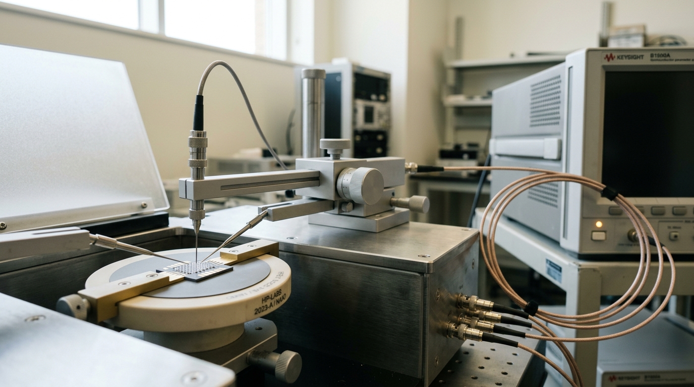
The AI relevance of that finding is direct rather than metaphorical: a memristor sitting at the crosspoint of a wire grid can store an analogue weight and perform a multiply-accumulate operation on the current passing through it in the same physical step, which is the operation a neural-network layer spends nearly all of its energy on when done digitally. That is the promise. The historical record through 2026, however, is more measured than the promise: memristive compute-in-memory remains largely a research and specialized-deployment technology rather than a mainstream alternative to CMOS accelerators, and the gap has as much to do with device-to-device and cycle-to-cycle variability at manufacturing scale as with the underlying physics, which is by now well characterized. That is an analytical judgment about where the technology currently sits, not a claim drawn from either source above, and it should be read as such — the two memristor sources establish the theory and the device; they do not themselves make claims about commercial maturity.
Light as the medium, and why the first attempt stalled
Optical computing is older than either of the two threads above, and its history has an unusually clean shape: a genuine early wave, a specific and well-understood failure, and — much later — a narrower, more defensible second attempt that is still playing out.
A 2022 review in Nanomaterials, “Optical Computing: Status and Perspectives,” traces the field’s origins to the early 1960s, when military-driven interest in Fourier-transform optics motivated coherent optical systems for image processing and pattern recognition. Enthusiasm sharpened considerably in the early 1980s around a more ambitious goal: using nonlinear optical materials to implement the basic Boolean logic functions — AND, OR, NAND, NOR — directly in light, which raised the prospect of computers built from cascades of optical logic gates operating at the speed of light with none of a wire’s parasitic capacitance [5].
That first wave did not fail for a single reason, and the review is specific about the combination that defeated it. Available optical nonlinearities were weak, which made efficient, low-loss optical logic gates difficult to build; no practical form of optical memory existed, which is a serious problem for a computer, since a machine that cannot hold a bit between operations cannot easily chain them; and every stage inserted into a cascaded optical system compounded signal loss and demanded increasingly precise alignment, an engineering burden that grew faster than the systems it was meant to build. Meanwhile, the competing substrate kept improving on its own schedule: the review notes that “silicon digital electronic processing appears to have nearly always been chosen for final manufacturing equipment” once systems reached the point of needing to actually ship, because electronics’ reliability and manufacturing maturity consistently outweighed optics’ theoretical speed advantage [5]. CMOS scaling through the 1980s and 1990s did not just compete with optical computing — it moved the goalposts every eighteen months, a pace no less-mature optical technology stack could match while also solving the logic-gate and memory problems from a standing start.
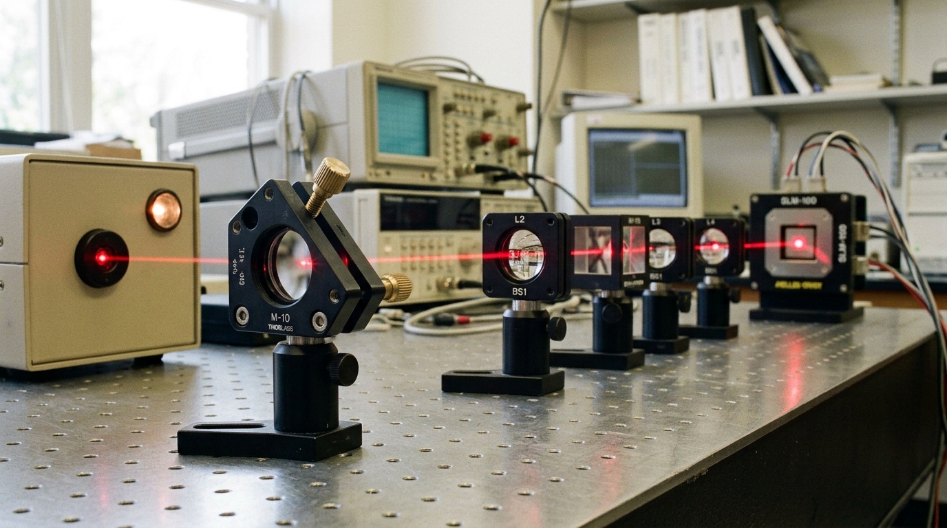
The lesson the field eventually drew from that failure, discussed later in this article, was not “optics cannot compute” but “optics should not try to do everything.” The general-purpose optical logic computer — light performing Boolean operations end to end, including memory — is the specific ambition that stalled. A narrower reformulation, restricted to the one operation optics performs with genuine physical efficiency, would not resurface as a serious commercial pursuit for roughly another quarter-century.
Quantum algorithms before “quantum machine learning” had a name
Quantum computing’s relationship to machine learning did not begin with an algorithm called “quantum machine learning.” It began with an algorithm for a much narrower, more classical-sounding problem, and the connection to learning was drawn afterward.
In 2009, Aram Harrow, Avinatan Hassidim, and Seth Lloyd published “Quantum Algorithm for Linear Systems of Equations” in Physical Review Letters. The problem they addressed — given a system
The field acquired that explicit label, and a systematic accounting of what it did and did not yet support, in 2017. Jacob Biamonte, Peter Wittek, Nicola Pancotti, Patrick Rebentrost, Nathan Wiebe, and Seth Lloyd published “Quantum Machine Learning” as a review in Nature, surveying quantum algorithms proposed as building blocks for learning systems and stating the field’s central, still-unresolved bet plainly: that quantum systems can produce statistical patterns classical systems are believed not to reproduce efficiently. The review’s own framing of the gap between proposal and hardware is unambiguous — it describes algorithms that “could act as the building blocks of machine learning programs” while noting that “the hardware and software challenges are still considerable” [8].
That hardware gap acquired its own name the following year. In 2018, John Preskill published “Quantum Computing in the NISQ Era and Beyond” in the journal Quantum, coining the term NISQ — noisy intermediate-scale quantum — for the generation of devices then coming online: quantum processors with roughly 50 to 100 qubits, too small and too error-prone for fault-tolerant computation, but potentially large enough to explore problems classical computers struggle with. Preskill’s own summary of the moment doubled as a corrective to hype building around it: “the 100-qubit quantum computer will not change the world right away,” he wrote, framing NISQ devices instead as tools for exploring quantum many-body physics and “other useful applications,” and as a step toward — not a substitute for — fully fault-tolerant quantum computing [7].
The reason NISQ-era hardware imposes such a hard ceiling on quantum machine learning specifically is a simple compounding effect. If a device executes a circuit of
which decays exponentially in circuit depth for any fixed error rate
Neuromorphic engineering reaches wafer scale
While memristors, optics, and quantum hardware were each working through their own founding constraints, the neuromorphic thread Mead had named in 1990 spent the following two-plus decades moving from small analogue research chips toward digital, wafer-scale systems built specifically to run at the size a real workload requires.
The clearest marker of that transition arrived on August 7, 2014, when IBM, working with Cornell Tech under DARPA’s SyNAPSE program, announced TrueNorth: a single chip carrying 5.4 billion transistors, implementing one million programmable spiking neurons and 256 million programmable synapses, and consuming approximately 70 milliwatts of power — several orders of magnitude below what a conventional processor of comparable transistor count would draw. The underlying research, “A Million Spiking-Neuron Integrated Circuit with a Scalable Communication Network and Interface” by Paul Merolla and collaborators, appeared in Science the following day, and the specifications above are corroborated in contemporaneous technical reporting on the announcement [9]. TrueNorth’s architecture broke deliberately from the von Neumann model Mead’s original silicon retinas had also sidestepped: computation, memory, and communication were distributed across a tiled array of 4,096 neurosynaptic cores rather than centralized around a shared bus, with an event-driven, asynchronous design that consumes power only when a spike actually occurs.
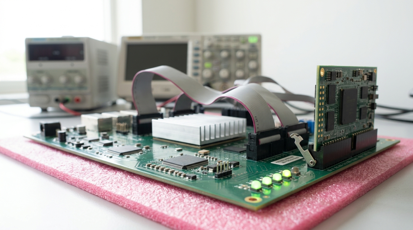
Intel entered the same silicon lineage three years later. On September 25, 2017, Intel announced Loihi, a research chip fabricated on its 14-nanometer process, carrying 128 neuromorphic cores that together implement roughly 130,000 neurons and 130 million synapses. Intel’s own announcement framed the target application directly — machines that “self-organize and make decisions based on patterns and associations” while operating in real time rather than depending on cloud connectivity — and claimed up to 1,000 times better energy efficiency than general-purpose computing on the kind of continual, online learning tasks Loihi was built for [11]. Contemporaneous reporting on the announcement adds a detail that captures the chip’s specific technical claim well: Intel researcher Narayan Srinivasa noted that “the brain doesn’t communicate as often as you’d think. This chip doesn’t consume energy until there’s a spike” [12]. The peer-reviewed account of the architecture, “Loihi: A Neuromorphic Manycore Processor with On-Chip Learning” by Mike Davies and 21 co-authors, was published in IEEE Micro in 2018 and documents Loihi’s central innovation: a microcode-based learning-rule engine embedded in each neural core, giving the chip fully programmable, on-chip synaptic plasticity rather than fixed, pre-trained weights loaded from outside [10].
Intel followed with a second generation on September 30, 2021. Loihi 2, fabricated on a pre-production Intel 4 process using extreme-ultraviolet lithography, scaled to up to one million neurons per chip, delivered up to ten times faster processing and up to fifteen times greater resource density than the original Loihi, and shipped alongside Lava, an open-source software framework Intel released specifically because the neuromorphic research community lacked a common programming model spanning conventional and neuromorphic hardware [13]. That software detail is not incidental to this history: a novel compute substrate without a shared software stack cannot accumulate an ecosystem of workloads mapped onto it, and Lava’s release marks the point at which Intel’s neuromorphic line began treating that gap as a first-class problem rather than an afterthought.
Photonics, reopened around a narrower bet
The optical-computing wave that stalled in the 1990s did not disappear so much as go quiet for a generation, waiting for a version of the idea narrow enough to actually work. That version arrived in 2017, from a different direction than the original attempt.
Where the 1980s program had tried to build general-purpose optical logic — including optical memory, the piece that proved hardest to solve — a team including Yichen Shen, Nicholas Harris, Dirk Englund, and Marin Soljačić published “Deep Learning with Coherent Nanophotonic Circuits” in Nature Photonics in 2017, restricted to a single, much more tractable operation: matrix multiplication, the arithmetic operation that dominates a neural network’s inference cost. Their prototype used a cascaded array of 56 programmable Mach-Zehnder interferometers etched into a silicon photonic integrated circuit, physically implementing a learned linear transformation as light propagated through the mesh, and demonstrated the approach on a vowel-recognition task [14]. The strategic shift is the important part: by keeping nonlinearity and memory in conventional electronics and asking optics to do only the linear-algebra step it performs with genuine physical efficiency, the 2017 approach sidestepped exactly the two problems — weak optical nonlinearity and absent optical memory — that had defeated the field’s first attempt.
That academic reopening turned into a sustained commercial pursuit within a few years, led in part by one of the 2017 paper’s own co-authors. Nicholas Harris went on to found Lightmatter, a company built specifically around photonic AI hardware. In March 2025, Lightmatter announced Passage L200 and Passage M1000, co-packaged optical interconnect products aimed at the bandwidth bottleneck between AI accelerators in a datacenter rather than at the matrix-multiply core itself — a distinct but related bet that photonics’ advantage in AI infrastructure may arrive first through interconnect, where the physics is less demanding, even as photonic compute continues to mature [16].
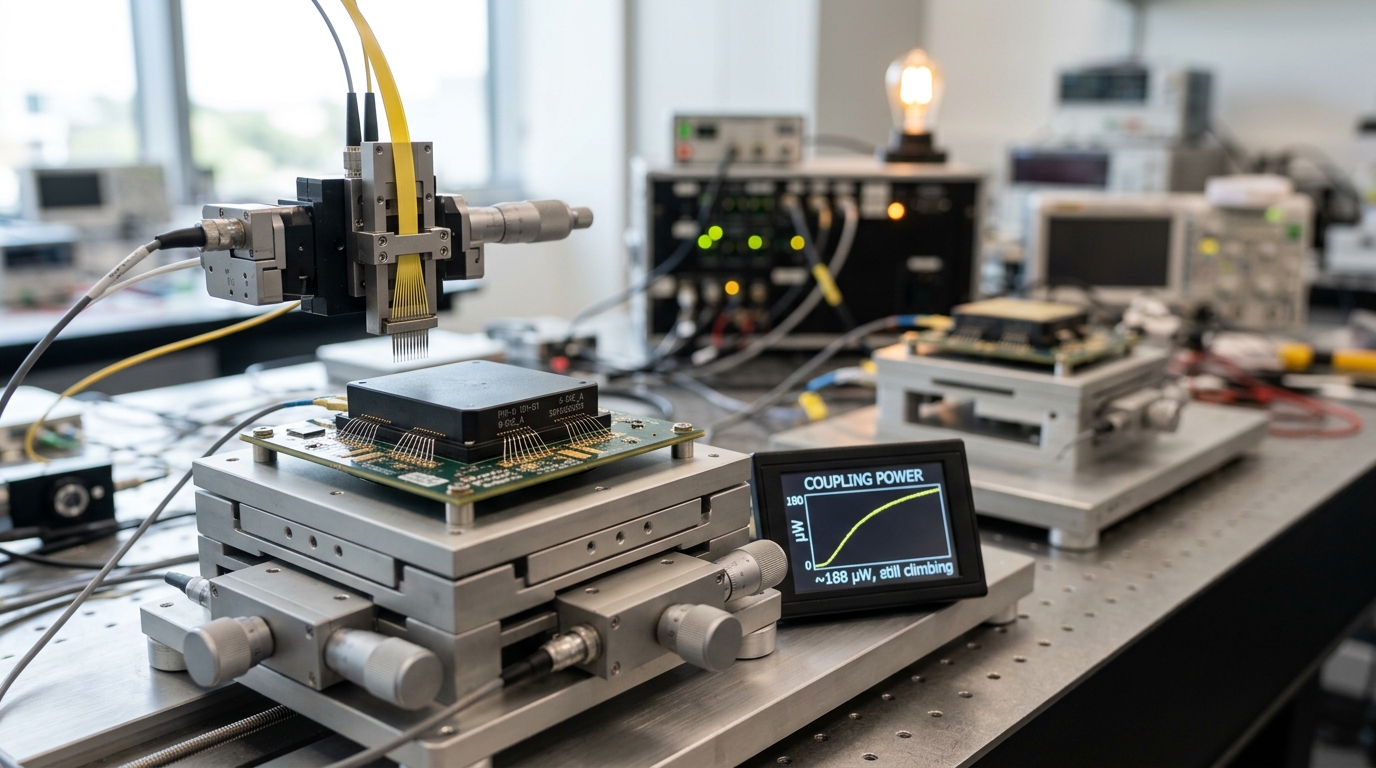
The compute core reached a genuine milestone the following month. In April 2025, Sufi Ahmed, Reza Baghdadi, and more than forty co-authors from Lightmatter and OpenAI published “Universal Photonic Artificial Intelligence Acceleration” in Nature, describing a photonic processor built from four 128-by-128 photonic tensor cores spread across six packaged chips. The system executed several established neural-network benchmarks — the ResNet image classifier, the BERT language model, and the Atari deep-reinforcement-learning algorithm originally demonstrated by DeepMind — without modifying the models to accommodate the hardware, reaching accuracy close to that of conventional digital processors while sustaining 65.5 trillion adaptive block floating-point operations per second on roughly 78 watts of electrical power and 1.6 watts of optical power [15]. That “without modification” detail is the specific bar the 1990s wave never cleared: earlier optical demonstrations typically required a problem simplified to fit the optics, where the 2025 result ran standard models used elsewhere in the field, unaltered.
What five decades of alternatives actually show
Laid end to end, these four histories share a structure that is easy to miss when each is told in isolation. Every one of them began with a specific, dated act — a named paper, a named chip, a named demonstration — not a vague research trend, and every one of them then spent a long interval, measured in decades, between that founding act and hardware that worked at any meaningful scale. Chua’s prediction took thirty-seven years to become Strukov and colleagues’ titanium-dioxide device. Mead’s 1990 naming of neuromorphic engineering sits twenty-four years before TrueNorth and thirty-one before Loihi 2. The first optical-computing wave ran roughly two decades before its narrower, more defensible successor began in 2017. Quantum machine learning is the youngest of the four threads by a wide margin, and its own leading theorist was explicit in 2018 that the hardware of the moment would not, on its own, change the world.
It would be a mistake to read that pattern as evidence any of these substrates is close to displacing CMOS digital accelerators for general AI workloads — none of the sources above make that claim, and this article does not either. It would be an equally serious mistake to read the pattern as evidence the opposite: that none of them matter. TrueNorth and the Loihi line are shipping, programmable neuromorphic silicon with a real software stack around them. Memristive crossbars are a well-characterized physical mechanism, even where manufacturing variability remains a genuine open problem rather than a solved one. Photonic accelerators went, within eight years of the field’s academic reopening, from a 56-interferometer laboratory demonstration to a chip running unmodified production-scale models at close to electronic accuracy. And NISQ-era quantum hardware is, by its own leading advocate’s account, a real step on a longer road rather than a finished destination.
Where practitioners inside each of these four camps disagree — and they do, sometimes sharply, about which substrate is closest to a broadly useful commercial threshold — this article deliberately does not adjudicate. The honest summary the historical record supports is narrower and more useful than a ranking: four separate, real engineering lineages, each still short of the mainstream, each currently being pushed forward by named researchers and named companies whose specific, dated claims can be checked one at a time. That is what “post-CMOS” compute has actually been, from Mead’s late-1980s Caltech bench to a 2025 photonic chip built with OpenAI — not a single frontier, but several, advancing at their own separate rates.