Four lineages, one collision course
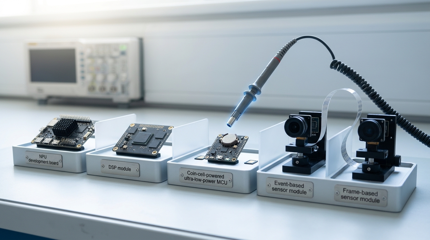
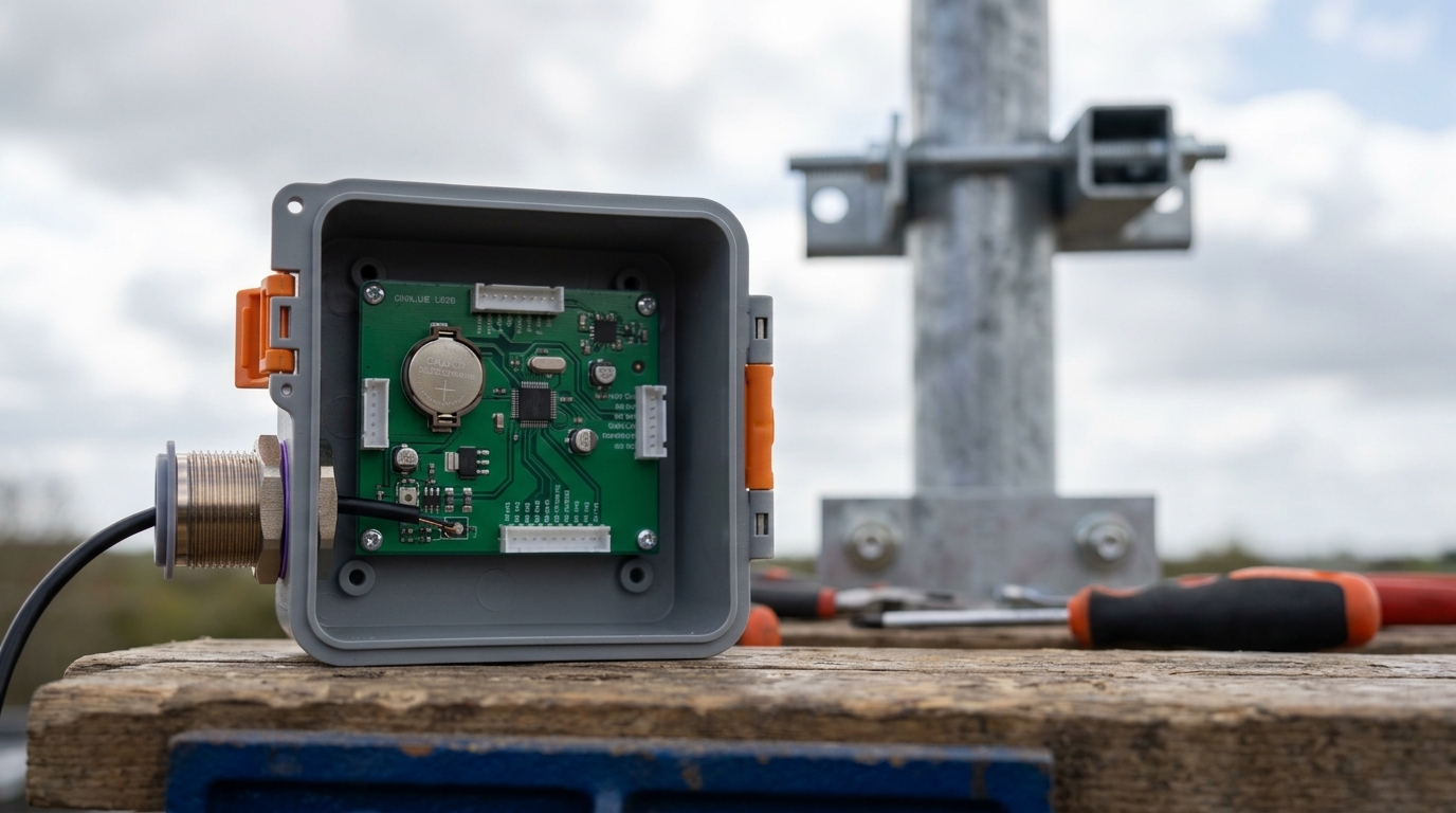
“Edge AI” reads as a single recent invention — the smartphone that recognises a face without calling home, the doorbell camera that tells a person from a passing car. Treated that way, the history is short and starts around 2017. Treated honestly, it is the convergence of four hardware lineages that developed mostly independently for decades before anyone had reason to put them in one sentence: general-purpose embedded microcontrollers, which learned to fit a whole computer on one chip; MEMS sensors, which learned to manufacture a mechanical measuring instrument out of silicon; neuromorphic and event-based vision, which asked what a camera would look like if it worked more like a retina; and dedicated neural processing hardware, which arrived last and only because the other three had already made a phone worth putting one inside. This article follows each lineage from its dated origin, marks the points where they meet, and ends with a reminder that a hardware history is not complete without its commercial failures alongside its technical successes.
Two threads run under all four. First, every one of these devices has had to solve the same architectural problem regardless of decade: how much of the signal chain — sensing, analog conditioning, and decision — can be pulled onto or next to a single die, because every stage left off-chip costs power, latency, and reliability. Second, every one of them has had to answer the same question about where computation should happen at all: on the sensor, in a nearby microcontroller, or somewhere else entirely — a question with direct consequences for privacy and for how fast a system can close a control loop, not only for cost.
1974: a computer that fit on one chip, built for a calculator
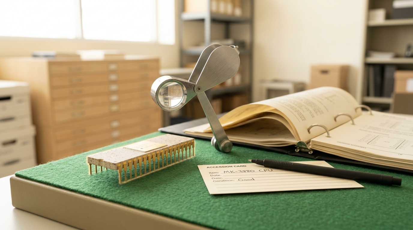
The lineage that eventually produces every microcontroller inside a modern sensor node starts with a chip designed to do arithmetic, not control anything. Gary Boone and Michael Cochran’s 1971 single-chip calculator design at Texas Instruments, the TMS1802, supplied the template that TI generalised into the TMS1000 family, announced in 1974 as a complete “computer on a chip” combining a 4-bit CPU, ROM, RAM, and I/O lines on one die, according to the Computer History Museum’s account of the announcement [1]. What made the TMS1000 historically significant was not its arithmetic, which was modest, but its price and its generality: at $2 in volume, it was cheap enough to embed in products that had never before contained a programmable computer at all — burglar alarms, garage door openers, and toys, most famously Speak & Spell, which the Computer History Museum credits with introducing digital electronics to ordinary consumers [1].
That is the shape the whole microcontroller lineage repeats: a general-purpose computer, cheap and small enough to disappear into a product that is not itself a computer. Six years later, Intel’s 8051 pushed the same idea further. Introduced in 1980 as the flagship of the MCS-51 family, the 8051 combined an 8-bit CPU, 4 kilobytes of program ROM, 128 bytes of RAM, two timers, a serial port, and 32 digital I/O lines on a single 40-pin package, and could run programs up to sixteen times larger than Intel’s earlier 8048, according to Intel’s own retrospective account of the chip [2]. The 8051 was not the first microcontroller — that credit belongs to the TMS1000 lineage — but Intel’s account states plainly that it became the first to see truly widespread, lasting use: Intel sold 100 million MCS-51 units in the chip’s first decade, and the architecture “essentially set a world standard” that enhanced, binary-compatible derivatives from other manufacturers still ship today [2]. Every sensor node built since — every device with a microcontroller reading an analog-to-digital converter, running a control loop, and reporting a result — inherits its basic shape from a lineage that began as a way to make a $2 calculator chip do something else.
1991: sensing becomes a manufactured part, not an assembled instrument
Mechanical sensing had existed for as long as engineering had, but it required an assembled instrument: springs, masses, and mechanical linkages built and calibrated as discrete parts. MEMS — micro-electromechanical systems — changed the unit of manufacture from an assembled instrument to a single chip, and the accelerometer was the device that proved the idea could be sold at volume. Analog Devices introduced the ADXL50 in 1991 as, by the company’s own account, the first surface-micromachined monolithic accelerometer put into commercial, high-volume production, a complete measurement system on one chip combining a differential capacitive polysilicon sensing element with signal-conditioning circuitry and a built-in self-test feature, all on a single die [3]. The self-test capability mattered as much as the sensing itself: it let automakers verify, electrically and without a mechanical shake table, that the part was still working after it had been soldered onto a board — a prerequisite for trusting an unfamiliar silicon sensor with the job of deciding, in milliseconds, whether to fire an airbag. Analog Devices priced the ADXL50 at roughly a quarter of what the mechanical crash sensors it displaced had cost, and the company’s own materials describe the part as having opened the door to MEMS sensors across the rest of the automotive industry [3].
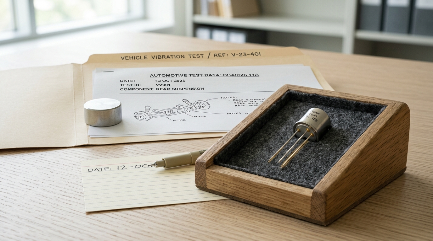
The ADXL50 is a useful case study in why “edge electronics” and “analog front end” are not separable ideas. A bare micromachined capacitive element produces a signal measured in femtofarads — far too small and far too noisy to hand directly to a digital system. What made the ADXL50 a product rather than a laboratory demonstration was putting the amplification, filtering, and self-test circuitry for that signal on the same piece of silicon as the sensing structure itself, so that the part leaving the factory was already a complete, calibratable measurement chain rather than a fragile transducer requiring careful external circuit design by every customer. That pattern — mechanical or optical sensing element, integrated analog front end, and a digital interface, all on one die or one package — is the template every MEMS gyroscope, MEMS microphone, and, later, every event-camera pixel would follow.
1988–1991: a photoreceptor that reports change, not brightness
While MEMS sensing was proving itself in Detroit’s supply chain, a separate and much stranger research program was underway at Caltech, asking a different question entirely: not how to manufacture a sensor cheaply, but how to build a sensor that computed the way biological vision does. Carver Mead’s neuromorphic engineering group, working with graduate student Misha Mahowald, built an analog VLSI chip designed to model the outer retina’s early visual processing rather than simply capturing an image. Their 1991 Scientific American paper, “The Silicon Retina,” describes a chip with an adaptive photoreceptor circuit that responds with high gain to small spatial and temporal changes in light intensity, extending the effective dynamic range of the receptor well beyond what a fixed-gain photodiode could achieve, and doing so using the same kind of subthreshold analog circuit techniques Mead had developed for neuromorphic computation generally [4]. The paper’s central move — treating a pixel as a circuit that computes a local temporal contrast rather than as a device that merely reports absolute brightness — is the conceptual ancestor of every event camera built since, even though it would be nearly two decades before that idea reached a commercial product.
2008: the sensor that made “event camera” a hardware category
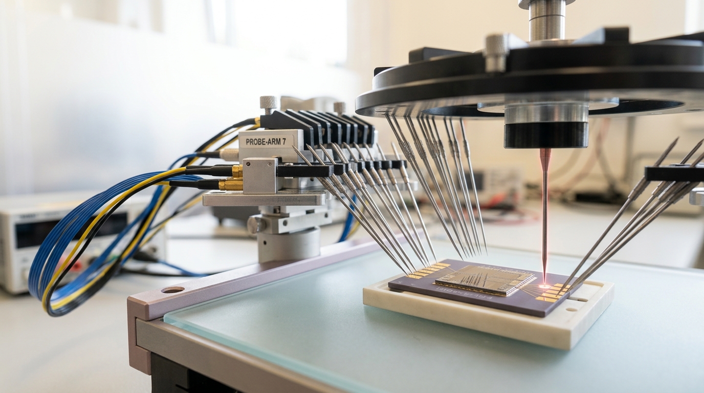
The silicon retina was a research demonstration; the modern event-camera sensor is an engineering result with a specific, dated, peer-reviewed origin. In 2008, Patrick Lichtsteiner, Christoph Posch, and Tobi Delbruck published a paper in the IEEE Journal of Solid-State Circuits describing a 128×128-pixel CMOS vision sensor in which every pixel independently and continuously quantises local relative changes in light intensity, generating an asynchronous stream of address-events rather than a sequence of full frames, with a reported dynamic range of 120 decibels and 15-microsecond latency [5]. The paper’s own framing of the result is worth quoting directly, because it states the efficiency argument that motivates every subsequent event-camera product: the sensor’s output data rate depends on the dynamic content of the scene rather than on a fixed frame rate, and is “typically orders of magnitude lower than those of conventional frame-based imagers” for scenes that are mostly static [5]. That is a power and bandwidth argument as much as a vision-science one — a sensor that only reports what changed does not have to move, store, or process data describing what did not, which is exactly the property that later made event sensors attractive for battery-powered and always-on edge devices rather than only for laboratory neuroscience.
The device that paper describes, generally known by its research name DVS128, did not become a commercial product on its own. It became one through a company.
2014–2020: event vision becomes a company, then a co-developed chip
Prophesee, originally named Chronocam, was founded in 2014 within the iBionext start-up studio in Paris by Ryad Benosman, Bernard Gilly, Christoph Posch — a co-author of the 2008 DVS128 paper — and Luca Verre, combining experience in image sensing, neuromorphic computing, and VLSI design with the explicit goal of commercialising event-based vision [6]. The company renamed itself Prophesee in 2018 and spent the following years building both its own event-sensor products and partnerships with established imaging manufacturers, a strategy that culminated in February 2020 with a jointly developed sensor announced with Sony at the International Solid-State Circuits Conference: a stacked event-based vision sensor combining Sony’s CMOS stacking process with Prophesee’s Metavision pixel technology, claimed at the time to have the industry’s smallest event-sensor pixel at 4.86 micrometres, a 1280×720 resolution, greater than 77 percent fill factor, a maximum event rate above one billion events per second, one-microsecond timestamp resolution, and roughly 73 milliwatts of power draw at a 300-million-event-per-second rate [12]. Whatever one makes of “industry’s smallest” as a marketing claim — it is Prophesee’s own characterisation, not an independent benchmark — the underlying engineering fact is not in dispute: stacking let the event-sensing pixel array and its digital readout circuitry sit on separate, independently optimised silicon layers bonded together, the same die-stacking approach conventional CMOS image sensors had already adopted to shrink pixel pitch, applied here to a fundamentally different pixel that reports contrast changes instead of exposure levels.
September 2017: two companies announce a “first” ten days apart
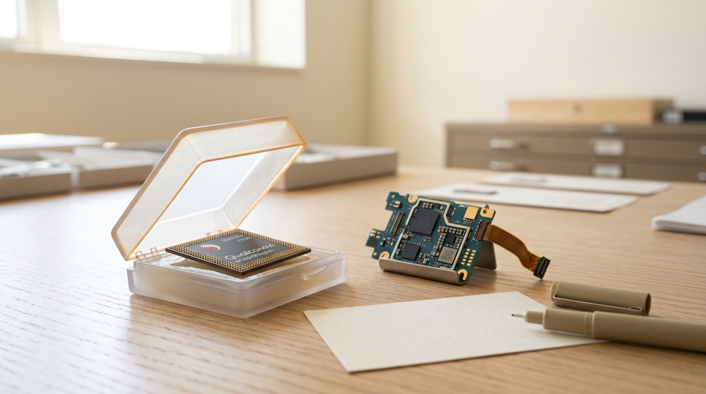
Dedicated neural processing hardware reached consumer smartphones in a compressed and, in retrospect, slightly awkward two weeks. On September 2, 2017, at IFA in Berlin, Huawei’s Consumer Business Group unveiled the Kirin 970 chipset, describing it as containing a dedicated Neural Processing Unit as part of what Huawei’s own press materials called its “first mobile AI computing platform,” built on a 10-nanometre process with 5.5 billion transistors and claimed, by Huawei, to deliver up to 25 times the performance and 50 times the efficiency of a comparable general-purpose CPU cluster on machine-learning workloads [7]. Ten days later, on September 12, 2017, Apple announced the A11 Bionic chip inside the iPhone X, iPhone 8, and iPhone 8 Plus, built around a dual-core Neural Engine capable of up to 600 billion operations per second and used, according to Apple’s own announcement, to power on-device Face ID authentication and Animoji rather than being framed by Apple as a general-purpose “NPU” brand at all [8].
Both companies have, in their own materials, described their September 2017 chip as a first of its kind — Huawei explicitly for a dedicated smartphone NPU, Apple implicitly through the Neural Engine’s marketing as a new category of on-device silicon. These are vendor claims made about overlapping but not identical things — Huawei’s framing centres a named, general-purpose accelerator block; Apple’s centres a specific, named engine tied initially to particular first-party features — and reconciling exactly who shipped “first” requires deciding which claim about which chip should count, a question this article does not attempt to settle. What is not in dispute is the underlying architectural shift both chips represent: before 2017, machine-learning inference on a phone ran on general-purpose CPU or GPU cores; after 2017, flagship mobile system-on-chips routinely shipped a separate block of silicon designed specifically for the matrix-multiply-heavy arithmetic of neural network inference, alongside the CPU and GPU rather than instead of them.
That architectural shift had a consequence beyond speed. Apple’s own privacy documentation for Face ID states that facial recognition data, including the mathematical representations of a user’s face, “does not leave your device, and is never backed up to iCloud or anywhere else,” and is instead encrypted and protected by keys available only to a secure hardware enclave on the device itself [9]. That guarantee is only possible because there is enough dedicated silicon on the phone to run the recognition model locally in real time; a system that had to send a camera image to a server to get an authentication decision back could not make the same claim, regardless of what encryption it used in transit. Dedicated on-device neural silicon is, among other things, a privacy architecture decision made at the hardware layer, years before any policy document describes it as one.
2019: a name arrives for a field that had been assembling itself for years
By 2019, all three of the preceding lineages — cheap embedded microcontrollers, integrated MEMS sensors, and increasingly efficient neural network inference — had matured to the point that running a small trained model directly on a battery-powered microcontroller, using nothing but the sensor and the chip already on the board, was becoming routine in research and in a scattering of shipping products. What that practice lacked was a name and a community organised around it. Pete Warden and Daniel Situnayake’s book “TinyML: Machine Learning with TensorFlow Lite on Arduino and Ultra-Low-Power Microcontrollers,” published by O’Reilly in December 2019, gave the field both, framing it explicitly around deep learning models compact enough to run on microcontrollers — citing, as one illustrative example, a keyword-detection model built by Google’s Assistant team small enough to fit in 14 kilobytes [10]. The book’s arrival coincided with, and helped organise, the founding of the tinyML Foundation and its first annual Summit, giving practitioners who had been working on the same problem in isolation — squeezing a useful model into a few hundred kilobytes of flash and a power budget measured in milliwatts — a shared vocabulary and a venue.

June 2021: the field agrees on how to measure itself
A named field without a shared benchmark cannot compare results across research groups or vendors, and TinyML’s practitioners spent roughly eighteen months building one. MLCommons, working with the Embedded Microprocessor Benchmark Consortium and more than twenty participating organisations including Harvard University, Google, Qualcomm, and STMicroelectronics, released the MLPerf Tiny Inference benchmark on June 16, 2021, designed specifically to measure the accuracy, latency, and — as an optional but explicitly supported measurement — the energy consumption of neural network inference on extremely low-power devices [11]. The suite’s four tasks — keyword spotting, visual wake words, image classification, and anomaly detection — were chosen because they map directly onto the sensing modalities edge AI hardware actually processes: a microphone listening for a wake word, a low-resolution camera checking whether a scene contains a person, a general image classifier, and a stream of sensor readings checked for anomalous patterns [11]. Making power measurement an explicit, optional part of a standardised benchmark — rather than an afterthought reported inconsistently by whichever team happened to measure it — is itself a marker of how central the power budget had become to the field’s definition of success: a TinyML model is not judged only on accuracy, but on accuracy achieved within a power envelope small enough for a device that may run for months on a coin cell.
2023–2025: convergence, and a reminder that hardware history includes failure
By the early 2020s, the four lineages this article has traced were no longer separate stories. A 2023 survey in IEEE Circuits and Systems Magazine by Ji Lin, Ligeng Zhu, Wei-Ming Chen, Wei-Chen Wang, and Song Han frames tiny machine learning explicitly as squeezing deep learning models onto the billions of microcontroller-class IoT devices already in the field, and demonstrates system-algorithm co-design techniques — the authors’ MCUNet work among them — aimed at running models with substantially larger effective capacity than a microcontroller’s memory would naively allow, by jointly optimising the neural network architecture and the inference system that runs it rather than treating the two as separable problems [13]. That co-design instinct — do not just shrink the model, redesign the whole chain from sensor to silicon to algorithm together — is the same instinct visible in the ADXL50’s integrated analog front end and in the event camera’s pixel-level contrast computation, applied now to neural network inference specifically.
Convergence, however, is not the same as commercial safety, and the record should not skip past that. Prophesee, whose 2008-lineage event sensors this article has followed from a research paper through a co-developed Sony product, filed for insolvency and entered judicial recovery in France in late 2024, after the company said its next fundraising round had taken longer to close than expected, despite having raised roughly 126 million euros across its history and having announced, only months earlier, that its sensor technology had become available in AMD’s vision AI products [14]. The company’s own leadership maintained at the time that the underlying technology remained sound and that operations continued while a rescue financing was arranged [14]. Whether or not any individual company survives, that gap between a technically validated sensor and a durable business built on it is a real feature of edge AI hardware history, not an incidental footnote to it: the TMS1000, the 8051, and the ADXL50 all reached the scale where a reader might reasonably forget any company involved in inventing them could have failed to commercialise them at all.
Predictions, with the observations that would falsify them
These are forecasts, clearly separated from the sourced history above. Horizon: 16 August 2029.
One. Power measurement will become a mandatory rather than optional part of edge-AI inference benchmarks, following the direction MLPerf Tiny already set by including it as an option in 2021. Disconfirmed if the leading benchmark suites for microcontroller-class inference in 2029 still report accuracy and latency without energy figures as the norm.
Two. The architectural convergence visible in MCUNet-style system-algorithm co-design will extend to sensor-algorithm co-design as standard practice, with event-camera and MEMS sensor output formats designed jointly with the tiny models that consume them rather than adapted afterward. Disconfirmed if by 2029 event-camera and MEMS sensor interfaces remain generic and unchanged by the neural inference workloads reading them.
Three. Consolidation among independent event-camera and neuromorphic-sensor startups will continue, with surviving event-vision technology increasingly absorbed into larger sensor manufacturers’ product lines rather than sold by standalone specialist companies, extending the pattern visible in Prophesee’s 2024 insolvency and its partnership history with Sony and AMD. Disconfirmed if multiple independently operating, financially stable event-camera specialist companies are shipping volume products under their own name in 2029.
What to take away
None of the four lineages in this history required the others to exist. The TMS1000 and 8051 would have become standard embedded computing hardware without a single MEMS sensor or neural accelerator ever being built; the ADXL50 would have shrunk crash sensing regardless of whether anyone ever built a camera that computed contrast instead of brightness; Mahowald and Mead’s silicon retina was neuroscience before it was commerce, and might have stayed that way. What actually happened is that each lineage kept getting cheaper, smaller, and more capable on its own schedule, until by the late 2010s a phone, a doorbell, or a wearable could plausibly carry a microcontroller descended from the TMS1000, a sensor descended from the ADXL50, and a neural accelerator descended from the Kirin 970 or the A11 Bionic, all reading from a camera pixel whose logic traces back to a 1991 paper about the retina — and until enough people were doing that at once that the practice needed, and got, a name in 2019 and a benchmark in 2021. The frontier this history arrives at is not a single new invention. It is the point where four separately dated hardware histories became too intertwined to tell separately, without ceasing to be four different things.