Two questions, five answers
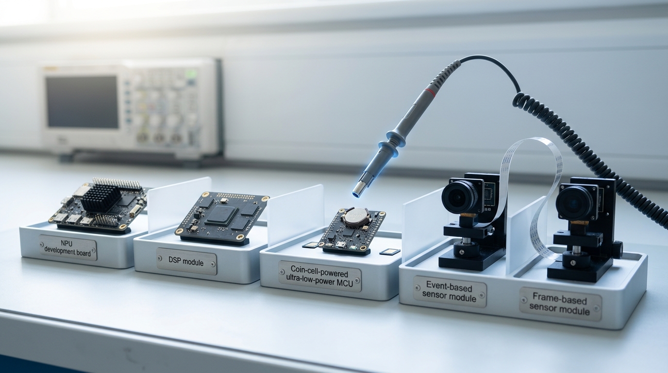
An edge AI system answers two separate design questions, and much confused comparison in this field comes from treating them as one. The first is where the arithmetic lives: does the multiply-accumulate work happen on silicon fixed at design time into a small, regular array, on a programmable digital signal processor built for continuous streaming math, or on the general-purpose CPU of an ultra-low-power microcontroller that spends nearly all its life asleep? The second is what the system is allowed to see: does a sensor hand the processor a complete rectangular frame at a fixed clock rate, with a companion processor stacked into the same package to discard most of that frame before it leaves the chip, or does each pixel report for itself, asynchronously, only when the light on it actually changes?
These two axes are independent. A frame sensor can feed a dedicated NPU, an event sensor can feed a general-purpose DSP, and an always-on microcontroller can be woken by either. This article works through three answers to the compute question and two to the sensing question, then asks what a reader should do with five options that do not reduce to one ranking. Two ground rules apply throughout. A vendor’s own generational or competitive comparison is evidence about that vendor’s part and does not automatically transfer to a different company’s silicon, node, or year. And where the engineers who build this hardware genuinely disagree about which approach wins for a given workload, the honest response is to describe the disagreement, not adjudicate it from outside.
The compute axis: three answers to where the arithmetic lives
The dedicated NPU or accelerator answer
A dedicated neural processing unit answers the scheduling question by refusing to leave it open. The multiply-accumulate array’s connectivity and reuse pattern are fixed once, in silicon, so the chip carries almost no instruction-fetch or branch-prediction logic — nearly its entire area and power budget goes to arithmetic and the small on-chip memory feeding it. Eyeriss, an academic accelerator whose “row-stationary” dataflow strategy influenced how commercial edge NPUs are built, demonstrates the argument cleanly: its 168 processing elements maximise local data reuse specifically to minimise the far more expensive movement of data to and from off-chip memory, and its designers report the chip running AlexNet at 35 frames per second on 278 milliwatts, about ten times the energy efficiency of a mobile GPU on the same task [5]. That is the accelerator’s core promise: an order-of-magnitude efficiency gain on the operations it was built for, in exchange for doing almost nothing else well.
Commercial microNPUs make the same trade at smaller scale. Arm markets its Ethos-U55 as “the world’s first microNPU,” paired with a Cortex-M-class CPU rather than deployed alone, and states the pairing delivers “a 480 times uplift in ML performance over existing Cortex-M based systems” while occupying roughly 0.1 square millimetres and cutting energy by up to 90% versus running the same workload on the CPU alone [11]. Those are Arm’s own disclosed figures for its own part — a vendor’s claim about its own comparison, not a portable constant. What the claim does establish structurally is the shape of the trade: an NPU this small only makes sense bolted onto a general-purpose core that handles everything the fixed array cannot, which is most of what an embedded application needs besides the neural network itself.
The DSP answer
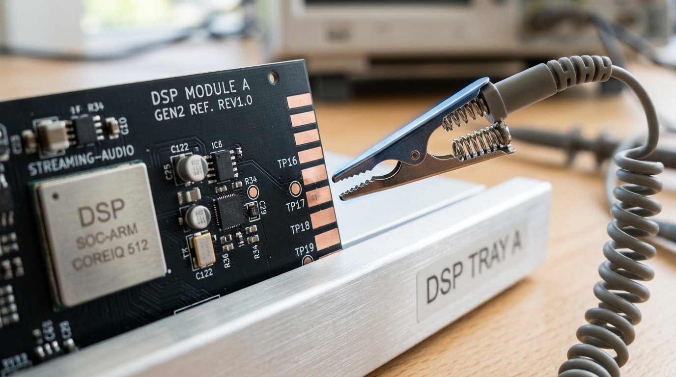
A digital signal processor keeps more of the general-purpose core than an NPU does, while still narrowing its instruction set toward the vector and multiply-accumulate operations that dominate both classical signal processing and neural inference. Where an NPU’s array has no meaningful instruction stream, a DSP is still a programmable processor executing compiler-generated code; the efficiency gain comes from a denser instruction set and wide SIMD math units rather than from removing scheduling logic altogether. Cadence positions its Tensilica HiFi and Vision DSP lines on exactly this middle ground, describing new cores built on the Xtensa LX8 platform that deliver “up to 3X improvement for certain AI workloads” on the vision side and “up to 2X” imaging and AI performance from added 8-bit operations on the audio side, while continuing to run the classical codec and filtering workloads DSPs have always handled [17]. The same announcement pairs these DSPs with a separate NPU product line through a shared software stack — a tacit admission that the DSP’s generality has limits for dense matrix work, and that many designs will use both rather than choosing one [17].
The DSP’s genuine advantage is not raw efficiency on a matrix multiply — a fixed array usually wins that specific contest — but continuity: the same core that classifies a keyword or gesture also runs the always-on audio front end, the sensor-fusion filter, and the wake-word detector without a second toolchain, because all of that was already a DSP’s job before neural inference existed. A fixed accelerator array cannot offer that continuity, which is why DSPs remain common where the neural workload is one job among several rather than the only job.
The always-on ultra-low-power microcontroller answer
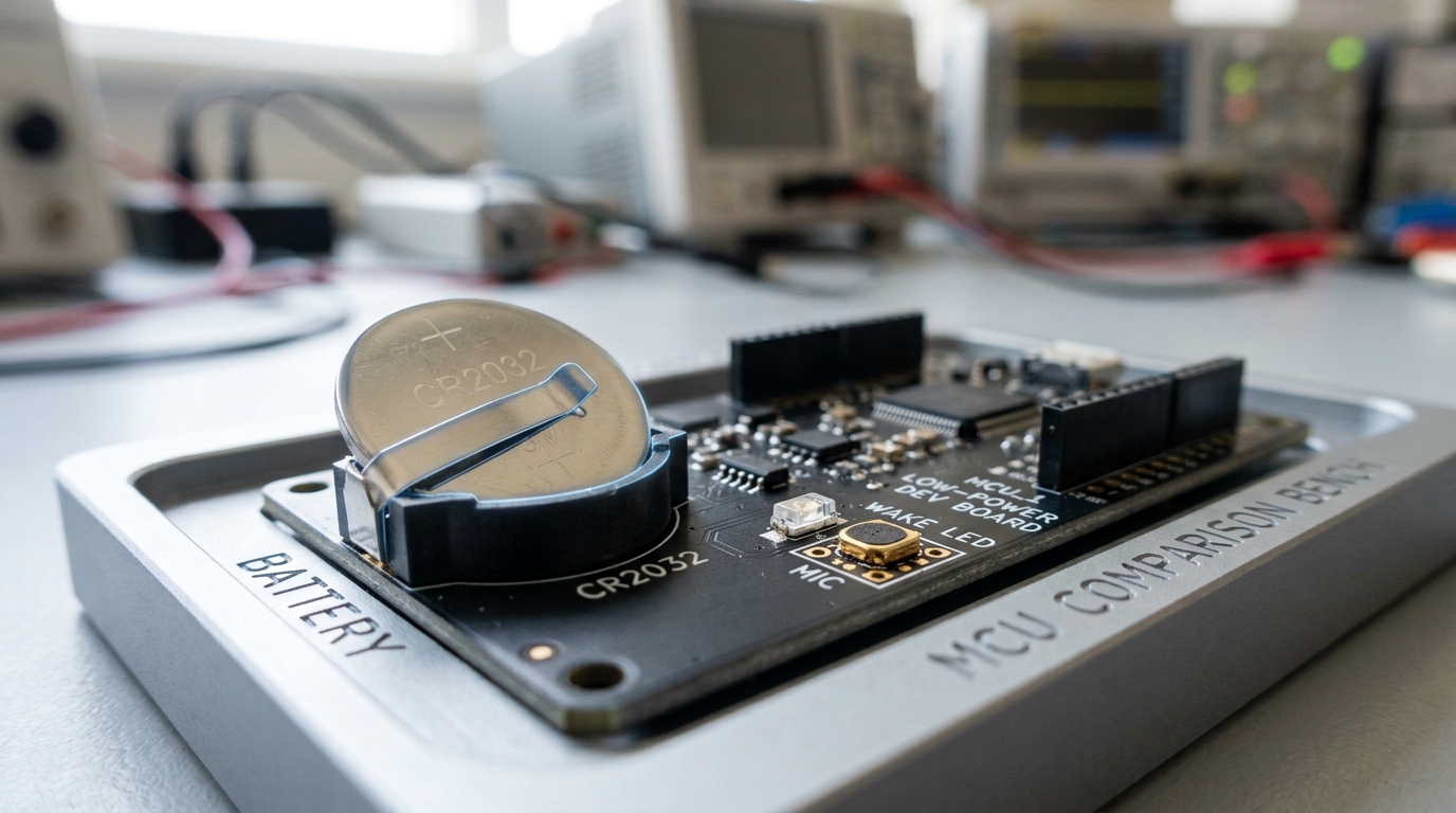
The third answer removes dedicated neural hardware altogether and asks how much inference a general-purpose microcontroller CPU can do on its own, at a power budget low enough to run continuously rather than only when triggered. This is a software problem as much as a hardware one: CMSIS-NN, Arm’s own library of neural network kernels tuned for Cortex-M CPUs, reports a “4.6X improvement in runtime/throughput and 4.9X improvement in energy efficiency” purely from better use of the SIMD and saturating-arithmetic instructions already present in the CPU, with no new silicon at all [7]. Google’s TensorFlow Lite Micro pushes the same idea into a full inference framework, built to run within, in its authors’ words, “a few kilobytes of memory” on exactly this class of processor [8].
MCUNet goes further and treats the neural architecture and the inference engine as one co-designed system: its authors report that jointly designing the search space (TinyNAS) with the memory scheduler (TinyEngine) reduces memory use by 4.8 times and speeds inference by 1.7 to 3.3 times compared with running the same class of model through TensorFlow Lite Micro or CMSIS-NN unmodified, and that the resulting system is “the first to achieve >70% ImageNet top-1 accuracy on an off-the-shelf commercial microcontroller,” using 3.5 times less SRAM and 5.7 times less flash than a quantised MobileNetV2 or ResNet-18 at comparable accuracy [6]. An always-on MCU is therefore not simply a weak accelerator running a shrunk model badly; software and search-space co-design can move the achievable accuracy-per-byte of memory substantially, independent of any change in silicon.
Silicon-level work pushes the same category toward genuinely continuous operation rather than periodic wake-and-sleep. Di Mauro and colleagues describe a 22-nanometre IoT chip running a binary neural network continuously at 674 microwatts and 4 giga-operations per second, and show that dropping supply voltage to 0.5 volts costs no accuracy at all on a CIFAR-10 classifier, improving energy efficiency by 2.2 times, while a more aggressive 0.42-volt point keeps over 99% of nominal accuracy despite an SRAM bit error rate near one in a thousand, tolerated by error-resilient design rather than avoided [14]. The point is architectural: “always-on” here can mean the inference itself runs continuously at the edge of correct operation, rather than a low-power core merely listening for a trigger to wake a bigger, hungrier processor.
An always-on system’s design target is not peak throughput but the average power drawn between the (usually rare) events that matter, which can be written as a simple duty-cycle model:
where
The sensing axis: two answers to what the system is allowed to see
Frame-based sensing with on-chip preprocessing
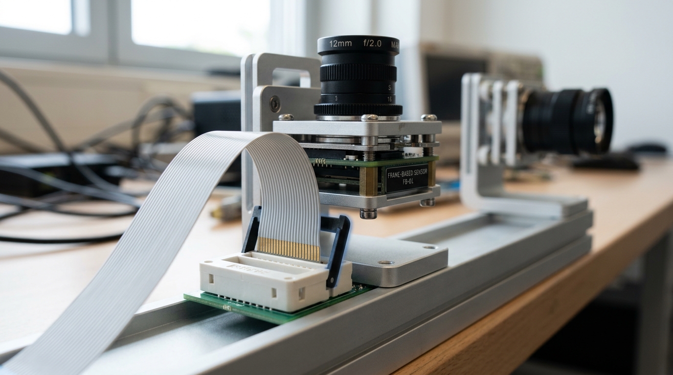
The conventional answer keeps the sensor’s operating principle unchanged — every pixel is read out together, on a fixed clock, into a complete rectangular frame — and moves the processing as close to the pixel array as physically possible instead. Sony’s IMX500 is the clearest commercial instance: a stacked device with a pixel die bonded directly to a logic die carrying, in the company’s own description, a “Sony-developed DSP and memory for the AI models,” so that capture and a full inference pass happen inside one package before anything leaves it. Sony states the sensor completes capture and inference using a MobileNet V1-class model in about 3.1 milliseconds, and that in a metadata-output mode the pixel data never has to leave the chip at all [12]. An independent matched-condition benchmark places the IMX500 alongside microcontroller-class and multi-core accelerator platforms and reports it “achieving the highest utilization (86.2 MAC/cycle) and the lowest energy-delay product” of the three on a shared segmentation workload [15] — consistent with the general logic that data movement, not arithmetic, is usually the dominant cost, so eliminating the trip off-chip before a full frame is even assembled is where a stacked sensor’s efficiency comes from.
This approach keeps everything else about frame-based imaging intact: the same fixed frame rate, the same complete readout regardless of how much of the scene changed, and the same downstream ecosystem of established computer-vision models and tools built around whole images. Its efficiency gain is architectural placement — moving the compute next to the data — rather than a change in what data is captured in the first place.
Event-based, neuromorphic-style sensing
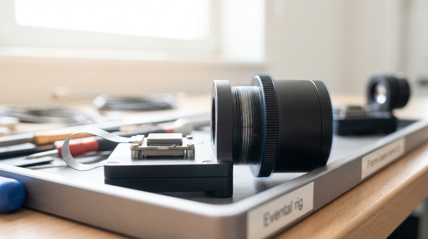
The second answer changes the sensing principle itself. In an event-based, or “dynamic vision,” sensor, each pixel operates independently and asynchronously, reporting a signed event the instant its local log-intensity crosses a threshold, rather than waiting for a shared frame clock. The foundational silicon demonstration, Lichtsteiner, Posch and Delbruck’s 2008 dynamic vision sensor, reported 120 decibels of dynamic range and 15-microsecond latency from a 128-by-128 pixel array using this asynchronous, per-pixel comparator design [1]. A later review by Posch and colleagues frames the motivation directly: bioinspired, event-based vision systems have “the potential to outperform conventional, frame-based vision systems… in terms of redundancy suppression and data compression, dynamic range, temporal resolution, and power efficiency” precisely because they discard the assumption that a full array must be re-sampled on every clock tick [2]. The field’s most-cited survey summarises the resulting characteristics as “high temporal resolution (in the order of microseconds),” “very high dynamic range (140 dB vs. 60 dB)” relative to standard cameras, and “low power consumption,” arising from the same asynchronous, brightness-change-triggered principle [3].
Commercial event sensors have reached production stacked-silicon form. The Sony-Prophesee IMX636 reports pixel latency under 100 microseconds at 1,000 lux, standby power of 5 milliwatts against a maximum of 205 milliwatts, and a peak event rate above one billion events per second across its 1,280-by-720 array [13]. Because a pixel only ever transmits when it individually crosses its change threshold, the sensor’s data rate scales with how much of the scene is actually changing, not with the pixel count or a fixed frame clock — the opposite dependency from a frame sensor’s fixed-rate readout:
where
Where the axes meet, and where they don’t have to
The two axes are formally independent, but not independent in practice, because each sensing principle produces data whose shape favours a different compute answer. A frame sensor’s fixed-size, fixed-rate array of pixels is naturally matched to a fixed spatial array of multiply-accumulate cells: a convolution slides over a rectangle, and an NPU or DSP’s SIMD lanes are built to process rectangles. An event sensor’s sparse, irregular, asynchronous stream of individually timestamped pixel addresses is not shaped like a rectangle at all, and most of the deep-learning toolchain — including the frameworks discussed above — was built assuming it would be. A common accommodation converts a short time window of events back into a frame-like tensor before handing it to a conventional NPU or DSP pipeline, recovering compatibility but giving back some of the sparsity that made the event sensor attractive. The more architecturally faithful match is a processor that is itself asynchronous and event-driven rather than clocked, of which Intel’s Loihi is the clearest research instance: a 60-square-millimetre, 14-nanometre spiking-neuroscience chip whose authors report that a spiking implementation of the Locally Competitive Algorithm solves LASSO optimisation problems with “over three orders of magnitude superior energy-delay-product” compared with the same problem on a conventional CPU [4]. No mainstream commercial edge product ships this compute model at volume today; it remains the sensing axis’s natural but still largely research-stage compute counterpart, so this article’s compute-axis comparison is confined to the three approaches that do ship in production designs.
The boundary blurs from the other direction too: Sony’s own description of the IMX500’s logic die names its on-chip processor a “DSP” [12] — meaning the sensing-axis “on-chip preprocessing” answer is, internally, one instance of the compute-axis DSP answer, just packaged inside the sensor rather than beside it on a separate board. Frame-based and event-based are less two different downstream compute problems than two different places to draw the boundary of what counts as “the sensor” versus “the processor.”
Why a single number cannot rank these five components
It is tempting to reduce all five options to one figure of merit — operations per second, or operations per watt — and the matched-condition study cited above is the clearest evidence against doing so. Capogrosso and colleagues benchmarked the same 336-million-multiply-accumulate segmentation workload, under the same methodology, across a multi-core RISC-V accelerator (GAP9), a Cortex-M55-with-NPU microcontroller (STM32N6), and an in-sensor processor (Sony IMX500), and found three different winners on three different axes: the in-sensor processor had the highest per-cycle utilisation and lowest energy-delay product, the microcontroller-class accelerator had the best energy efficiency within its power budget, and the NPU-equipped microcontroller had the lowest raw latency “at a significantly higher energy cost” [15]. That is not an unresolved measurement problem the field has failed to fix; it is what three genuinely different architectural bets look like when compared honestly on one workload, and it directly contradicts any single ranking a less careful comparison might offer.
The broader accelerator landscape makes the same point at larger scale. Reuther and colleagues’ recurring survey of AI and ML accelerators compiles disclosed performance and power figures across commercial parts specifically because no single vendor-neutral benchmark yet covers the field consistently, and it explicitly tracks neuromorphic, photonic, and memristor-based accelerators as separate emerging categories because their characteristics do not collapse onto the same axes as conventional silicon [16]. MLCommons’ response for the smallest end of the market is MLPerf Tiny, a benchmark built to standardise measurement conditions across microcontroller-class, DSP-class, and accelerator-class edge hardware so at least the workload and methodology are held fixed even when the silicon is not [9]. At the sensing layer, IEEE 2700 exists for the same reason one level down: a standard vocabulary and set of required conditions for reporting sensor performance parameters, so a dynamic-range or latency figure from one vendor’s datasheet means the same thing as the equivalent figure from another’s [10]. All three responses point the same direction — toward matched, disclosed measurement conditions — because none of these fields currently has a single number that means the same thing across architectures.
Where the real disagreements are
Three disagreements in this space are genuine and unresolved among the people who build this hardware, not manufactured for the sake of balance.
The first is whether the DSP remains a durable third category on the compute axis or is being absorbed at both ends — its signal-processing workloads migrating to fixed accelerator blocks, its general-purpose flexibility ceded to the CPU. The case for absorption is visible in Cadence’s own product strategy, which now pairs its DSP line with a separate NPU family under one software stack rather than asking the DSP alone to cover both jobs [17]. The case against is that the DSP’s core advantage — one toolchain, one core, covering classical filtering, sensor fusion, and neural inference without context-switching between separate chips — has no real substitute when a product’s neural workload is small relative to its non-neural signal-processing load, which describes much always-listening audio and sensor-fusion hardware. Nothing in the public record settles which force wins, and this article does not either.
The second is whether the efficiency case for event-based sensing is a property of the sensor or a property of the scene. The architectural case is strong and well evidenced: Posch and colleagues’ and Gallego and colleagues’ independent reviews both attribute large power and bandwidth advantages directly to the asynchronous, threshold-triggered pixel design [2] [3]. The scene-dependence argument, developed analytically above from that same operating principle, is equally well grounded: a sensor whose data rate is proportional to the number of pixels currently changing state offers its largest advantage exactly when little is happening, and that advantage shrinks in the textured, high-motion conditions many vision applications actually target. Both claims are true simultaneously; they describe different operating regimes of the same device, and a fair comparison has to specify which regime it measured in.
The third is whether always-on microcontroller-class inference is fundamentally a wake-up filter for a more capable downstream accelerator, or an increasingly capable endpoint in its own right. The wake-up-filter view is supported by the duty-cycle model above: for the rare-trigger workloads this category is classically used for,
Privacy, control, and field reliability
Two of the five options carry a privacy property the others do not offer by default: an in-sensor processor that outputs only inference metadata, as Sony describes for the IMX500’s metadata-output mode, never transmits the image itself off the chip [12], and an event sensor’s sparse, brightness-change-only output structurally withholds most of the scene’s static content — a still background produces almost no events regardless of what it depicts. Both properties are architectural, not policy: a system built this way cannot leak a full frame it never assembled, a stronger guarantee than a software policy promising not to transmit one. That guarantee has a real limit worth stating plainly — a determined observer can often reconstruct a rough scene from a long enough sequence of sparse events or repeated metadata, so “privacy by architecture” narrows what a compromised or curious downstream system can extract; it does not eliminate the question.
Field reliability differs across the same options for reasons that follow from their own design targets. A duty-cycled, always-on microcontroller’s dominant failure mode over years of deployment is drift in its wake-trigger threshold as battery voltage sags and temperature swings, not silicon wear-out; the aggressive voltage scaling that gives the always-on binary-neural-network chip discussed above its efficiency also narrows its margin against that drift, which is why its designers built error-resilient memory and accuracy-preserving voltage floors into the chip rather than treating the nominal operating point as the only one that matters [14]. A dedicated NPU’s fixed dataflow has no equivalent adaptive margin — it either supports a given operator shape or it does not — trading field-reliability risk for a simpler, more predictable failure surface. An event sensor’s per-pixel independence means a single stuck or noisy pixel degrades gracefully as one bad address in a stream rather than corrupting a shared frame buffer, a reliability advantage that follows directly from the same architectural choice that gives it its bandwidth properties.
Reading rules for anyone evaluating an edge AI system
A short discipline follows from all of the above, regardless of which of the five options a given evaluation favours.
Ask which axis a claimed advantage actually belongs to. A power or latency number attributed to “the sensor” or “the chip” is frequently a property of the paired compute-and-sensing combination actually measured, not of either component alone.
Never carry a single-vendor comparison across companies, nodes, or years. Every dated efficiency or throughput figure in this article, including Arm’s own 480-times and 90%-reduction figures for Ethos-U55, describes that vendor’s progress against its own prior or competing hardware under conditions it chose, and none of them composes with a different vendor’s equivalent claim.
Ask what scene or workload regime a sensing claim was measured in. An event sensor’s efficiency advantage and a frame sensor’s predictability are both real, and both are conditional on how much of the scene is actually changing.
Treat matched-condition studies as more informative than any single headline number, even when — especially when — they report multiple winners rather than one, because a study reporting three winners on three axes is describing the actual shape of the tradeoff rather than collapsing it.
Predictions, with what would falsify them
These are forecasts, clearly separated from the sourced analysis above. Horizon: 16 August 2030.
One. In-sensor and near-sensor processing will keep gaining share for vision-specific edge products over discrete sensor-plus-NPU pairs, because the energy-delay-product advantage documented by matched-condition benchmarks like Capogrosso and colleagues’ follows from data-movement physics rather than a temporary process-node lead. Disconfirmed if discrete sensor-plus-accelerator pairs close the energy-delay-product gap to in-sensor processing on a matched published benchmark within the horizon.
Two. Event-based sensors will remain concentrated in applications with genuinely sparse, mostly-static scenes — industrial monitoring, low-duty-cycle triggers, high-speed sparse-motion tracking — rather than displacing frame-based sensing generally, because the scene-dependent data-rate argument above is a property of the sensing principle, not a solvable engineering gap. Disconfirmed if event-based sensors become the default choice for dense, continuously textured scenes such as general outdoor object detection at standard frame rates.
Three. Always-on microcontroller-class inference will keep expanding its capability at fixed memory and power faster than dedicated accelerators shrink their idle floor, following the trajectory MCUNet’s co-design results already show, which will blur rather than sharpen the boundary between “wake-up filter” and “endpoint.” Disconfirmed if published microcontroller-class accuracy-at-fixed-memory results plateau while dedicated-accelerator idle power continues falling at its current rate.
Four. Matched-condition, standardised benchmarking — in the mould of MLPerf Tiny and IEEE 2700 — will become the expected basis for edge AI hardware comparison, and single unconditioned throughput or efficiency numbers will draw more visible pushback in technical venues. Disconfirmed if single-number, unconditioned comparisons remain the dominant form of edge AI hardware marketing and reporting through the horizon with no comparable methodological pushback.
What to take away
Five components, two independent questions. Where the arithmetic lives has three real answers: fixed into a fast, narrow array; general but streamlined in a DSP; or run in software on a general-purpose microcontroller CPU tuned for a near-zero idle floor. What the system is allowed to see has two real answers: a complete frame, processed as close to the pixel array as the package allows, or a sparse, asynchronous stream of individual brightness changes. None of the five is a strictly dominant choice, and a matched-condition study that actually measures more than one of them side by side — the clearest evidence in this article — found three different winners on three different axes on a single shared workload.
The question worth asking of any edge AI hardware claim is not “which is better,” but “measured how, on what workload, in what scene, against which of that vendor’s own prior parts” — and a comparison that supplies a ranking without answering all four has quietly chosen them for you.