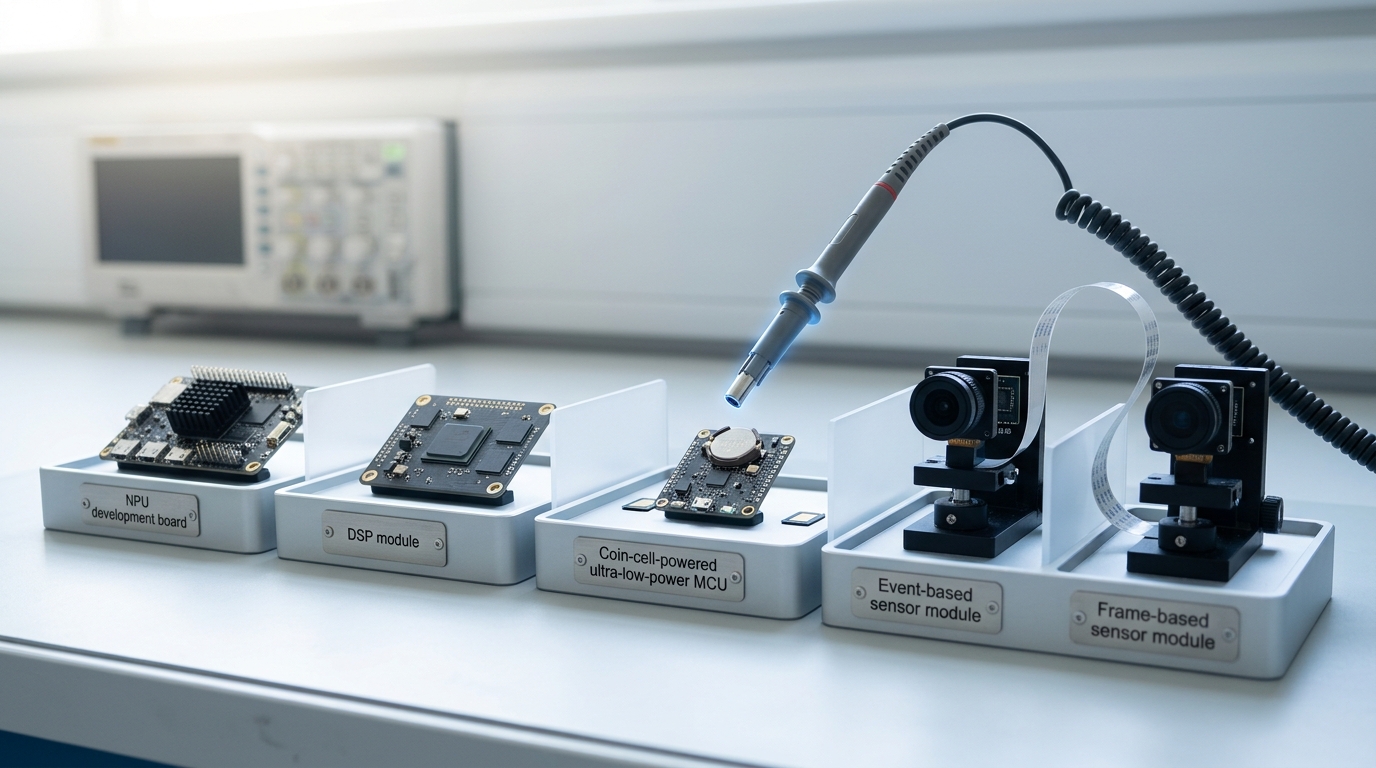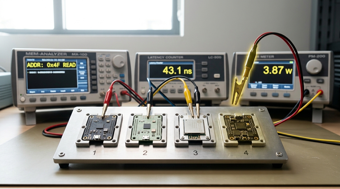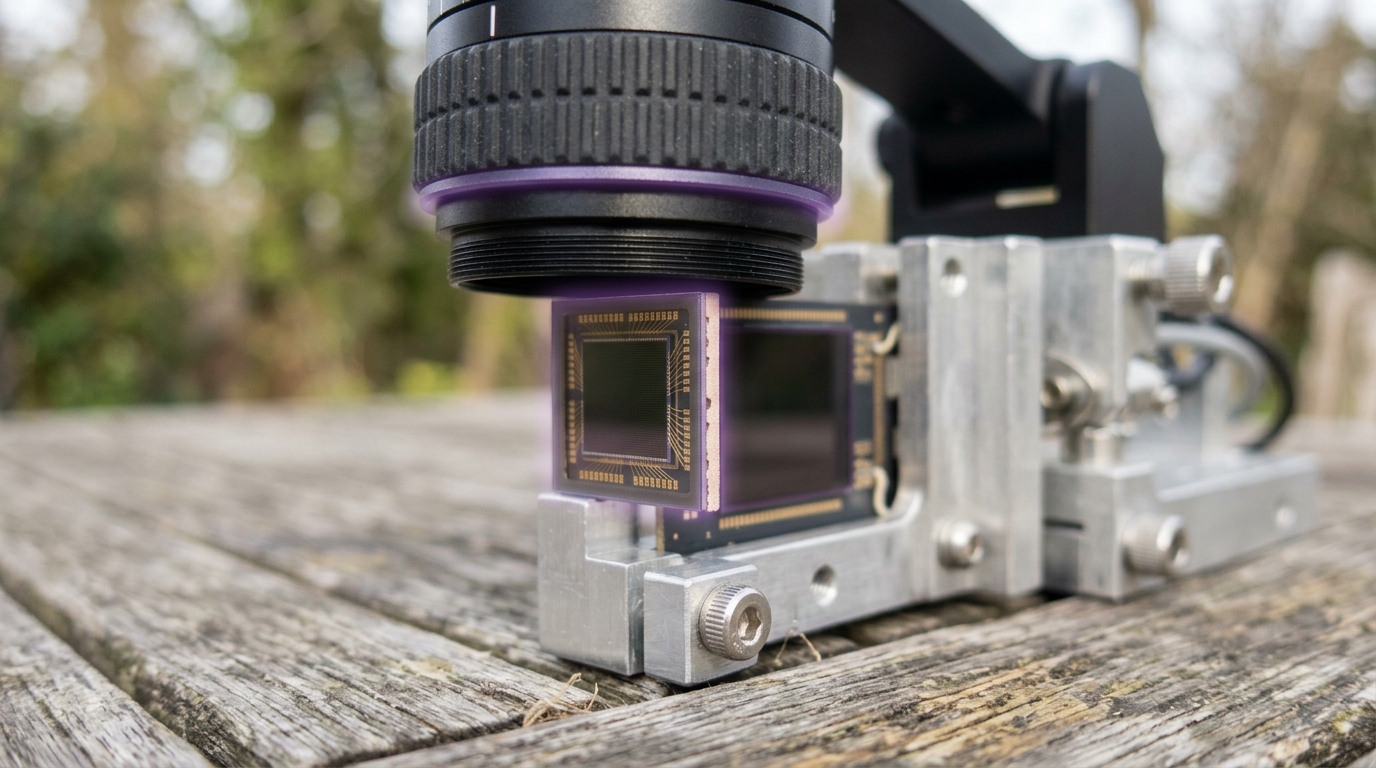
A signal has to survive four translations before a model ever sees it
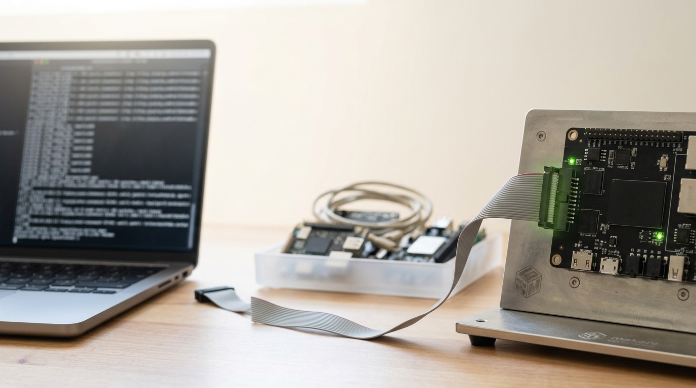
A doorbell camera notices someone at the door. A wearable notices a wrist rotating. A factory sensor notices a bearing starting to vibrate at a new frequency. In every one of these cases the thing being noticed is a continuous physical quantity — light, sound pressure, acceleration — and the thing that eventually acts on it is a digital neural network running on a chip that may have a power budget measured in single-digit milliwatts, or, for the part of the system that is always listening, in microwatts. Between the physical event and the model’s output sits a chain of hardware that gets almost no attention in discussions of “edge AI,” which tend to jump straight from “sensor” to “inference” as though the middle were a solved, boring wire.
It is neither solved nor boring, and it is not one translation but several, each with a name, a failure mode, and a body of device literature behind it. A physical signal has to be transduced into an electrical one; that electrical signal has to be conditioned and digitized by an analog front end; a decision has to be made, continuously and at near-zero power, about whether anything worth reporting has happened at all; and only when that decision is yes does a quantized neural network get to spend its power budget on an actual inference. This article works through those four stages in order, using an event camera — a sensor that only reports pixels that changed, rather than every pixel on a fixed clock — as the clearest illustration of how differently edge hardware treats data compared with the frame-and-datacenter assumptions most AI writing carries over by habit.
None of this is exotic. It is the ordinary, decades-deep discipline of analog and mixed-signal circuit design meeting a newer requirement: that the far end of the chain now runs a neural network instead of a fixed-function filter. The mechanisms are well characterized in device physics and circuits literature; what follows draws directly on that literature rather than on marketing description of any particular chip, and marks the difference explicitly wherever it matters.
The physical signal becomes a voltage, briefly, on purpose
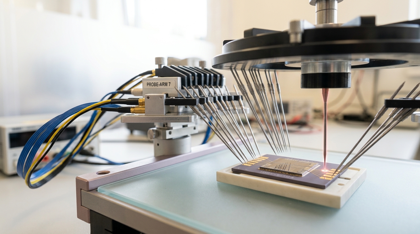
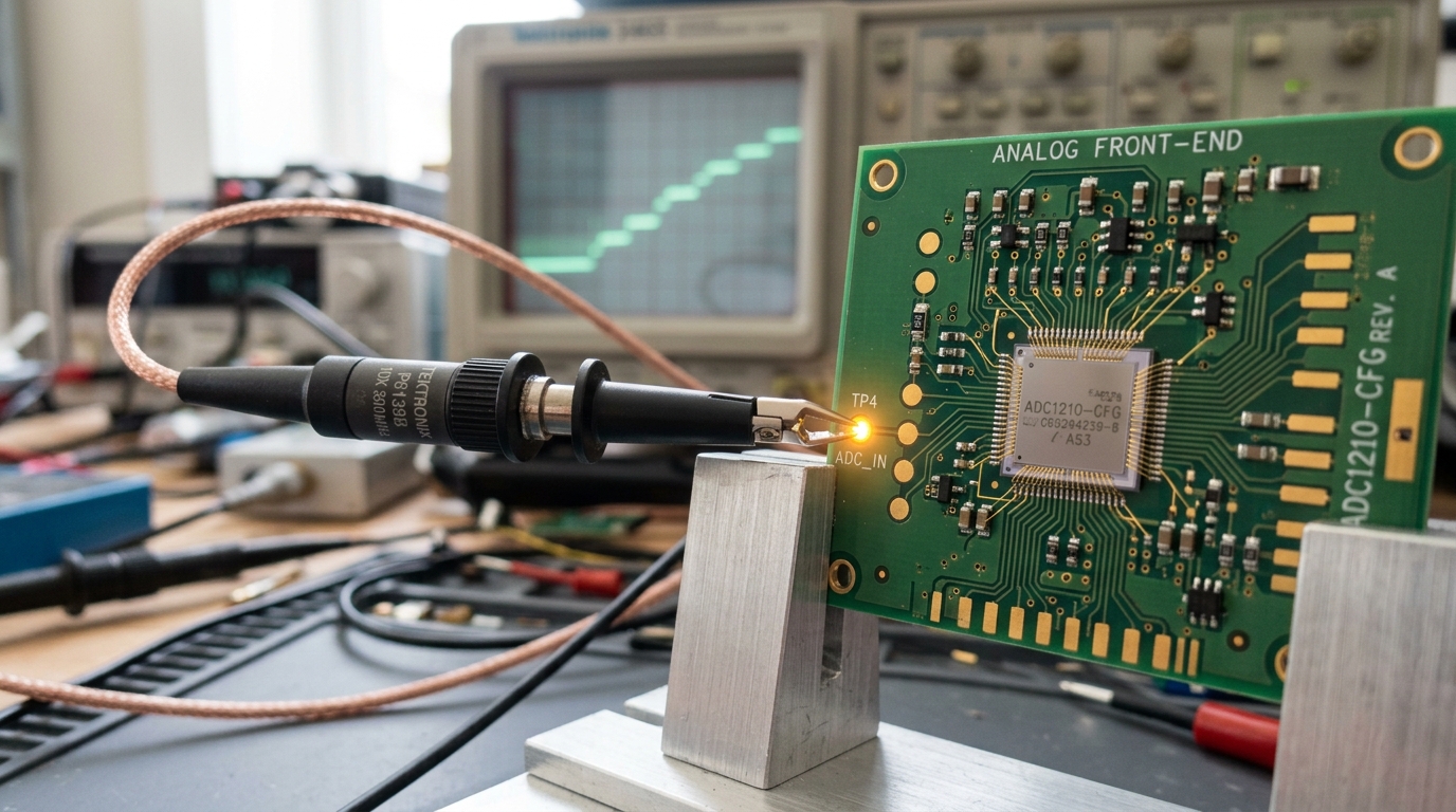
Nothing a digital system can use exists yet at the sensor. A MEMS accelerometer’s proof mass shifts a few nanometres and changes a capacitance by femtofarads; a photodiode’s current shifts by picoamps; a microphone’s diaphragm moves by less than the width of an atom for a quiet voice. None of that is a number a processor can read. The first job of the electronics is transduction — converting the physical quantity into a voltage or current — and the second job, done by what circuit designers call the analog front end (AFE), is to condition that tiny, noisy electrical signal enough that a data converter can turn it into a stable digital code.
This stage is where most of the difficulty in “sensing” actually lives, and it is a genuinely hard analog design problem rather than a solved commodity. Consider a capacitive MEMS accelerometer: the sense element’s output is a change in capacitance riding on a much larger fixed capacitance, and the amplifier that reads it is itself a source of the noise it is trying to measure below. A 2026 circuit study of a low-noise AFE for capacitive MEMS accelerometers used a fully differential chopper-stabilization technique specifically to push the amplifier’s own low-frequency 1/f noise out of the signal band, reporting a measured sensitivity of 342 millivolts per g, 1.1% nonlinearity, an 88 dB dynamic range, and a noise floor of 14 micro-g per root-hertz for a device aimed at handheld camera stabilization [10]. Every one of those numbers is a property of the front-end circuit, not of the mechanical sensor alone — the same MEMS element paired with a worse amplifier would report a worse noise floor.
Once the signal is a clean, conditioned voltage, it has to become a digital code, and that conversion is not free either. An analog-to-digital converter maps a continuous voltage onto one of
Why an event camera is not a slow-shutter camera
Conventional image sensors read every pixel, every frame, on a fixed clock, whether or not anything in the scene changed. For an edge system that is mostly looking at an unchanging world — a hallway, a parked car, a resting hand — that is a strange design: it spends the same bandwidth and the same energy on a static frame as on a frame full of motion, and it still has a bounded temporal resolution set by the frame rate no matter how fast the actual event was.
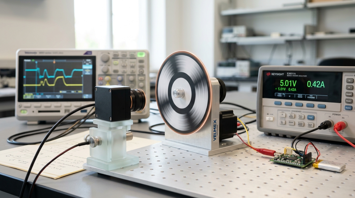
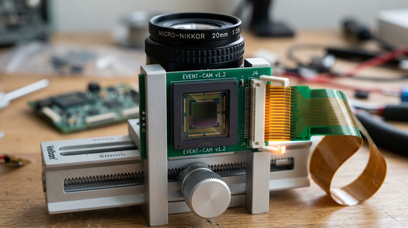
An event camera, more precisely a dynamic vision sensor (DVS), inverts that design at the pixel level. Each pixel contains its own small analog circuit — a photoreceptor, a differencing amplifier, and a pair of comparators — that continuously tracks the logarithm of local light intensity and fires an asynchronous digital event only when that log-intensity has moved by more than a threshold since the pixel’s last event. Formally, a pixel emits an event when
where
That last property is the one that matters most for edge deployment. A frame sensor pointed at an empty room outputs the same data volume as one pointed at a busy street; an event sensor pointed at the empty room outputs almost nothing, because almost nothing changed, and downstream logic can often stay idle. The sensor’s own analog bias currents — contrast threshold, bandwidth, and a refractory period that limits how fast a single pixel can re-fire — set the tradeoff between missing real changes and drowning in noise events, and getting that tradeoff right in the field, as illumination and temperature drift, is itself an active control problem: a 2021 paper from the sensor’s original research group proposes closed-loop feedback controllers that continuously adjust these bias currents from measured event rate and noise statistics, rather than leaving them fixed at a factory-calibrated value [3]. That is a fact about a specific published control scheme, not a claim about what any particular commercial event camera does out of the box.
It is worth separating fact from marketing claim on one more point. Because event streams are sparse and encode moving edges rather than dense, continuously refreshed pixel values, they are frequently described — by researchers and vendors alike — as inherently more privacy-preserving than continuous video. That description understates the actual state of the art: the same event-vision literature that documents the sensor’s sparsity also documents algorithms that reconstruct plausible full intensity video from an event stream alone, so sparsity by itself is not a privacy guarantee — what a system actually discloses depends on what is done with the stream downstream of the sensor, not on the sensor’s output format in isolation [2].
Most of the system is supposed to be asleep
An event-driven sensor already does some of the work of an always-on architecture by construction — it produces almost no output when nothing is happening — but the logic reading that sensor, and the neural network waiting to act on it, still need their own power discipline. The general pattern used across always-on edge systems is hierarchical: a very small, very low-power stage runs continuously, watching for a coarse trigger condition, while a much more capable but much hungrier stage — a full microcontroller, an embedded NPU, a radio — stays powered down or clock-gated until the small stage decides it is worth waking it.
The economics only work if the always-listening stage is extraordinarily cheap to run continuously, because “continuously” for a battery-powered device can mean years. A 2021 paper describes a spiking-neural-network classifier built specifically for this always-on role, using spike-driven clock- and power-gating so that circuit blocks are only active when a spike is actually present to process, reporting sub-microwatt static power for the always-on listening function [9]. The underlying technique is standard digital low-power design — clock gating stops a clock signal from toggling logic that has nothing to do, power gating disconnects supply rails from blocks that are fully idle — applied aggressively and asymmetrically: the rarely used, power-hungry path gets none of the optimization effort, because it runs rarely; the constantly-running trigger path gets almost all of it, because it runs constantly. The resulting system-average power is dominated by whichever stage is active for more time, which, by design, is nearly always the microwatt-class trigger rather than the milliwatt-class network.
This is also where the earlier two sections connect directly. An event-driven sensor is, in effect, its own wake trigger: because it only produces data when its threshold condition is crossed, a downstream system can treat “an event arrived” as the wake signal itself, rather than running a separate always-on classifier over a continuously sampled frame stream. Whether a given product actually wires it that way, or instead runs a small dedicated audio or motion trigger ahead of a frame- or event-based vision stage, is a design choice made per system, not a universal architecture — the literature describes multiple hierarchical patterns rather than one canonical one, and this article does not claim any single commercial device implements a specific combination unless cited.
What actually happens inside an embedded NPU
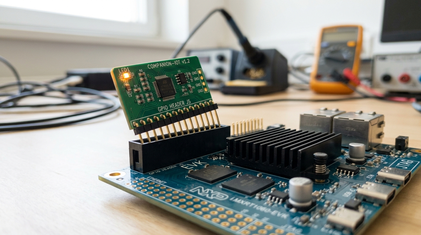
When the trigger does fire, the awakened stage has to run a neural network inside a power and latency budget that is orders of magnitude tighter than anything in a datacenter. Two levers do almost all of the work: shrinking the arithmetic, and building hardware whose data movement matches that shrunk arithmetic instead of fighting it.
The arithmetic-shrinking lever is quantization. A widely used scheme maps a real-valued weight or activation
with a scale
The data-movement lever is the accelerator’s dataflow — how weights, activations, and partial sums are staged in on-chip memory and reused across the array of multiply-accumulate units rather than re-fetched from memory for every operation. A widely cited 2017 survey of DNN accelerator design lays out this taxonomy explicitly: architectures differ by what they hold stationary in local storage — weights, outputs, or a mix — because moving a value into and out of memory is itself an energy cost, on top of whatever the arithmetic costs, and a design that minimizes redundant data movement can win even when it is not the fastest at raw multiply-accumulate throughput [4]. Two concrete embedded results illustrate what this buys in practice, reported by their own authors as measured results rather than theoretical peaks. A software kernel library for ultra-low-power parallel RISC-V clusters, built around exactly this kind of quantized, data-movement-aware execution, reports up to 15.5 8-bit multiply-accumulate operations per cycle on that hardware [6]. And Arm’s Ethos-U55, described by Arm as the first in a class of “microNPU” accelerators meant to sit beside a small Cortex-M microcontroller core, is stated by Arm to occupy roughly 0.1 square millimetres of silicon while delivering, in Arm’s own published figures, up to a 480-fold uplift in machine-learning performance compared with running the same workload on the Cortex-M core alone — a vendor performance claim, not an independently reproduced third-party benchmark, and one that like all such multipliers depends heavily on which baseline workload was chosen for the comparison [7].
The part nobody benchmarks: field reliability
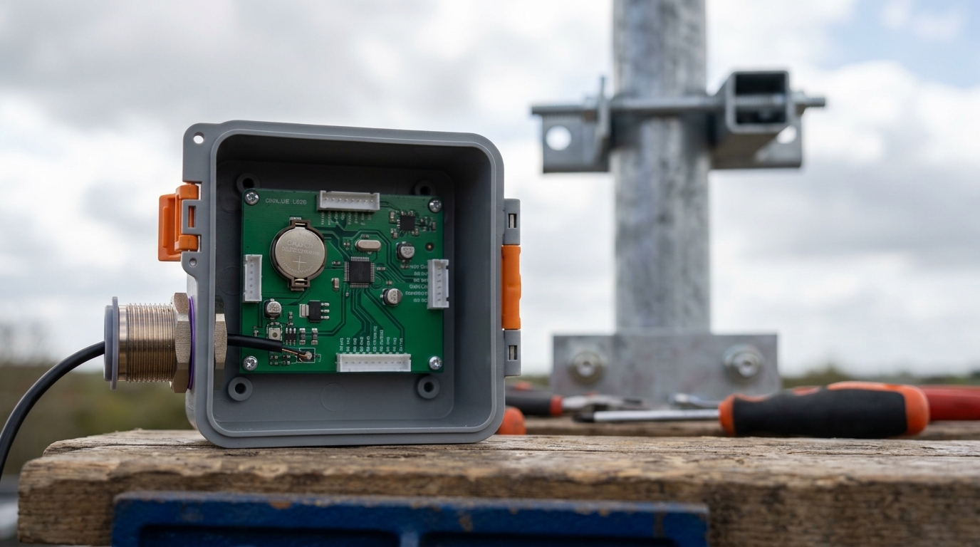
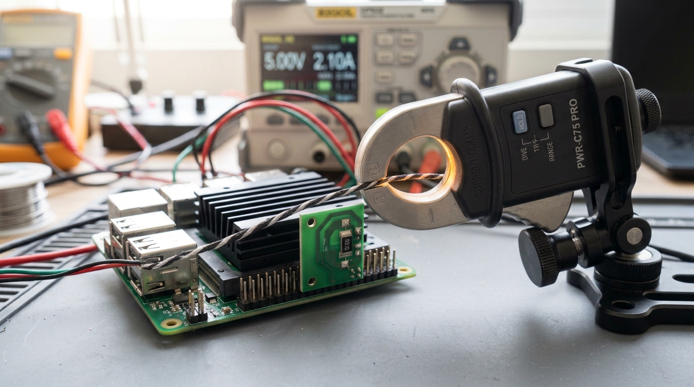
A device characterized once on a bench at room temperature is not the device that has to keep working for years inside a doorbell, a hearing aid, or an industrial gearbox, and this gap is where a surprising amount of edge-AI hardware literature actually concentrates its effort.
On the analog side, drift is the enemy: the same offset and 1/f noise that a chopper-stabilized amplifier suppresses at calibration time will re-emerge as temperature, supply voltage, and device age shift, which is exactly why techniques like chopper stabilization and oversampled noise-shaping are described in the circuit literature as continuous, running mitigations rather than one-time calibration steps [10] [11]. It is also why a shared, standardized vocabulary for describing converter error — the offset error, gain error, and linearity terms defined by IEEE 1241 — matters operationally and not just administratively: a system integrator choosing between converters, or debugging a field failure, needs those terms to mean the same thing across every datasheet they read [12]. On the sensing side, the same point applies to event cameras: the bias currents that set contrast threshold and noise floor are not “set once” but need active, measured feedback control as conditions drift in the field, which is the entire premise of the closed-loop bias controllers described earlier [3].
On the compute side, a 2024 study of Arm’s Ethos-U55 accelerator looked specifically at reliability under transient hardware faults — soft errors caused by phenomena like cosmic-ray-induced particle strikes flipping a bit in memory or logic — and evaluated the chip against the ASIL-D standard used for safety-critical automotive and medical systems. Using register-transfer-level fault injection, the authors found that all four configurations of the NPU they tested fell short of the resiliency that standard requires, and rather than recommending the traditional (and expensive, roughly 100% area overhead) fix of full dual-core lockstepping, they proposed selectively hardening only the components most sensitive to faults, reaching ASIL-D-level resiliency in their analysis at closer to 38% area overhead [8]. That is a measured, independent finding about the gap between a commercial embedded accelerator as shipped and what safety-critical deployment actually demands — the kind of result that a performance datasheet alone would never surface, and a useful corrective to treating “it runs the network fast” as equivalent to “it is ready for the field.”
What this buys, and what it costs
Put the four stages back together and the shape of an edge AI system becomes a shape rather than a black box: a transducer and an analog front end that spend real circuit-design effort converting a physical quantity into a trustworthy digital code; a sensing architecture — event-driven or otherwise — that decides how much of that code stream is worth keeping at all; a hierarchy of wake logic that keeps almost the entire power budget switched off almost all of the time; and, only at the end, a quantized neural network running on hardware built specifically to avoid moving data any further than it has to.
Every stage exists because the one obvious alternative — do it the datacenter way, sample everything continuously at full precision, run a full-precision network on all of it, and let a battery or a thermal budget absorb the cost — does not fit inside a coin-cell or a bearing housing. Each translation in the chain is a deliberate, named engineering decision with a measured cost, documented in circuits and systems literature that rarely gets cited in higher-level discussions of “AI at the edge.” Reading a specification for any one of these stages in isolation — a converter’s resolution, a sensor’s dynamic range, an accelerator’s peak throughput — without asking what analog front end fed it, what woke it, and what field conditions it was actually characterized under, is the surest way to be surprised by a real deployment. The chain is only as trustworthy as its weakest translation, and that translation is very often the one nobody thought to benchmark.