Why this piece separates five different kinds of claim
Every forecast about edge AI electronics mixes at least five kinds of statement, and most of the bad ones mix them silently. A fact is something measured and reported, such as a chip’s tera-operations-per-second-per-watt figure in a peer-reviewed paper. A vendor assertion is a manufacturer’s own claim about its own product, true or not, stated by a party with an interest in the answer. Analysis is a chain of reasoning from facts to an implication. A scenario is one internally consistent way the future could unfold, stated conditionally. A prediction is a scenario the author is willing to be wrong about in public, on a stated date, against a stated observation.
This article keeps those five apart deliberately, because the edge AI electronics literature is unusually prone to collapsing them. A market-research slide that quotes a chipmaker’s peak TOPS figure, silently drops the word “peak,” and presents it beside a different vendor’s sustained figure has already committed the sin this piece exists to avoid. The scope, set by the assignment behind this piece, is four dated questions: how on-device model capability trades against a roughly fixed power budget; whether event-camera and neuromorphic sensing become mainstream rather than niche; whether privacy-preserving on-device inference becomes a regulatory requirement rather than a design preference; and what could force a discontinuity in any of the above. The horizon for every prediction below is 2035.
The compute-per-watt ceiling and what sits inside it
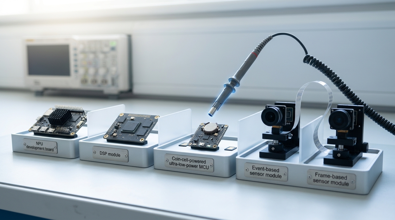
Start with the physical constraint that makes “edge” a different problem from “datacenter”: the power envelope is fixed by the device, not by the workload. A coin-cell sensor node has a milliwatt-scale budget set by battery chemistry and a multi-year service-life target. A phone’s neural accelerator has a budget set by a thermal design point and a battery a user expects to last a day. A satellite payload has a budget set by a solar array and a radiator. In every case, unlike a datacenter rack where more power can, within limits, be provisioned, the ceiling on an edge device is close to fixed by the product category itself, and getting more capability under that fixed ceiling can only come from doing more with each watt.
That structural fact can be written compactly. If
This is not a scaling law in the sense of a fitted curve; it is closer to an accounting identity, and its value is in what it rules out. Because
None of this is visible from a peak-TOPS spec sheet, which is precisely why an independent, standardized benchmark matters for edge parts in a way it matters less for datacenter accelerators, where a workload can usually be resized to fit whatever hardware is available. MLPerf Tiny, built by a coalition of more than fifty organizations, measures accuracy, latency, and energy together on four small, representative tasks — keyword spotting, visual wake words, image classification on tens of kilobytes of model, and anomaly detection — specifically because a part’s peak efficiency number and its efficiency on a real, sub-milliwatt-class workload can diverge substantially once memory movement, quantization loss, and duty-cycling are accounted for [2]. Any claim about on-device capability growth that does not distinguish peak
Event cameras and neuromorphic sensing: real numbers, narrow footholds so far
Event cameras are not a speculative sensor category; they are a shipping one, with a specific and well-documented departure from conventional imaging. Instead of reading out a full frame at a fixed rate, each pixel independently reports a brightness-change event, asynchronously, the moment it crosses a threshold. Gallego and colleagues’ survey of the field, itself a foundational document for anyone entering it, catalogues the resulting properties as measured rather than promised: microsecond-scale temporal resolution, roughly 140 decibels of dynamic range against roughly 60–70 decibels for a good conventional sensor, and power draw that scales with scene activity rather than with frame rate, because a static scene simply produces no events to report [1]. Those are facts about the sensing principle, established across a large body of peer-reviewed work, not a single vendor’s characterization.
The commercial foothold is real but narrow. Sony’s IMX636 and IMX637, developed jointly with Prophesee and announced in September 2021, are stacked event-based vision sensors using Sony’s copper-to-copper hybrid-bonding process, with the IMX636 reaching what Sony describes as the industry’s smallest pixel pitch for a stacked event sensor at 4.86 micrometres, at roughly 0.92 and 0.33 megapixels of spatial resolution respectively [7]. That is a vendor’s own characterization of its own part, and it should be read as one — a manufacturer describing a real, shipping product, not an independent benchmark of it. The stated target applications in that same release are telling: predictive maintenance and industrial vibration or spark detection, not general-purpose scene understanding. That is analysis, not the vendor’s own framing, but it follows directly from where the part is actually being designed in: applications where the asynchronous, sparse output is a near-perfect match for the task, rather than applications where a mainstream camera pipeline is simply being replaced.
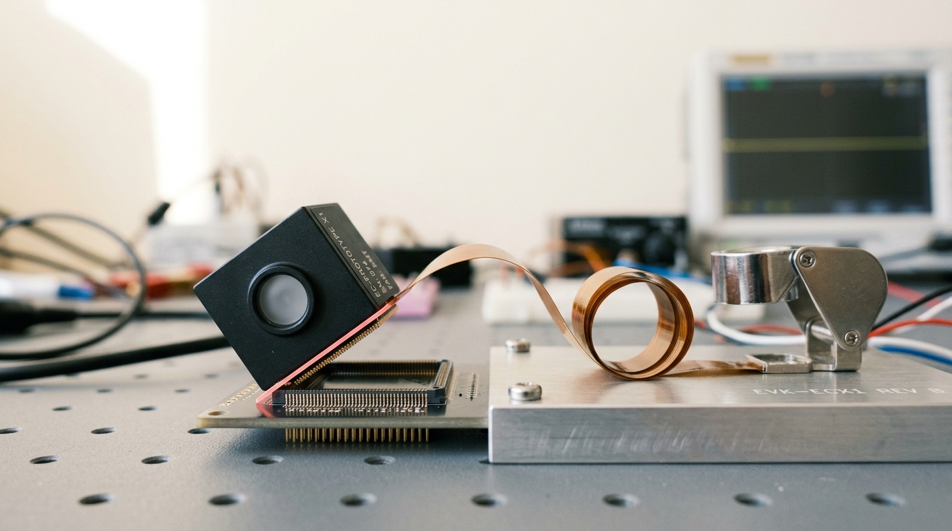
A closely related but architecturally distinct sensing bet is neuromorphic, spike-based computation downstream of the sensor. Intel’s Loihi research chips are the most extensively documented example in the peer-reviewed literature. Davies and colleagues’ survey of results obtained across the Loihi programme reaches a carefully qualified conclusion that is more useful, precisely because it is not a blanket endorsement: conventional feedforward deep networks show little or no benefit from running on spiking neuromorphic hardware, while networks that genuinely exploit recurrence, precise spike-timing relationships, synaptic plasticity, and sparsity achieve orders-of-magnitude lower latency and energy on some tasks compared with conventional approaches [5]. That is the honest state of the evidence: neuromorphic compute is not a general accelerator for today’s deep learning workloads, it is a strong fit for a specific and comparatively narrow class of temporally sparse, event-driven problems — of which event-camera output is one of the best-matched examples that exists.
Put the sensing and compute halves together and a scenario, not a fact, emerges: event cameras and neuromorphic processing are complementary technologies whose combined mainstream adoption depends on finding applications where both halves’ narrow strengths overlap with a market large enough to fund further silicon generations — industrial monitoring, some classes of automotive perception, and low-power always-on wake sensing are the current candidates. Whether that overlap is large enough to pull the pairing out of a niche by 2035 is exactly the kind of question this piece returns to in its predictions, rather than answering here as though it were already settled.
Privacy by architecture: what regulation actually requires today, and what it does not
It is tempting to state, as a fact, that regulation now requires privacy-preserving on-device AI. That statement is not yet true, and getting the distinction right matters for anyone planning silicon or product roadmaps around it. The EU’s Artificial Intelligence Act, formally Regulation (EU) 2024/1689, was published in the Official Journal on 12 July 2024, entered into force the following month, and applies in stages through August 2027 [3]. It is a risk-based regulation: it classifies AI systems by risk tier and imposes obligations — data governance, technical documentation, transparency, human oversight, and conformity assessment for high-risk systems — that scale with that tier. It does not, as a matter of the text itself, mandate that inference happen on-device, and it is analysis, not a citation to the Act, to say that its data-governance and minimization-adjacent obligations create a strong structural incentive toward architectures that keep raw personal data from leaving a device in the first place, because doing so sidesteps entire categories of the obligations that attach to processing and transferring that data elsewhere.
The same distinction holds for the other major reference point in this space, the NIST Privacy Framework, first published in 2020 as a voluntary risk-management tool rather than a binding rule. It organizes privacy practice around identifying, assessing, and managing privacy risk across a system’s lifecycle, with data minimization — collecting and processing no more than a stated purpose requires — as a recurring theme across its guidance [6]. Again: a voluntary framework that rewards minimization is not the same claim as a law that mandates on-device processing specifically, and the two should not be blurred into one another.
Where the technology already exists, independent of what law requires, is in industry practice, and it is worth citing as exactly what it is: a vendor’s own account of its own system. Apple describes a private federated learning architecture in which model updates are trained locally on a device and only privatized, aggregated updates — not raw user data — are transmitted to a central server, reporting real-world deployment for tasks such as adapting an app-prediction model to a user’s behaviour over time [9]. That is Apple’s characterization of Apple’s system, offered here as evidence that the architecture is technically mature and already shipping at scale, not as independent proof that it achieves everything the company claims for it.
The scenario that follows from stacking these three facts — a risk-based law whose obligations are cheaper to satisfy if data never leaves the device, a voluntary framework that rewards minimization, and at least one large vendor already shipping the relevant architecture at scale — is that privacy-preserving on-device inference could plausibly harden from a competitive feature into something close to a de facto regulatory requirement well before 2035, as later AI Act implementing guidance and enforcement practice mature and as more jurisdictions adopt AI-specific rules modeled on it. That sentence is explicitly a scenario, not a fact about today’s law, and the prediction built from it below states the conditions under which it would be wrong.
What could break the compute-per-watt trend line
The compute-per-watt equation above has an implicit assumption baked into it: that
IBM’s 64-core mixed-signal in-memory compute chip, built in 14-nanometre CMOS with phase-change memory integrated into the interconnect stack and published in Nature Electronics, is the most concrete peer-reviewed data point available for how large that break could be. The chip reports 16.1 tera-operations per second in a high-precision mode and 63.1 tera-operations per second in a low-precision mode, with corresponding energy efficiencies of 2.48 and 9.76 tera-operations per second per watt, while reaching near-software-equivalent inference accuracy on ResNet and LSTM-class networks entirely with on-chip computation [4]. IBM’s own account of a related demonstration reports roughly fourteen times better energy efficiency per watt than a comparable digital system on a speech-to-text task, and comparable accuracy to leading MLPerf submissions while running roughly seven times faster on a keyword-detection benchmark, figures that should be read as the reporting lab’s own characterization of its own hardware even though the underlying chip and its throughput figures are independently published [4].
The reason this is a candidate discontinuity rather than simply “a faster roadmap point” traces back to Horowitz’s mechanism above: a genuinely different physical operation, current summation in a resistive element rather than digital switching, changes the constant of proportionality in the energy-per-operation floor rather than merely inching along the existing one [11]. Where conventional digital scaling faces an asymptotically approached voltage floor, an architecture that avoids repeatedly moving weights between memory and a separate arithmetic unit removes a large fraction of the energy cost that floor was limiting in the first place. Analog in-memory compute is not the only candidate for this kind of break — spiking, event-driven neuromorphic architectures of the kind surveyed by Davies and colleagues are a second, evaluated above for their sensing-adjacent strengths [5] — but it is the candidate with the most concrete, independently reviewed throughput and efficiency numbers in hand today. What determines whether either becomes more than a research and niche-product datapoint by 2035 is manufacturability at scale, yield, and whether digital CMOS’s own incremental gains, still real even as they slow, close the gap faster than the alternative can mature. That is a genuinely open question, not a foregone one, and it is the subject of the discontinuity prediction below.
Field reliability is a different problem than benchmark accuracy
A model or sensor that performs well against a held-out test set has not thereby demonstrated it will perform well after eighteen months outdoors, and the literature on field-deployed sensing is explicit about the size of that gap. Saha and colleagues’ study of field-deployed electrochemical sensors is a useful, concrete, measured example of the general problem, because it reports numbers rather than asserting the problem exists in the abstract. Individually, low-cost electrochemical sensors drift; the study’s approach — running redundant sensors, tracking each one’s historical credibility, and combining their outputs with a maximum-likelihood estimator — recovered a true signal to within 0.09 pH units for more than three months after a gamma-irradiation stress test, and matched nitrate concentration measurements within 0.06 millimolar of a high-precision laboratory reference over a 22-day agricultural field deployment, while remaining accurate even when roughly 80 percent of the individual sensors in the ensemble were unreliable [10]. That is a fact about one measured system, not a general law about all edge sensors, but it is a well-documented existence proof that redundancy-and-credibility approaches can substantially close the field-reliability gap when they are engineered in deliberately, and an equally clear demonstration that the gap is real enough to need closing.
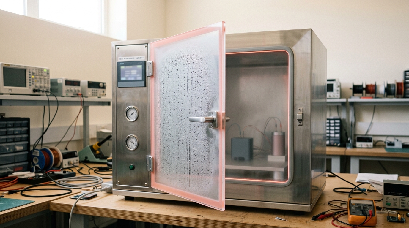
The same distinction between lab benchmark and field performance applies to compute, not only to sensing. MLPerf Tiny’s own design brief is explicit that accuracy, latency, and energy have to be measured together, on standardized reference tasks, precisely because a part that looks efficient on a synthetic microbenchmark can behave very differently once real duty-cycling, thermal throttling, and memory-access patterns from an actual deployed workload are introduced [2]. Neither of these citations proves that field reliability is solved; both establish that the size of the lab-to-field gap is measurable, has been measured in at least these documented cases, and is not a fixed cost that model or chip design has no leverage over.
Three scenarios for 2035
Scenario A — incremental compounding.
Scenario B — an in-memory or neuromorphic discontinuity. Compute-in-memory silicon, or a comparably disruptive alternative to digital CMOS switching, clears the manufacturability and yield bar that has so far kept it in research and niche deployments, and
Scenario C — fragmented, regulation-led divergence. Jurisdictions diverge sharply on AI-specific privacy law, and on-device, privacy-by-architecture designs become mandatory in some major markets (the EU being the most likely first mover given the AI Act’s existing structure) while remaining optional elsewhere, producing genuinely different edge hardware and software stacks by region rather than one converging global design point. This assumes enforcement and implementing guidance under the AI Act — not yet written in the detail this scenario requires — moves toward architecture-specific requirements rather than staying purely outcome-based.
These scenarios are not mutually exclusive, and the predictions below are deliberately narrower and more falsifiable than any one of them, because a scenario this coarse cannot itself be disconfirmed by a single observation.
Predictions, and what would falsify each one
Prediction one — the power-per-inference gap narrows but does not close. Horizon: 2035. Assumption: no in-memory or neuromorphic discontinuity reaches high-volume manufacturing at competitive cost before then. Claim: the achievable energy-per-inference on the best shipping edge silicon for a fixed benchmark task (comparable to MLPerf Tiny’s suite, or its 2035-era successor) will have improved by roughly one to two orders of magnitude relative to 2025-era parts, driven mainly by architecture and quantization rather than by a change in switching physics. Observable indicator: successive MLPerf Tiny-style result rounds through the early 2030s show efficiency gains slowing on a log scale, consistent with an asymptote rather than a fresh exponential. Disconfirmed if a compute-in-memory or comparable non-digital-switching architecture accounts for the majority of the highest-efficiency submissions in that benchmark class by 2032, which would indicate Scenario B rather than Scenario A actually occurred.
Prediction two — event cameras and neuromorphic processing stay a fitted niche, not a general replacement. Horizon: 2035. Assumption: no single application category grows large enough to fund a general-purpose event-vision pipeline competitive with conventional CMOS imaging on cost per unit. Claim: event-camera and spiking-neuromorphic components will be present in a meaningfully larger set of shipping industrial, automotive-adjacent, and always-on-sensing products than today, but will not have displaced conventional frame-based cameras and dense accelerators as the default sensing-and-compute pairing for general-purpose vision tasks. Observable indicator: unit shipment or design-win disclosures (to the extent vendors report them) remain concentrated in industrial monitoring, automotive perception subsystems, and low-power wake sensing rather than broadening into consumer general-purpose cameras. Disconfirmed if a mainstream consumer device category (phones, mainstream AR devices, or general laptops) adopts an event-camera-plus-neuromorphic pipeline as a primary rather than auxiliary sensor by 2035.
Prediction three — privacy-preserving on-device inference becomes a de facto requirement in at least one major regulatory jurisdiction, short of universal legal mandate. Horizon: 2032, ahead of the full 2035 horizon because AI Act implementation milestones fall within this window. Assumptions: the EU AI Act’s phased implementation continues on its current published timeline through 2027 and beyond, and no major jurisdiction reverses course on AI-specific data-governance obligations. Claim: by 2032, satisfying high-risk-tier data-governance and documentation obligations under AI-specific regulation in at least one major jurisdiction will be measurably cheaper and lower-risk for an on-device, privacy-by-architecture design than for a design that transmits raw personal data off-device for inference, even though no such regulation will explicitly mandate on-device processing by name. Observable indicator: published compliance guidance or enforcement actions that specifically credit data-minimizing, on-device architectures as reducing obligations under high-risk-tier rules. Disconfirmed if by 2032 regulatory guidance and enforcement remain fully architecture-neutral, treating on-device and off-device designs as equivalent so long as stated outcomes (documentation, oversight, accuracy) are met.
Prediction four — a compute-in-memory or comparable discontinuity reaches commercial volume for at least one significant device class, but not for general-purpose edge inference broadly. Horizon: 2035. Assumption: the specific engineering blockers visible in today’s research chips — device-to-device variability, write endurance, and cost per bit relative to mature digital memory — are solvable at commercial volume for at least one application, even if not for all of them. Claim: by 2035, at least one shipping product category (most plausibly a narrow, high-value, power-constrained niche such as an implantable or industrial-safety sensor rather than a mainstream consumer chip) will use analog or compute-in-memory silicon as its primary inference engine rather than as a research demonstration. Observable indicator: a named commercial product, not a research prototype or a press-release roadmap claim, ships with in-memory or analog compute as its documented primary inference path. Disconfirmed if by 2035 every publicly known compute-in-memory or comparable effort remains at the research-chip or pilot-line stage with no shipping commercial product built around it as the primary inference engine.
What to take away
Nothing above requires believing in an inevitable breakthrough or an inevitable plateau; both are scenarios, not facts, and the honest position is that the evidence in hand supports either, conditioned on assumptions this piece has tried to state rather than bury. What the evidence does support as closer to settled: the power budget on an edge device is close to fixed by the product category, so essentially all growth in on-device capability between now and 2035 has to come from growth in efficiency rather than from simply spending more power; that efficiency growth inside conventional CMOS faces a real, documented, asymptotically approached floor; that event-camera and neuromorphic sensing already work exactly as well as the peer-reviewed literature says they do, on exactly the narrow class of problems that literature has actually tested; that today’s privacy regulation is real but architecture-neutral on its face, with the harder architectural mandate still a scenario rather than settled law; and that the gap between a laboratory benchmark and a field-deployed sensor or model is itself a measured, closeable quantity rather than an excuse. Four dated predictions follow from those facts, each one built to be provably wrong by a specific date if the evidence between now and then says so.