An idea the industry gave up on
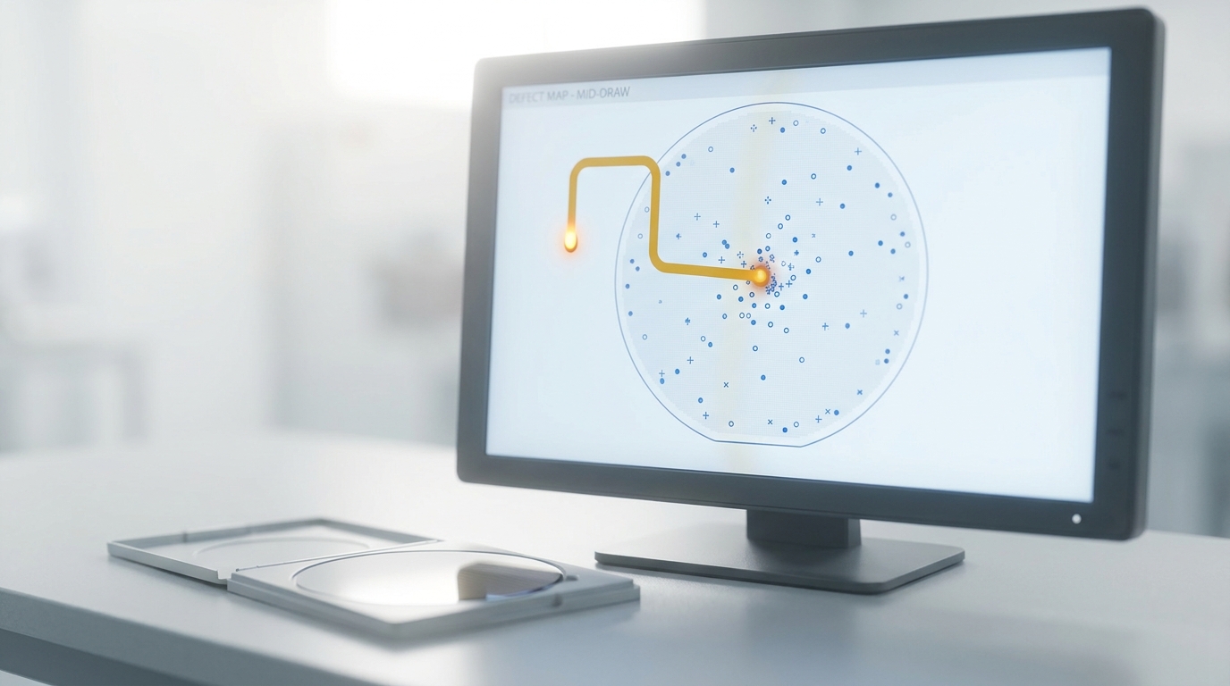
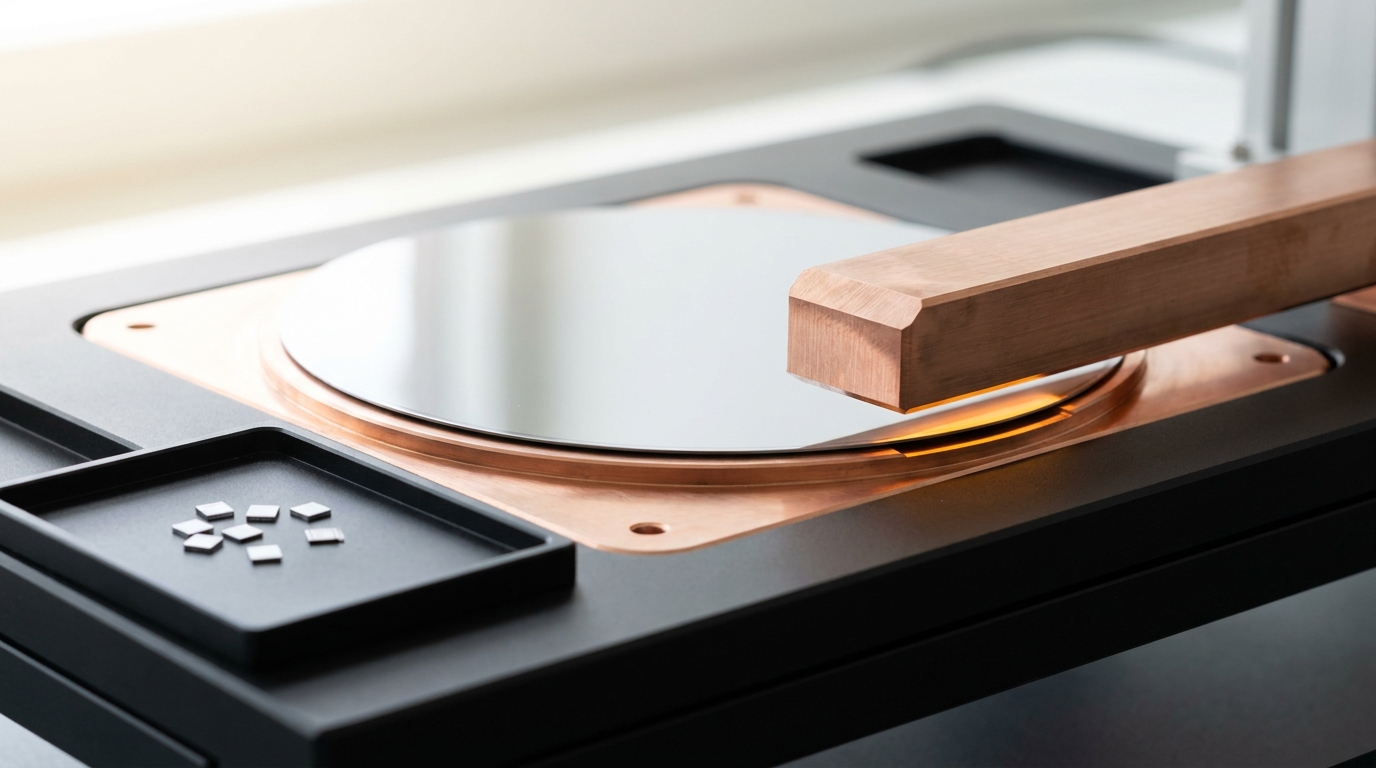
Wafer-scale integration — building one processor out of an entire uncut silicon wafer, instead of dicing the wafer into many separate chips — was seriously attempted in the 1980s and largely abandoned, for a simple reason: the larger the piece of silicon, the more likely it is to contain at least one manufacturing defect, and a single defect anywhere on an undivided wafer could disable the entire chip. Ordinary chip manufacturing solves this by cutting the wafer into small dies, so one flawed die can be discarded while its neighbors ship normally. Cerebras’s core engineering bet is that this old, abandoned idea can work after all, given the right architecture.
How Cerebras actually solves the defect problem
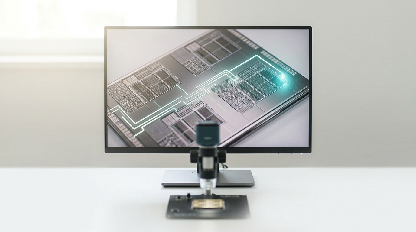
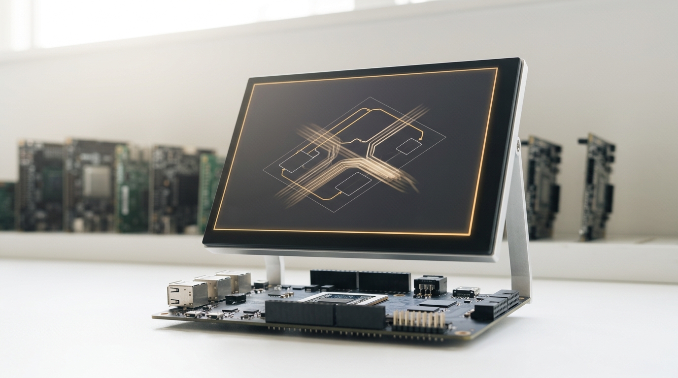
Rather than treating a defect as fatal to the whole part, Cerebras’s architecture is designed to route around flawed regions of the wafer, using redundant compute elements and reconfigurable interconnects so a manufacturing defect disables a small local area rather than the entire chip. This is the specific engineering breakthrough that makes wafer-scale integration commercially viable now in a way it wasn’t in earlier attempts — the defect-tolerance problem is solved at the architecture level rather than requiring impossibly perfect manufacturing across an entire wafer’s surface area.
What wafer-scale actually buys a customer
The practical payoff is enormous on-chip memory bandwidth and an entire model’s working set kept physically close together on one piece of silicon, avoiding the chip-to-chip communication overhead that dominates large multi-GPU training and inference clusters. Independent comparisons of Cerebras against Groq and SambaNova — the other leading non-GPU inference architectures covered elsewhere in this cohort — generally describe Cerebras’s advantage as most pronounced on workloads that benefit from that specific property: very large models where cross-chip communication would otherwise be the bottleneck [3].
The commercial validation
Cerebras’s reported OpenAI partnership, valued at more than $10 billion, is the clearest evidence that the wafer-scale approach has moved from an interesting architecture to a workload customers are willing to commit serious money to [2]. Combined with the company’s successful May 2026 IPO — covered in this cohort’s companion piece — Cerebras has now cleared both major validation hurdles a hardware startup faces: a customer willing to commit meaningful revenue, and a public market willing to price the business at a serious valuation.
The risk this architecture still carries
Wafer-scale integration’s core advantage — an entire model’s working set close together on one wafer — is also its core limitation: a wafer-scale chip is a fixed, enormous, expensive unit that cannot be incrementally scaled the way adding one more GPU to a cluster can. A customer commits to Cerebras’s specific architecture at a coarser granularity than a conventional GPU cluster, which concentrates both the upside and the risk of the bet in a way this cohort’s other inference- architecture briefings, covering more incrementally scalable approaches, generally do not share to the same degree [4].
Why manufacturing a wafer-scale chip is its own engineering feat
Beyond the architectural defect-tolerance problem already described, simply manufacturing and packaging a chip this large introduces problems ordinary chip production never has to solve: thermal expansion across a much larger area during manufacturing and operation, power delivery uniform enough across the entire wafer’s surface that no region starves for current, and cooling capacity sufficient to remove heat from a single enormous die rather than distributing that load across many smaller, individually cooled packages. Cerebras has had to develop custom manufacturing, packaging, and cooling solutions for essentially every step of this process, since no existing supply chain — built entirely around ordinary diced chips — offered an off-the-shelf answer for any of it.
How the IPO changes the calculus for wafer-scale as a category
With Cerebras now a public company, its wafer-scale bet is subject to a level of ongoing financial scrutiny — quarterly revenue disclosure, customer concentration reporting, capital efficiency comparison against peers — that a private company never faces to the same degree. That scrutiny cuts both ways for the wafer-scale approach as a whole: sustained, visible commercial success would validate wafer-scale integration as a durable architectural category rather than a one- company curiosity, potentially drawing new entrants or renewed research investment into the approach; a visible stumble would just as publicly reinforce the industry’s decades-old skepticism about whether wafer-scale integration can ever be more than a niche solution for the handful of workloads it suits best.