TSMC Starts Shipping This Year. Samsung’s Bonded Version Waits Until 2027, Its Turnkey Version Until 2029
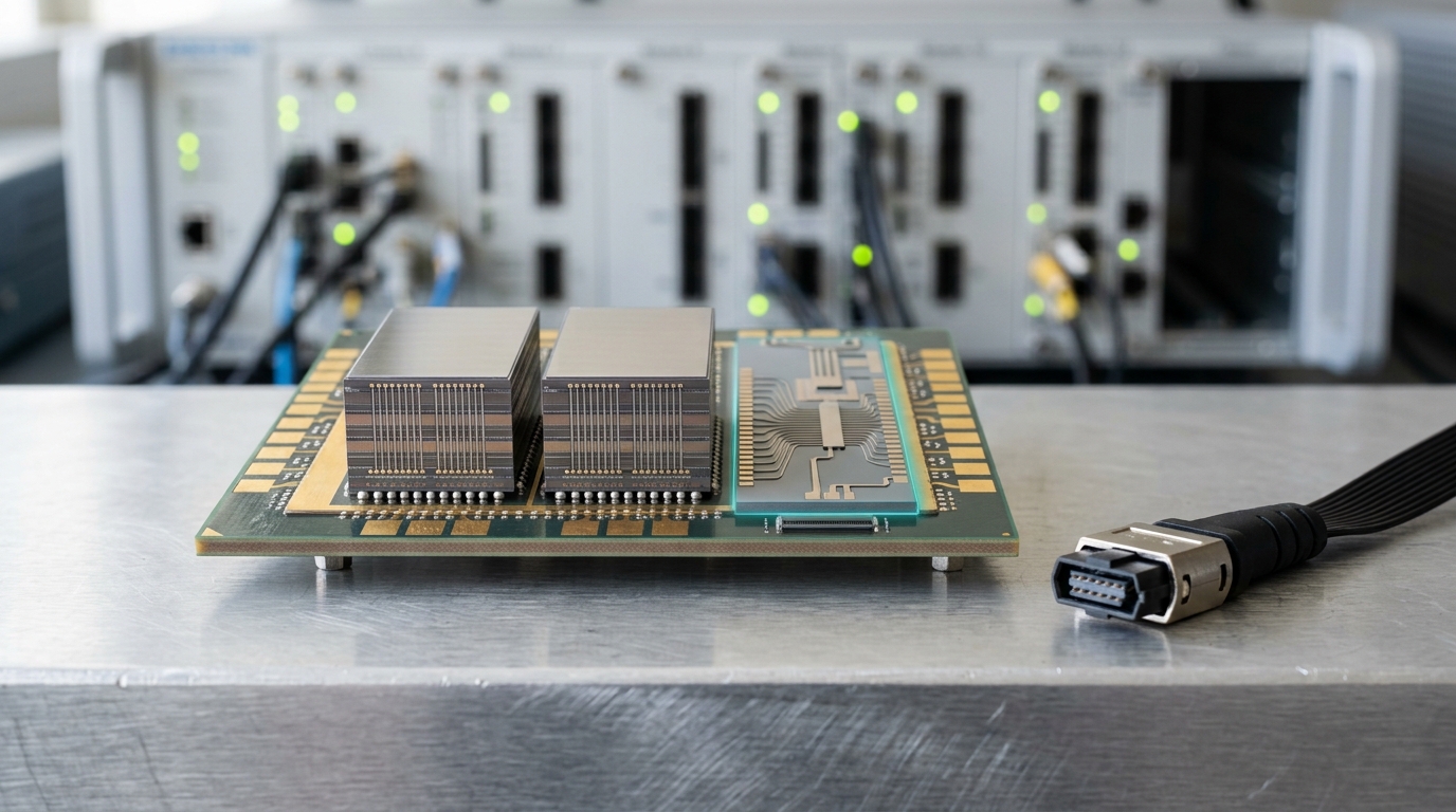
Every switch vendor building the next generation of AI-cluster networking wants the same part: a chip that puts light-emitting and light-detecting components right next to the logic driving them, so a multi-terabit switch doesn’t spend a third of its power budget pushing electrical signal out to pluggable optical modules bolted onto a faceplate. That part is called co-packaged optics, and in 2026 it stopped being a laboratory demonstration and became a line item on four separate companies’ published roadmaps: TSMC, Samsung Foundry, GlobalFoundries, and imec. The claim in this piece is narrower than “co-packaged optics is coming,” and more checkable. These four roadmaps do not describe one technology converging on one date. They describe four different, physically distinct answers to a single engineering question — where, exactly, does the electronic die actually meet the photonic die? — arriving on schedules that are not close to each other, and the size and shape of that scheduling gap, not any dispute about the underlying physics, is what will decide which company’s version becomes the industry’s shared socket first.
Start with the two companies that have put an actual number on a calendar. TSMC’s COUPE platform — the name expands to Compact Universal Photonic Engine — is “set for volume production this year,” meaning 2026, with CoWoS-based co-packaged-optics integration also targeted for 2026 and qualification of small-form-factor pluggable modules using the same underlying technology targeted a year earlier, in 2025 [1]. Samsung Foundry’s answer to the same question is not one date but two, and the industry’s habit of quoting only one of them is the first thing this piece has to correct. Samsung’s optical engines, built using thermo-compression bonding, are planned for 2027. Samsung’s turnkey co-packaged-optics service — the point at which Samsung can hand a customer a finished CPO product rather than one component in someone else’s assembly — is not targeted until 2029, on a 300-millimetre wafer process [1]. Anyone who reports “TSMC 2026 versus Samsung 2029” has picked the widest possible version of that gap without saying so. Anyone who reports “TSMC 2026 versus Samsung 2027” has picked the narrowest version without saying so either. Both numbers are real, and which one is the operative comparison is exactly the kind of question a scheduling-gap story cannot skip past.
The reason any of this is worth a hyperscaler’s attention rather than a packaging engineer’s alone is a number TSMC itself has put in front of customers: moving a switch’s interconnect from copper wire to co-packaged optics offers “more than 10X power benefit,” according to TSMC’s own COUPE materials as reported from the platform’s public technical briefings [5]. That is a vendor’s own claim, stated here as a claim rather than an independently reproduced measurement — nobody outside TSMC has published a component-level budget that adds up to the same number — but it is the specific number that explains why three large companies and one research institute are all racing toward the same merged package rather than continuing to ship pluggable optical modules the way the industry has for two decades. This piece is not that budget. A companion piece elsewhere in this publication’s semiconductor coverage, Nvidia and the Bet on Light, Not Copper, covers one buyer’s adoption decision and the liquid-cooling dependency that decision forces; a separate piece, Ayar Labs and the Optical I/O Problem, covers one startup’s connector-chip thesis built on the same underlying demand. Neither asks the question this piece asks, which is not whether co-packaged optics is coming or who wants it, but which company’s specific process actually merges the two dies first, second, and last, and by how much.
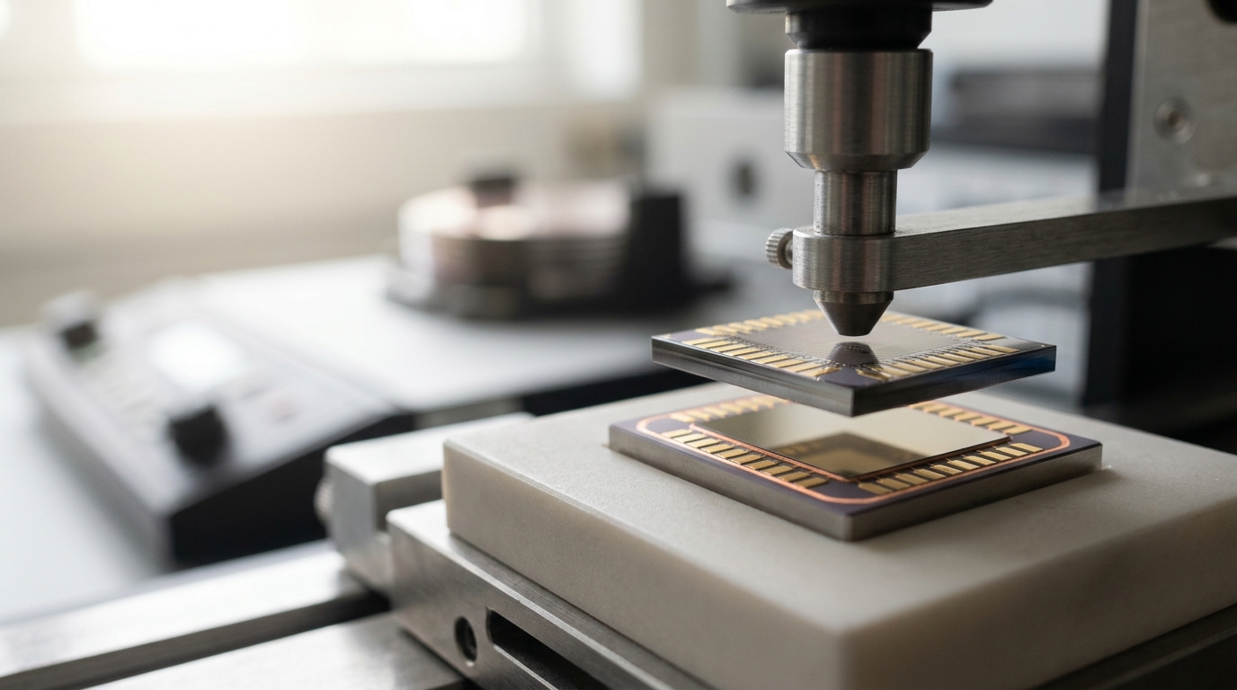
Silicon photonics itself is not a new field — it names the use of silicon as an optical medium, typically patterned at sub-micron precision and operated at the 1.55-micrometer wavelength standard to fiber-optic telecommunications, built on a silicon-on-insulator structure [6] — and that maturity is exactly why “four companies are all building CPO now” undersells what’s actually new. The optical physics has been demonstrated for years. What changed between roughly 2024 and 2026 is that the specific process step of merging an electronic control die with a photonic die stopped being a research question and became four separate, publicly dated (or deliberately undated) engineering commitments.
Only Two of the Names in This Race Are Actually Foundries in the Old Sense
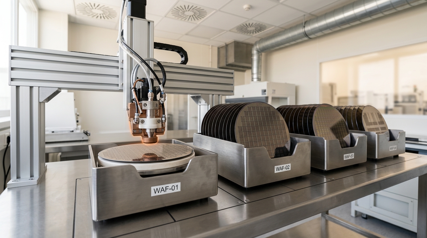
I want to slow down on a slippage the framing above already contains, because it is this piece’s actual first claim, not throat-clearing before the real argument starts. TSMC and Samsung are foundries selling a captive, proprietary manufacturing process. You get a COUPE-stacked chip by being a TSMC customer who commits to TSMC’s process; you get a thermo-compression-bonded optical engine by being a Samsung Foundry customer who commits to Samsung’s. Neither company publishes the process details a competitor would need to reproduce the bond. GlobalFoundries’ silicon-photonics business is also a foundry offering, but a differently shaped one — not a single date on a single roadmap slide, but three already-built generations of a native process technology that was never trying to win a specific calendar race to begin with, plus a packaging platform layered on top of the third generation. And imec is not a foundry selling a manufacturing process at all. It is a nonprofit research institute that sells shared access to one, through the same multi-project-wafer model that has funded photonics prototyping for over a decade, long before TSMC or Samsung announced a photonics product roadmap [8].
That distinction matters because the dossier framing behind this piece — “three foundries… on three different clocks” — only survives if you read “three clocks” correctly. TSMC keeps one. Samsung keeps one, or rather two, as the previous section just showed. GlobalFoundries keeps a process-generation ladder rather than a single production date, which is its own kind of clock, slower and less legible than the other two. imec was never running a clock in this sense at all, because a research-access foundry doesn’t announce when its customers’ products ship — its customers do that, on their own schedules, using imec’s process as one input among several. Treat all four as identical points on one timeline and the comparison collapses into exactly the kind of “the industry is converging” narrative this piece exists to replace with something more specific. Keep the distinction and a genuinely useful taxonomy falls out of it almost by itself: two proprietary product roadmaps running on different clocks, one proprietary process ladder running on no single publicly stated date, and one open research platform that isn’t in the race in the same sense the other three are.
GlobalFoundries Already Has Three Generations Running While Nobody Was Watching
GlobalFoundries’ own technology page states its silicon-photonics history as three generations, each described in specific, checkable numbers rather than a marketing adjective. Generation 1 “delivers production-proven, high-volume capability to support up to 100G/λ” with flexible channel spacing between 100 and 400 gigahertz and 55 gigahertz of usable bandwidth. Generation 2 is “proven up to 200G/λ with significant bandwidth upgrades (>65GHz), 200GHz channel spacing,” aimed at more advanced modulation formats. Generation 3 offers, in GlobalFoundries’ own words, “a clear path to 400G/λ, optimized for scale across data center architectures,” and is currently available on early access rather than general production [2]. Layered on top of Generation 3 is a packaging platform called SCALE, which GlobalFoundries describes as “the industry’s first OCI MSA-capable platform, exceeding requirements for the interconnect specification for modern AI scale-up architectures” [2] — a claim about meeting an external interconnect specification rather than a claim about a specific ship date, which is worth noticing precisely because it is a different kind of claim than TSMC’s or Samsung’s.
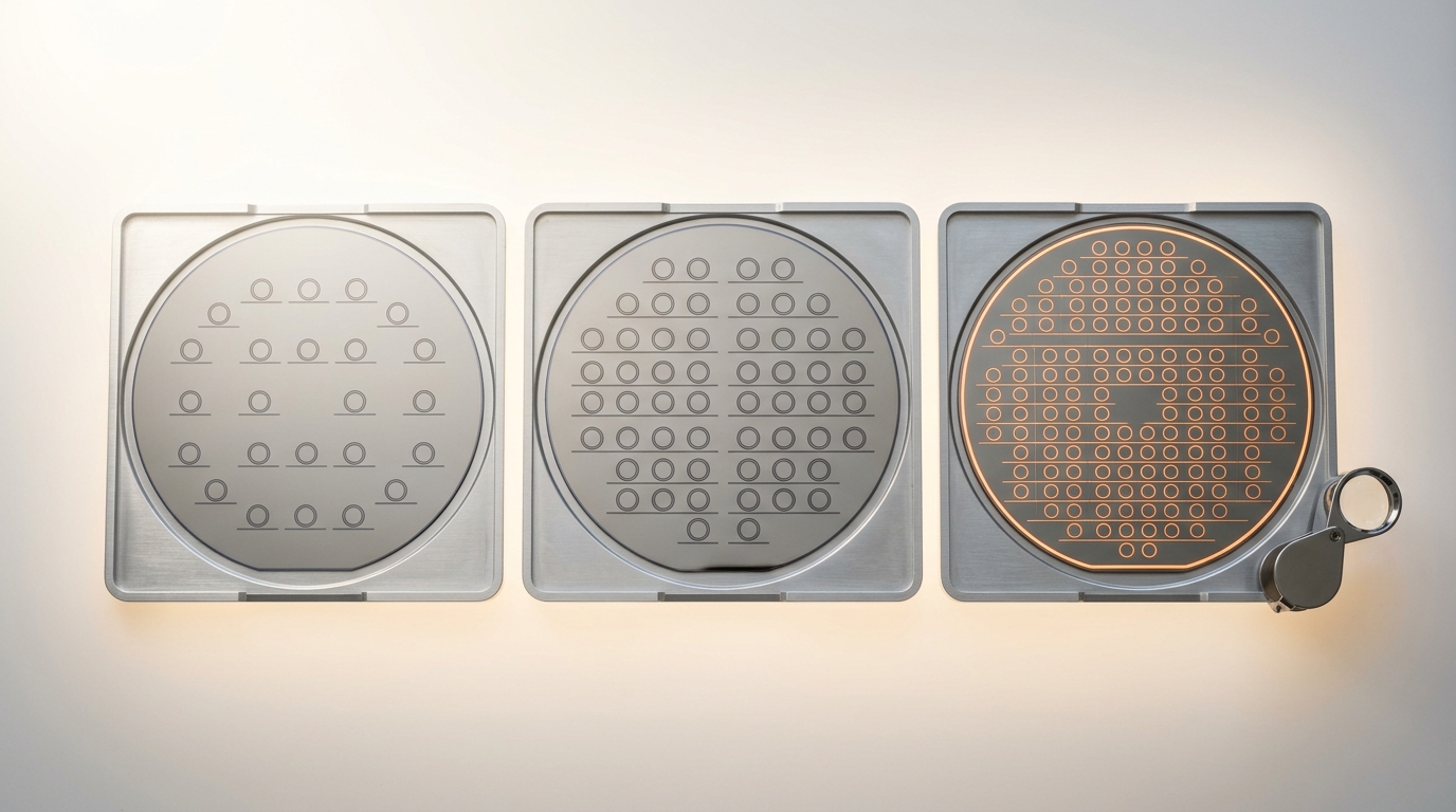
Notice what is missing from that paragraph and what its absence means. GlobalFoundries’ own materials, read directly rather than through secondary coverage, do not state a volume-production year for SCALE the way TSMC states 2026 or Samsung states 2027 and 2029. That could mean GlobalFoundries is further behind and declining to say so. It could equally mean GlobalFoundries considers “early access on Generation 3, packaged through SCALE” itself the operative milestone, with volume following customer qualification on a schedule GlobalFoundries doesn’t control unilaterally the way TSMC and Samsung appear to for their own captive platforms. Both readings are consistent with the same public evidence, and a comparison that quietly resolves that ambiguity into “GlobalFoundries is behind” without saying so is doing exactly the kind of unearned resolution this piece is built to avoid. The honest statement is narrower: GlobalFoundries has three built, characterized process generations and a packaging platform aimed at a named interconnect specification, and no publicly stated volume date comparable to the other two companies’ numbers. That is a gap in the public record, not a finding about GlobalFoundries’ actual production timeline, and the two should not be confused with each other.
An objection worth stating before it gets raised by a reader instead: isn’t “no stated date” just a polite way of saying “further behind,” dressed up as methodological caution? Not necessarily, and the reason is structural rather than charitable. TSMC’s and Samsung’s numbers describe a single proprietary product line each is fully responsible for shipping on its own schedule. A multi-source interconnect specification — the category GlobalFoundries places SCALE in — depends by definition on more than one company agreeing to build against the same interface, the way earlier pluggable-optics interoperability agreements let switch vendors, module makers, and cable assemblers ship compatible parts without one company controlling the whole stack. A platform built around meeting a shared specification genuinely cannot publish a unilateral ship date the way a captive stack can, because part of what “compliant” means is waiting on other companies’ silicon too. That structural difference is a real possible explanation for the missing date, not proof of one; the honest position is that the public record checked for this piece cannot distinguish “GlobalFoundries is behind” from “GlobalFoundries is building the one platform whose date isn’t fully its own to set,” and a comparison that resolves that ambiguity in either direction without saying so is asserting more than the evidence supports.
imec Never Set a Production Date, Because imec Isn’t Selling a Product
imec’s two current platforms make the “research institute, not a foundry” distinction concrete rather than definitional. iSiPP200, its mature 200-millimetre offering, comes with what imec calls “a comprehensive silicon-validated PDK” — a process design kit whose device models have actually been checked against fabricated silicon, the specific claim that separates a usable foundry service from a research curiosity. That platform gets its lasers onto silicon two ways: flip-chip bonding at wafer scale, where a separately grown III-V laser die is picked up, flipped face-down, and pressed onto matching bond pads on the silicon photonic chip; and micro-transfer printing, where a stamp lifts a much smaller device “coupon” off a source wafer and prints it down at a placement density flip-chip bonding cannot match, used specifically for integrating lithium-niobate modulators, III-V lasers, and semiconductor optical amplifiers [3].
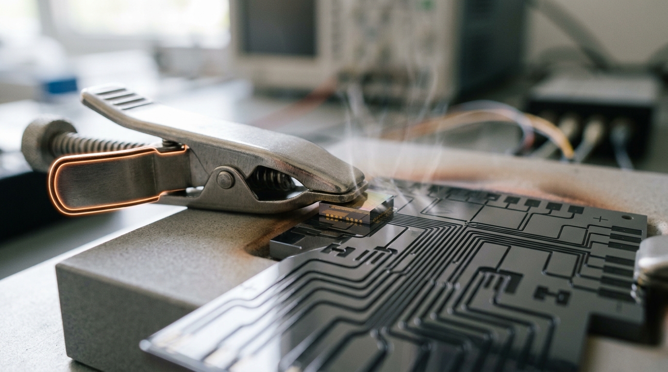
The stamp analogy is useful and it has a limit worth stating before it does any more work in this piece. A rubber stamp presses ink onto paper without needing to land within a fraction of a micron of a target and without caring whether any ink is left behind on the stamp afterward. A micro-transfer-printing stamp has to place a device coupon with sub-micron accuracy onto exact bond sites, and the residue it leaves — or fails to leave — behind on the source wafer determines whether the process can run at production yield rather than one-off in a lab. Where the analogy holds: both methods move a small, complete object from one surface to another in a single motion. Where it breaks: the stamp’s job is precision transfer at device scale, not bulk marking, and that difference is the entire reason imec runs both flip-chip and micro-transfer printing side by side rather than treating one as simply the newer replacement for the other — each suits a different device size and yield target.

imec’s newer platform, iSiPP300, moves to 300-millimetre wafers and adds exploratory features including through-silicon vias, microbumps, and embedded microbumps — process capability that looks toward denser 3D integration without yet being the mature, silicon-validated offering iSiPP200 is. It has already produced one specific, checkable result: a “beyond-110GHz C-band GeSi electro-absorption modulator,” confirmed directly against imec’s own published platform description rather than taken on a secondary source’s word [3] — a modulator bandwidth figure the dossier behind this piece had flagged as unconfirmed going into drafting, and which a direct read of imec’s own materials resolves. Neither iSiPP200 nor iSiPP300 comes attached to a stated production-volume year, and that absence is not an oversight in imec’s public communications. A research-access foundry’s customers set their own production schedules once they leave imec’s process; imec’s job ends at qualified silicon, not at a shipped product, which is the structural reason it was never going to publish a date comparable to TSMC’s or Samsung’s in the first place.
The Widest Gap Isn’t Between the Fastest and Slowest — It’s Between Two Numbers Samsung Itself Published
Put TSMC’s and Samsung’s numbers next to each other precisely and a sharper picture appears than the “TSMC 2026, Samsung 2029” version usually reported. TSMC’s volume-production target and Samsung’s optical-engine target are one year apart: 2026 against 2027. TSMC’s volume-production target and Samsung’s full turnkey-service target are three years apart: 2026 against 2029. Those are not two ways of stating the same fact with different rounding. They are two different milestones — a bonded component reaching production versus a complete, sellable CPO service reaching customers — and Samsung’s own roadmap treats them as genuinely separate events, not stages of one smooth ramp reported at different times. A comparison that quotes only 2029 is not wrong, but it is comparing TSMC’s earliest stated milestone to Samsung’s latest one, which makes the gap look categorical when the underlying evidence supports something closer to “close on the first milestone, still far apart on the second.”
| Platform | Where the electronic and photonic dies actually merge | Native process reach | Stated milestone(s) |
|---|---|---|---|
| TSMC COUPE | 3D SoIC-based stacking: a logic die stacked directly on a photonic die to form one “optical engine” [1] [5] | — | Volume production 2026; small-form-factor pluggable qualification 2025 [1] |
| Samsung Foundry | Thermo-compression-bonded optical engine, followed by a turnkey CPO service | 300mm | Bonded optical engines 2027; full turnkey service 2029 [1] |
| GlobalFoundries | Native silicon-photonics process (Gen1 → Gen3) plus SCALE advanced-packaging layer | Gen3: path to 400G/λ | Gen3 on early access; no stated volume-production year [2] |
| imec | Flip-chip bonding and micro-transfer-printed III-V-on-silicon, open foundry-service access | 200mm mature / 300mm exploratory | No production date — a research-access platform, not a product roadmap [3] |
Reading that table by column rather than by row is the point. Read by row, it looks like four competitors on a track, spaced out at the gun. Read by column, the “stated milestone” cells are answering different questions for different rows — a shipping date for two of them, a process-maturity marker for the third, nothing at all for the fourth because the question doesn’t apply to a research-access foundry the way it applies to a product line. Treating all four cells as comparable timeline entries is the specific mistake a scheduling-gap story has to avoid making, and it’s the mistake the “TSMC versus Samsung versus GlobalFoundries versus imec, five-plus years apart” framing risks making if the table is read the easy way instead of the honest one.
A Later Start Doesn’t Automatically Lose the Socket
None of this should be read as a prediction that TSMC wins because it ships first. A foundry with a later stated date can still win the eventual standard-setting position if its process delivers materially better yield or lower fiber-to-chip coupling loss than an earlier-arriving competitor’s — first-to-ship and first-to-be-adopted-at-scale are different races, and conflating them is a second, independent way this kind of comparison goes wrong even after the scheduling-gap point above has been correctly made. Samsung’s decision to separate “bonded optical engine” from “turnkey service” by two years could reflect exactly this kind of deliberate yield-hardening step rather than a simple delay, and the public record checked for this piece does not distinguish between those two explanations. Stating that limit plainly is more useful than picking a winner the evidence doesn’t support.
It is worth closing the historical loop this piece opened with, because it sharpens the actual verdict rather than just restating it. Silicon photonics has an older, still-functioning access model that predates every one of the four platforms compared above: AIM Photonics, a federally backed manufacturing institute founded in 2015, released an integrated silicon-photonics process design kit through the same shared, multi-project-wafer model imec still uses, giving members “a library of photonic components designed to work within the SUNY Poly silicon photonics process” and space on shared wafer runs scheduled the following year [4] [7]. That model — open access, shared cost, a common process design kit, no single company’s production calendar attached to it — is not a relic. It still runs, at imec and elsewhere, and it is exactly the kind of platform the word “silicon photonics” used to bring to mind by default: a research capability, not a product line with a ship date. The reason this piece’s verdict describes 2026 as the year the field “stopped being a research platform and became a foundry roadmap item” is not that the open-access route disappeared. It is that TSMC and Samsung now publish production years the way any other advanced-packaging product line does, GlobalFoundries has three built generations behind a named commercial platform, and the open, shared-access model that used to be the field’s entire public face is now the background infrastructure sitting behind those three commercial roadmaps rather than standing in for the whole field the way it once did.
What Would Prove This Wrong Within a Year
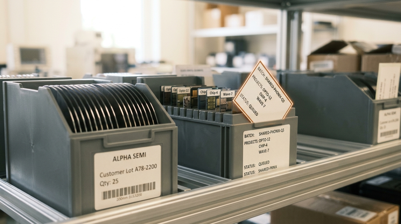
State the failure condition precisely enough that it could actually fail. If, within twelve months of this piece’s publication — meaning by roughly September 2027 — two or more of TSMC, Samsung, and GlobalFoundries ship qualified volume co-packaged-optics product within the same calendar year, the “scheduling gap decides who owns the socket” framing collapses into a simultaneous-arrival story instead, and this piece’s central claim would need to be withdrawn rather than defended. That window is closer than the naive 2026-versus-2029 comparison makes it look: Samsung’s own bonded-optical-engine milestone lands in 2027, the same twelve-month window this falsifier covers, so if GlobalFoundries’ Generation 3 platform reaches a comparable volume milestone in that same window — a real possibility the public record neither confirms nor rules out, given GlobalFoundries has stated no date at all — the three companies that do keep a calendar could plausibly converge within the falsification window this piece itself set, not years past it. A second, narrower failure condition applies to the imec comparison specifically: if imec’s foundry-service customers begin publishing their own volume-production years for imec-fabricated co-packaged-optics products at a pace comparable to TSMC’s or Samsung’s captive roadmaps, the claim that imec “was never running a clock in this sense” would need qualification, since a research-access platform whose customers routinely hit product dates on schedule starts to function like a fourth clock in practice even without imec itself publishing one.
What changes if the framing holds instead is specific enough to act on rather than merely interesting to read, and it changes differently depending on which side of the table a reader sits on. A hyperscaler large enough to co-design silicon with TSMC directly is choosing a 2026 stacked-die commitment now, on TSMC’s terms, with the power-efficiency claim above as the number it is buying against. A switch vendor without that kind of leverage is more likely shopping GlobalFoundries’ or a comparable merchant foundry’s packaging platform precisely because it depends on a shared specification rather than a single captive customer relationship — the same reason the pluggable-optics era let smaller vendors ship compatible parts at all. And a startup or university lab with a photonic device idea and no foundry relationship at all is still, in 2026, most likely to reach silicon through exactly the open, shared-access route this piece traced back to 2016 — imec’s iSiPP platforms or a comparable multi-project-wafer program — because that route, not any of the three captive roadmaps, remains the one place a small, unproven idea can buy space on a production-grade wafer without first becoming one of TSMC’s or Samsung’s named customers. All three of those readers are looking at the same set of four platforms and correctly reaching three different conclusions about which one matters to them, which is itself evidence that “co-packaged optics has arrived” is too coarse a sentence to guide a real decision no matter which side of the table it is read from.
Reading past those differences to write “co-packaged optics arrives in the second half of the decade” is not wrong so much as it is the wrong grain of resolution for a decision that actually has to be made against one company’s specific date, not the industry’s averaged one.