The question asked confidently, and answered wrong
Ask who invented the transistor and most people reach for one name: William Shockley — brilliant, difficult, later infamous well beyond electronics. The documented fact undercuts the single-name story immediately. Shockley was not in the room on 16 December 1947, when John Bardeen and Walter Brattain got a sliver of germanium wired to two gold contacts to amplify an electrical signal for the first time, in a Bell Telephone Laboratories workshop at Murray Hill, New Jersey [2]. Shockley first saw the device work a week later, on 23 December, when Bardeen and Brattain demonstrated it to laboratory management — and reportedly called it “a magnificent Christmas present” [2].
That much is not seriously disputed. What is disputed, endlessly, in popular histories and online arguments alike, is who “really” deserves the credit. The honest answer is that the question rests on a false premise. There were two transistors, invented about six weeks apart on different physics, and the industry now runs almost entirely on the second one.
What actually happened on 16 December 1947
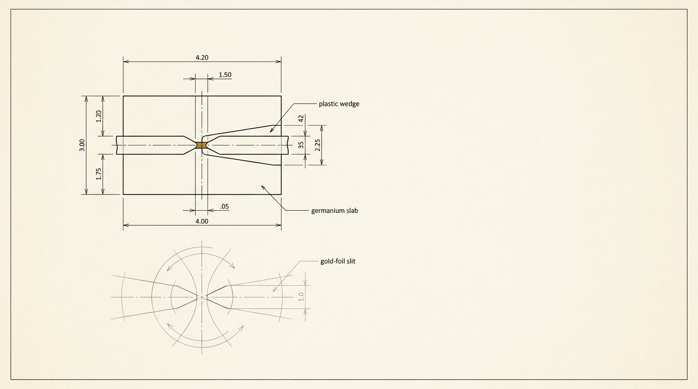
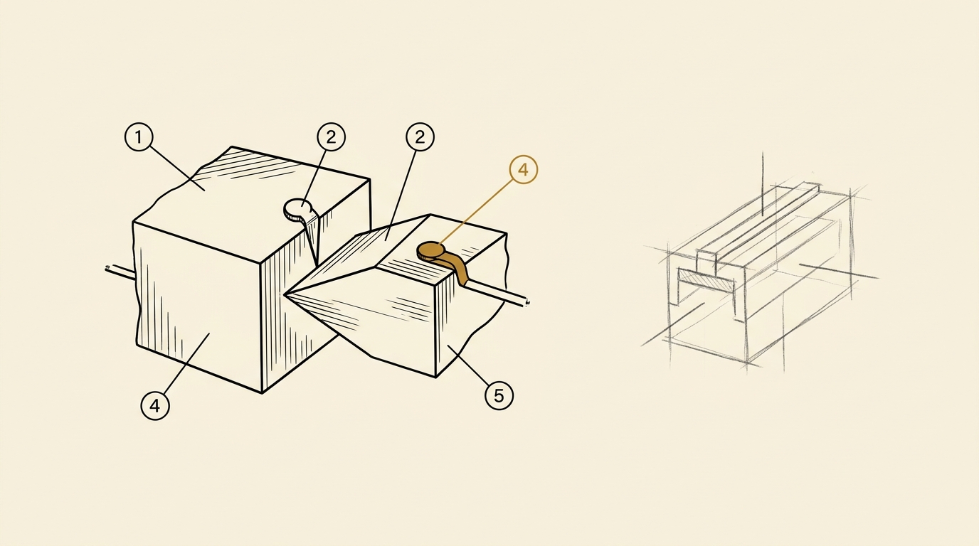
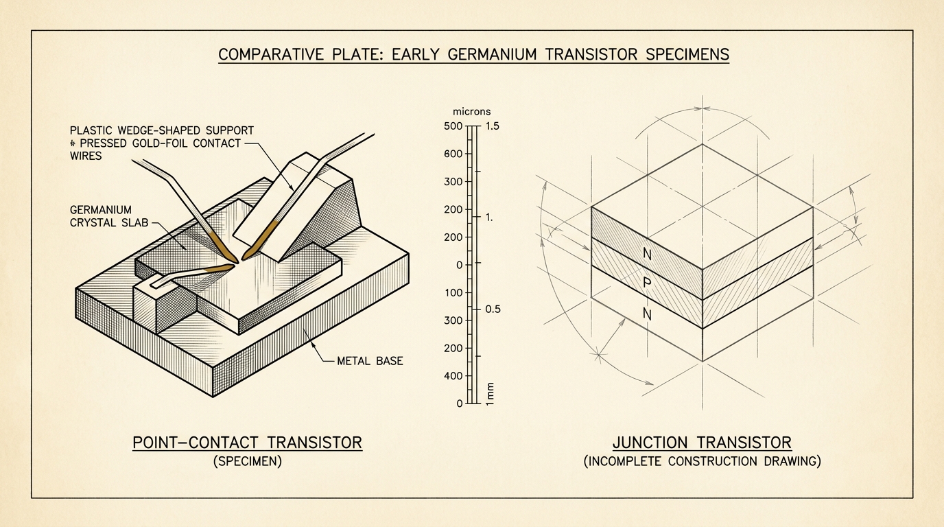
The device Bardeen and Brattain got working that night was a point-contact transistor: a small block of high-purity germanium, a wedge of plastic, and a strip of gold foil that Brattain had cemented to the wedge’s point and then sliced with a razor blade, creating two contacts separated by roughly the thickness of a sheet of paper [2]. Pressed onto the germanium’s surface, the two contacts let a small voltage on one control a much larger current through the other — amplification, without a vacuum tube, a filament, or any warm-up delay [2]. Bardeen supplied the theory, built around his research into “surface states” — the idea that electrons trapped at a semiconductor’s surface were blocking the electric fields that Shockley’s own, earlier field-effect designs had depended on and repeatedly failed to demonstrate. Brattain supplied the hands.
Why the patent could not carry Shockley’s name
Shockley wanted credit, and reportedly told Bardeen and Brattain separately that he could write a patent covering the whole invention starting from his own, earlier field-effect theory [7]. Bell’s patent attorneys overruled him. Searching prior art, they found that a Brooklyn-based physicist named Julius Lilienfeld had already patented the core idea of controlling current through a solid with an external field two decades earlier — one patent filed in 1926 and granted in 1930, a second filed in 1928 and granted in 1933 — even though no evidence survives that Lilienfeld ever built a working device from either [4]. Attaching Shockley’s field-effect claim to the new patent risked the entire filing being invalidated by Lilienfeld’s prior art. So the attorneys filed narrowly, on the specific mechanism Bardeen and Brattain had actually built and that Lilienfeld’s paper patents had not anticipated: “Three-Electrode Circuit Element Utilizing Semiconductive Materials,” U.S. Patent 2,524,035, naming only Bardeen and Brattain, filed in June 1948 and granted in October 1950 [5]. Shockley’s name is absent from it — not because his contribution to the underlying science was disputed, but because his specific theoretical claim was judged unpatentable next to Lilienfeld’s.
The transistor Shockley built instead
Shockley did not take the exclusion well. Within weeks he had worked out, on paper, a fundamentally different device — one built on a junction between differently doped regions of a single germanium crystal, rather than two mechanically pressed metal points, extending the p-n junction work Russell Ohl had done at Bell Labs in 1940. He recorded the idea in his notebook on 23 January 1948 [3]. Part of what drove him, by his own later account and his biographers’, was resentment at being left off the point-contact patent; part of it was a sharper engineering judgment than Bardeen or Brattain had reason to form yet — that the point-contact device’s delicate, hand-assembled mechanical arrangement would be difficult to manufacture in volume with any reliability [3]. Bell filed Shockley’s patent, “Circuit Element Utilizing Semiconductive Material,” U.S. Patent 2,569,347, in June 1948; it was granted in September 1951 [6] — this time with Shockley’s name on it alone.
What actually decided which device the industry built on
| Property | Point-contact transistor (1947) | Junction transistor (1948–51) |
|---|---|---|
| Mechanical form | Two gold contacts pressed onto bare germanium by a plastic wedge — a delicate, hand-assembled mechanical joint [2] | A single solid crystal with doped regions built in during growth — no pressed or moving parts [3] |
| Reproducibility in manufacture | Each unit’s behavior depended on the exact pressure and spacing of its hand-set contacts; Shockley himself judged the design unfit for volume manufacture with consistent characteristics [3] | Characteristics were set by the crystal’s doping profile rather than by hand assembly, giving far more consistent, repeatable units [7] |
| Electrical noise | Amplification relied on surface effects at two closely pressed metal points — the same “surface-state” phenomenon Bardeen had been studying — an inherently noisier mechanism than conduction through a controlled junction | Current flows by carrier injection across a junction buried inside the bulk crystal, a quieter, more stable mechanism than surface conduction |
| Volume production | Produced only in comparatively small numbers, and superseded within a few years of its invention [8] | Became the industry’s commercial and technical foundation, effectively ending commercial interest in the point-contact design [7] |
Fairness cuts the other way on at least two points worth keeping in the record. Point-contact devices were, for a few years, genuinely faster than the first junction transistors, and some of them operated at frequencies junction devices could not yet reach; they also tolerated moisture better than the earliest junction designs [8]. Historians disagree about how much weight to put on Shockley’s stated manufacturing rationale versus his wounded pride in January 1948 — the record supports both motives operating at once, not one canceling the other [3].
Why “who really invented it” is the wrong frame
Bardeen and Brattain’s point-contact device is the one that proved, for the first time, that a solid could replace a vacuum tube as an amplifier — a genuine, singular breakthrough, and the moment historians and museums rightly date as the transistor’s actual birth [2]. But it was never the device that shipped inside a radio, a hearing aid, or a computer at any real scale. The junction transistor is the one that did that, and it is the junction principle — not the point-contact one — that every silicon transistor manufactured since has descended from. It would be equally wrong, though, to conclude that the point-contact transistor did not matter, or that Bardeen and Brattain’s contribution was somehow the lesser of the two. Without their proof that the effect was physically real, Shockley had no problem to solve on 23 January 1948, and no reason to reach for a p-n junction theory that had otherwise been sitting unused since Ohl’s 1940 discovery.
It is also worth being precise about what the patent record does and does not settle. Being left off one patent did not erase Bardeen and Brattain’s role in the December 1947 breakthrough, and Shockley’s exclusion from it was a judgment about patent law and prior art, not a verdict on which of the three men understood semiconductors best — Shockley’s own theory of junction transistor operation, published in 1949, became the physics nearly all subsequent transistor design rested on [3]. The “who really invented it” argument, in other words, is downstream of a narrower and more answerable question: how Bell Labs’ attorneys chose to assign one specific patent in 1948, under the shadow of a twenty-year-old paper patent that had never built anything.
The Nobel committee didn’t have to choose
Stockholm settled the personal question, if not the technical one, in 1956, when the Royal Swedish Academy of Sciences awarded the Nobel Prize in Physics jointly to Shockley, Bardeen, and Brattain “for their researches on semiconductors and their discovery of the transistor effect” [1] — a citation broad enough to cover both devices and all three roles, and only the second time since 1903 that the physics prize had been split three ways [1]. It was, in that sense, the right answer to an argument the patent office had already been forced to resolve narrowly: three physicists, one shared effect, two working devices — and an industry built almost entirely on the one Shockley invented after being told his name could not go on the first.