Two different stories, told with the same facts
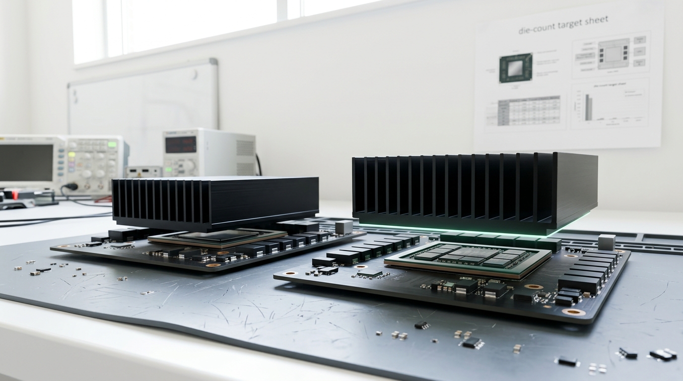
Every account of China’s AI-chip ecosystem eventually cites a version of the same comparison: Huawei’s Ascend chips versus Nvidia’s, measured in raw performance. That comparison is real and worth having, but it is not the sharpest available lens, and it is not the one that best explains why the gap persists. The sharper lens is yield — the fraction of manufactured chips that actually work well enough to sell — and on that measure, the reported numbers are stark.
The number
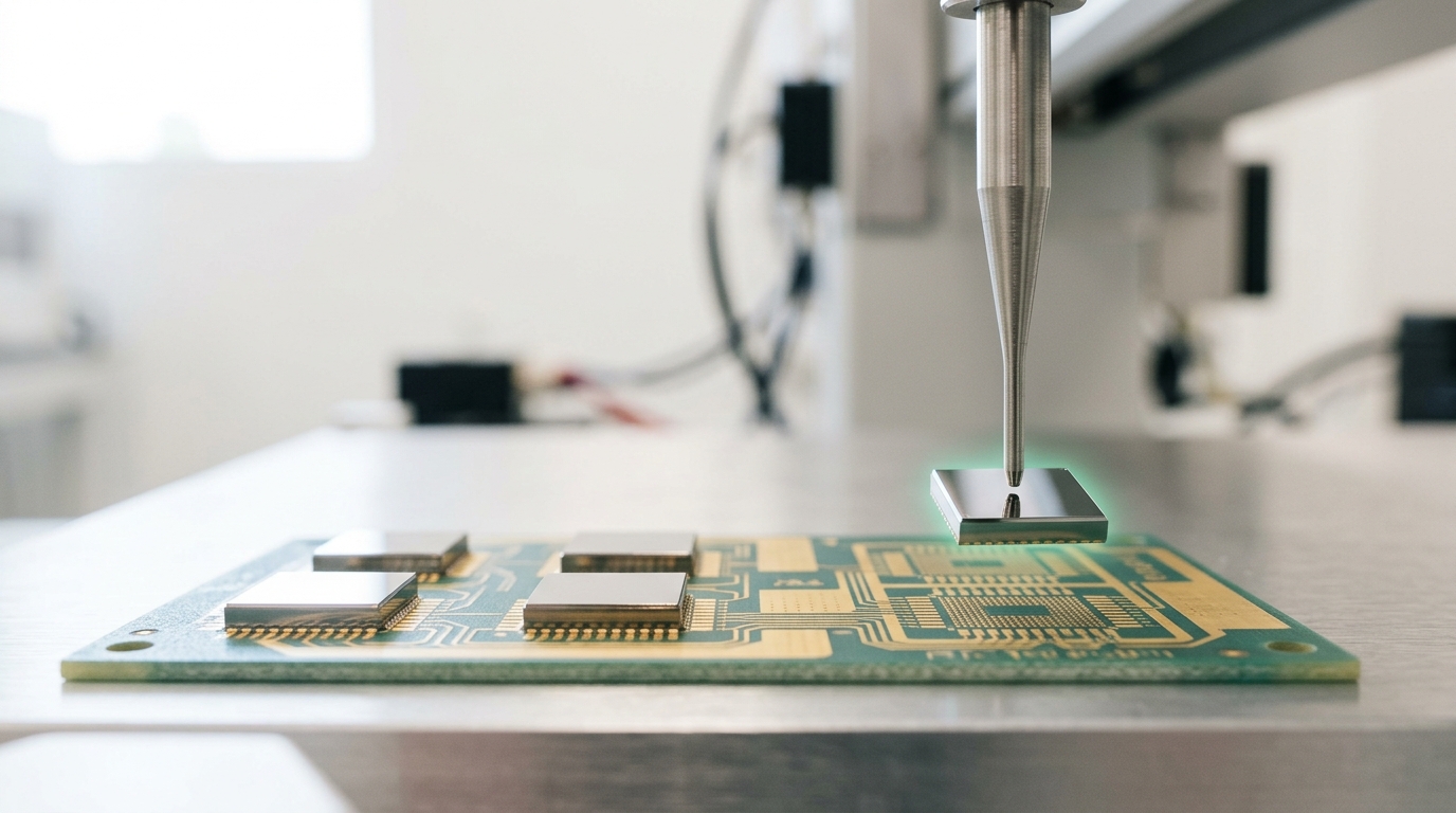
Huawei’s Ascend 910C, the company’s best currently shipping AI chip, is manufactured on SMIC’s domestic process. Reported yield on the 910C sits at 20-40%, far below the yields TSMC and Samsung routinely achieve on comparable-complexity leading-edge parts [1]. A yield in that range means that for every chip that ships, one to four more were manufactured and discarded — each one having consumed the same wafer area, the same lithography time, and the same scarce fab capacity as the chip that worked.
Why yield, not clock speed, is the right comparison
A performance-gap number — “chip A is five times faster than chip B” — describes the best unit each side can produce. A yield number describes what it costs, in wasted capacity, to get there at all. Low yield does not just raise the price of each working chip; it caps the total volume a fab can produce in a given period, because defective die still occupy wafer area and processing time that could have gone to a working one. SMIC’s own strategic response — mass-producing the Ascend 910B alongside a planned doubling of 7nm capacity in 2026 [2] — is best read as compensating for low yield with sheer additional capacity, rather than as evidence the yield problem has been solved.
Why SMIC is stuck at 7nm in the first place
SMIC’s process ceiling is not a talent or capital problem in the way it is sometimes framed. It is a direct consequence of export controls on EUV lithography tools, which are not available to Chinese fabs [1]. Without EUV, SMIC and its domestic peers rely on deep- ultraviolet (DUV) tools pushed through multiple patterning passes — exposing and etching a wafer several times to approximate features a single EUV exposure would print directly. This is a real, functioning workaround, not a myth, and it is a large part of how SMIC’s near-frontier chips get made at all [4]. It is also inherently lower-throughput and more defect-prone than single-exposure EUV patterning, which is a direct, physical contributor to the 910C’s reported yield range.
| Factor | Effect on Ascend 910C economics |
|---|---|
| No EUV access | Forces multi-pass DUV patterning |
| Multi-pass patterning | Lower throughput, more defect opportunities |
| Reported yield, 20-40% | 1.5-5x more wafers needed per working chip than a well-yielding line |
| SMIC’s response | Capacity expansion (7nm doubling), not yield-first optimization |
The estimate worth treating with real caution
One widely cited estimate places China’s overall advanced-chip production capacity at roughly 1-2% of US capacity in 2026 [3]. That figure should be read as exactly what it is — one analysis’s estimate, built on assumptions about what counts as “advanced” and how yield and capacity are weighted together — rather than as a settled, precise fact. The yield mechanics traced in this briefing are the more durable, verifiable part of the story; the specific single-digit percentage comparing national capacities is the part most likely to be revised as more production data becomes public.
What would actually change the picture
Two developments, and only two, would meaningfully change this analysis rather than merely updating it at the margins. The first is EUV access: any relaxation of export controls that let SMIC acquire even a small number of EUV systems would be a bigger single change to China’s domestic-chip trajectory than any design or software improvement Huawei could make on its own, because it would attack the constraint at its actual source rather than working around it. The second is a genuine yield breakthrough on the existing DUV multi-patterning approach — evidence that SMIC has found a way to push reported yields well above the 20-40% range using process refinements alone, without new tooling. Absent either development, the multi-pass DUV workaround and its associated yield ceiling are likely to remain the defining physical constraint on how much competitive AI silicon China’s domestic supply chain can actually produce, regardless of how sophisticated any individual chip’s architecture becomes on paper.