The light is not a lamp
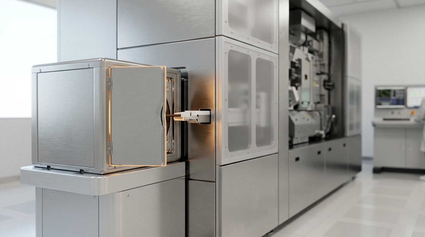
Extreme ultraviolet lithography is usually summarized by its output — a 13.5-nanometer beam — as though a scanner contained a specialized bulb. It does not. The light is the byproduct of deliberately destroying tens of thousands of droplets of molten tin every second, in a two-step sequence engineered so the resulting plasma emits in a narrow band around 13.5 nanometers rather than as a broad, useless glow. Everything downstream of that decision — the mirrors, the vacuum, the throughput arithmetic of a fab — follows from how that plasma is made and what it takes to keep the light it produces alive long enough to expose a wafer.
This article works through four mechanisms that a tour of a fab floor does not usually stop long enough to explain: how the light is actually generated inside the source, why the mirror that reflects it fixed the wavelength rather than the other way around, what physically happens as a modern transistor’s layers are built and rebuilt on top of a wafer, and how a fab’s control systems catch a process drifting out of specification before it turns into scrapped die. None of the four is a diagram-level abstraction. Each is a specific, checkable piece of physics or process engineering, and each is stranger, in its particulars, than the summary version usually presented.
Making the light: two strikes on the same droplet
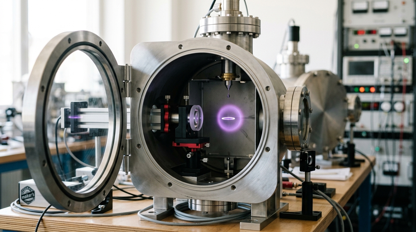
A laser-produced-plasma EUV source works on a target that is deliberately tiny and deliberately brief. ASML describes molten tin droplets around 25 microns across, ejected from a generator at 70 meters per second, at a rate of 50,000 droplets every second [2]. Independent review of the underlying physics puts the scale in the same range — mass-limited droplets on the order of 30 microns in diameter — chosen specifically because a small target minimizes debris while still holding enough mass to produce a usable plasma at high repetition rate [1].
Each droplet is not struck once. It is struck twice, by design. A first, low-energy laser pulse — delivered as a longer pulse lasting tens to around a hundred nanoseconds, or as a shorter, high-intensity pulse that triggers explosive cavitation — reshapes the falling sphere into a thin, flattened disc [1]. A second, far more powerful pulse then strikes that disc and vaporizes it into a plasma [2]. The reshaping step exists because a flattened target couples far more efficiently to the second pulse than a sphere does: more of the tin ends up in the plasma at the temperature and density that actually produce 13.5-nanometer light, and less is wasted as debris that would otherwise coat the collector mirror sitting behind it.
The plasma that results is genuinely extreme: electron temperatures in the range of 20 to 40 electron-volts, and electron densities that reach somewhere between 10^19 and 10^21 per cubic centimeter depending on the driving laser [1]. At those conditions tin is stripped to a narrow, specific band of charge states — ions carrying roughly eight to fourteen fewer electrons than neutral tin — and it is transitions within that particular charge-state band, arising from the 4d electron shell, that happen to cluster into a dense, overlapping set of spectral lines, called an unresolved transition array, sitting almost exactly at 13.5 nanometers [1]. Tin was not chosen because it is convenient to handle. It was chosen because, among the elements considered, this specific charge-state physics happens to land its emission where the mirrors described below can reflect it.
Even with the target and the charge states right, most of the input laser energy does not become EUV light. Current industrial sources are described as achieving conversion efficiency surpassing 5.5 percent, with output powers beyond 250 watts at intermediate focus, against a theoretical ceiling estimated near 9 percent [1]. That is the plasma-physics floor under a number that shows up constantly in industry discussion of EUV scanner throughput: source power is not a manufacturing-engineering shortfall to be fixed with a bigger laser. It is bounded by how efficiently a pulse of laser energy can be converted into tin ions sitting in exactly the right charge states, and that efficiency has a ceiling set by atomic physics rather than by capital spending.
The mirror that decided the wavelength
None of that light does any good without something to reflect it, and reflecting 13.5-nanometer light turns out to be its own separate, equally strange problem. ASML states plainly that most materials absorb extreme ultraviolet light, which is why the projection system uses no lenses at all — everything that shapes and focuses the beam is a mirror [3].
A single reflective surface will not do it. The mirrors used in EUV systems are not a polished metal surface but a stack of dozens of alternating molybdenum and silicon layers, each only a few atomic layers thick, engineered so that the many weak partial reflections at each interface add together in phase. A close analogue to the classical Bragg condition for layered reflectors,
describes why the stack works at all: at near-normal incidence,
ASML’s own description of the finished mirrors is that each one carries over 100 individually engineered layers and is polished to a smoothness under one atom’s thickness — illustrated with the comparison that if a mirror were scaled to the size of Germany, its tallest imperfection would be about a millimeter high [3]. That degree of control matters because the interface quality measured above — roughness below 0.2 nanometers, interdiffusion held to a few tenths of a nanometer — is what stands between a stack that reflects roughly two-thirds of the light landing on it and one that reflects far less, since interdiffusion between molybdenum and silicon layers degrades the sharp boundaries the interference effect depends on.
Absorption is also why the entire beam path, not just the optics, has to run in vacuum. EUV light is absorbed by essentially everything it passes through, air and nitrogen included, so there is no atmosphere the beam can be allowed to cross between the source and the wafer [5]. That creates an odd secondary problem: the plasma that makes the light also throws tin debris onto the collector mirror sitting closest to it, and pumping the chamber to a hard vacuum does nothing to stop that. The industry’s answer is to deliberately reintroduce a small amount of a specific gas — hydrogen — around the collector, at low pressure, because hydrogen reacts with deposited tin to form stannane, a volatile tin hydride that a vacuum pump can then remove before it builds into an opaque film [5]. Hydrogen is difficult to pump precisely because the molecule is so small, which makes the buffer-gas system a genuine engineering trade rather than an incidental detail: the industry accepts a harder pumping problem in exchange for a mirror that survives being sprayed with metal vapor fifty thousand times a second.
Building one transistor, layer by layer
Step back from the light source and look at what it is actually printing onto. A modern logic transistor is not deposited in one pass. It is assembled from a sequence of distinct material layers, several of which are put down, shaped, and then deliberately removed and replaced before the device is finished.
The clearest public illustration of why a layer gets replaced rather than built once is Intel’s 2007 disclosure of its 45-nanometer process, the first high-volume logic technology to use a high-k gate dielectric in place of the silicon dioxide that had served since the 1960s. Hafnium oxide was reported to carry a dielectric constant near 25, roughly six times that of silicon dioxide [9], which lets the gate control the channel electrostatically through a physically thicker, more manufacturable film instead of a silicon-dioxide layer so thin it leaks current by quantum tunneling. But polysilicon, the gate material used for four decades, does not sit well on hafnium oxide, so the process used two different metal materials for the gate instead — one tuned for the PMOS transistor, one for the NMOS transistor [9]. That single substitution is the seed of what is now the industry-standard replacement-gate flow: a placeholder gate is patterned and then, once the transistor’s other layers have survived their high-temperature processing, is deliberately removed and replaced with the real high-k and metal-gate stack that would not tolerate that heat. Modern gate-all-around processes still describe this step by name — replacement metal gate, or RMG — and still treat it as one of the layers whose thickness is being actively scaled down, because reducing the vertical space the metal-gate stack occupies is what lets more stacked channels fit in the same footprint [6].

Around that gate module, the rest of the transistor is built from layers with correspondingly specific jobs: shallow trenches etched and refilled with oxide to electrically isolate one device from its neighbor; source and drain regions grown, not just implanted, so that a material with a different natural lattice spacing — silicon-germanium for the P-type transistor, for example — can mechanically strain the channel between them and change how fast carriers move through it; thin spacer layers that keep the gate from short-circuiting to the source and drain; a silicide layer where the wiring will actually make contact; and only then, above all of that, dozens of layers of copper interconnect separated by low-dielectric-constant insulators to wire the finished devices together. Each of those layers is itself a full pass through deposition, patterning, and etch. None of them is optional, and getting any one of them wrong does not usually make the transistor fail outright — it makes it slower, leakier, or more variable than its neighbors, which is a harder failure to catch than an open circuit.
From fin to sheet: why the channel’s shape had to change
By the time a transistor’s channel had shrunk to a few tens of nanometers long, a planar gate sitting on top of the channel could no longer hold electrostatic control over it: the source and drain, which are supposed to be controlled by the gate, start to influence the channel directly through the substrate underneath, a leakage effect that worsens as the channel shortens. The industry’s first fix was the FinFET, which stands the channel up as a thin vertical fin and wraps the gate around three of its four sides instead of one. Gate-all-around designs, and specifically the horizontally stacked nanosheet architecture that has now replaced FinFETs at the leading edge, wrap the gate around all four.
The reason that fourth side matters can be written down directly. A transistor’s subthreshold swing — how many millivolts of gate voltage it takes to change the drain current by a factor of ten — is well approximated by
where
Making that shape is itself a materials-science problem, not a lithography one. A nanosheet stack starts as an epitaxially grown superlattice — alternating layers of silicon and silicon-germanium grown directly on top of each other with no interruption in the crystal — which is then patterned into a fin-like structure. The silicon-germanium layers are sacrificial: after the dummy gate is removed, a highly selective etch dissolves the silicon-germanium away from between the silicon sheets while leaving the silicon itself essentially untouched, physically releasing each sheet so the gate stack can later be deposited on all four of its sides [6]. That etch has to be selective enough to leave few germanium residues behind and controlled precisely enough that the released, unsupported sheets do not stick together or sag under their own weight during the release [6].
The step described as the single most complex module in the whole flow is what fills the gap the etch just opened. An inner spacer — a thin dielectric plug — has to be built into exactly the cavity left where the silicon-germanium used to connect the channel to the source and drain, isolating the future metal gate from the source and drain regions without blocking the channel itself, and it has to do this with high etch selectivity and precise lateral control on a feature now suspended in air on both sides [6]. Get the inner spacer’s lateral dimension wrong and the transistor either leaks through parasitic capacitance or fails to make proper contact — and unlike a via landing off-target, this is not a placement error the scanner can be blamed for; it is a materials and etch-chemistry outcome set entirely inside the nanosheet module.
Work function metal — the layer that sets each transistor’s threshold voltage by tuning the effective work function seen by the channel — has to be deposited into that same released, four-sided gap, and its own thickness has become a scaling variable in its own right. Reducing the vertical spacing the work function metal stack needs between sheets from about 13 nanometers to about 7 nanometers is reported to deliver roughly a 10 percent improvement in AC circuit performance on its own, independent of any change to the channel [6]. An industry alliance’s own account of the earliest version of this architecture — demonstrated jointly and presented at the 2017 VLSI Technology and Circuits conference in Kyoto — claimed that a nanosheet-based technology could deliver 40 percent higher performance at fixed power, or 75 percent lower power at matched performance, relative to the leading-edge 10-nanometer technology then on the market [7]. That is a claim from the companies that built the demonstration device, made about their own technology, not an independently measured production result, and it should be read as exactly that: a target the architecture was built to hit, stated by the parties with the clearest interest in it looking good.
The loop that watches the loop
None of the preceding sections describes a process that runs the same way twice. Every deposition, etch, and exposure varies slightly, tool to tool and wafer to wafer, and the entire discipline of process control exists to catch that variation drifting toward a limit before it produces a bad die rather than after.
The oldest tool for doing this is the control chart, and it works by testing a sequence of measurements against known patterns rather than against a single pass/fail threshold. The classic Western Electric decision rules flag a process as suspect if, for example, a single point lands more than three standard deviations from the target, or two of three consecutive points land beyond two standard deviations, or a long run of consecutive points falls on the same side of the target line — patterns that are each individually unlikely under normal random variation and therefore signal that something about the process, not the sample, has changed [10]. Alongside the chart sits a single summary number, the process capability index,
comparing the distance from the process mean
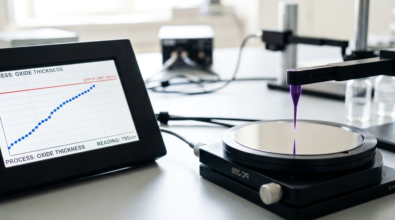
A control chart, on its own, only tells someone that a process has drifted. Advanced process control adds the mechanism that acts on it. Run-to-run control is described as a form of discrete control in which a tool’s recipe — not its hardware, its recipe — is adjusted between production runs specifically to minimize drift, shift, and variability before the next run inherits it; a chemical-mechanical-polishing tool, for instance, can have its per-wafer process time adjusted ahead of each run so that the amount of material actually removed tracks a target more tightly than the raw process ever would on its own [11]. Sitting alongside run-to-run control, fault detection and classification watches large volumes of tool and wafer sensor data in real time, compares it against learned thresholds, and flags equipment-level problems — not just excursions in the measured product — early enough to prevent scrap and unplanned downtime rather than merely explaining it afterward [11]. One industry account of these systems cites a SEMATECH study estimating that run-to-run control alone was worth more than $300 million a year to a 20,000-wafer-starts-per-month logic fab, through some combination of tightened specifications, reduced rework, and less unplanned downtime [11]. That figure is a vendor-adjacent industry estimate rather than an audited public result, and it should be read with that caveat attached — but the mechanism behind it is not in dispute: a fab that only measures after the fact pays for every excursion in scrapped wafers, while a fab that adjusts the next run’s recipe based on the last run’s measurement pays only for the correction.
The newest layer on top of this loop tries to remove metrology’s own delay from the equation. Virtual metrology predicts what a direct physical measurement would show — a deposited film’s thickness, for instance — from the sensor and process data already being collected as the tool runs, rather than waiting for a wafer to reach a separate measurement station [12]. A 2026 study describes a graph-attention model built specifically to correlate multiple simultaneous sensor streams during film deposition and predict the resulting measurement well enough to flag a process beginning to drift before the physical measurement would otherwise have been available at all [12]. The appeal is obvious: physical metrology is slow and destructive of throughput by definition, since the wafer has to sit still and be measured instead of moving to the next process step, so a prediction that is good enough to act on buys back time in a loop that has always been rate-limited by how fast a fab could confirm what it had actually built.
Predictions, with the observations that would falsify them
These are forecasts, separated from the sourced analysis above. Horizon: 15 August 2030.
One. Multilayer mirror reflectivity in production EUV systems will not move meaningfully past the high-60s to low-70s percent range achieved in laboratory samples today, because the physics bounding interface diffusion and roughness at these thicknesses is close to its practical limit rather than an engineering backlog. Disconfirmed if a manufacturer or national laboratory publicly reports a production-representative Mo/Si, or equivalent, multilayer mirror exceeding roughly 75 percent reflectivity at 13.5 nanometers under near-normal incidence.
Two. The inner-spacer and work-function-metal modules, not the lithography step, will remain the most frequently cited yield-limiting steps in gate-all-around processes through this window, because the physical release and fill of a suspended, four-sided nanosheet gap has less design margin than a supported, three-sided fin. Disconfirmed if leading-edge foundries publicly attribute the majority of gate-all-around yield loss to patterning or overlay rather than to the channel-release, inner-spacer, or metal-gate fill modules.
Three. Virtual metrology will expand from film-thickness prediction into a standard input for run-to-run recipe adjustment at more process modules, rather than remaining a research demonstration, because the throughput cost of physical metrology does not fall while wafer volumes and process-step counts keep rising. Disconfirmed if published fab process-control architectures in this window still route the large majority of run-to-run adjustments through direct physical measurement rather than model-predicted values.
What to take away
Four mechanisms, one thread through all of them: nothing about a modern chip is built once and left alone. The light that patterns it is made by striking the same droplet twice on purpose. The mirror that reflects it works only because dozens of near-atomic layers are engineered to add in phase, in a vacuum maintained partly by reintroducing a gas whose entire job is to carry away the metal the source itself deposits. The gate that switches the finished transistor is put down as a placeholder specifically so it can be torn out and replaced later, once the layers around it have survived the heat that would have destroyed the real thing. And the channel that gate wraps around is a shape left behind after a sacrificial layer is deliberately dissolved out from between two others, in a gap now filled by a spacer with less room for error than almost anything else on the wafer. None of that would stay in specification without a separate, continuously running loop that watches for drift and corrects the next run before the drift becomes a defect. The physics is not a metaphor for the manufacturing discipline that surrounds it; the manufacturing discipline exists because the physics leaves so little room for error.