Six transitions, each with a date attached
Popular accounts of chip manufacturing tend to flatten seventy years of specific, contested, expensively won engineering decisions into a single smooth curve labelled “Moore’s Law.” This article does the opposite. It reconstructs six discrete transitions in semiconductor fabrication — each with a named person, a specific date, and a document that can still be read today — and treats the smooth curve as the thing that needs explaining, not the starting assumption.
The six are: the planar process that made a transistor’s junction reproducible in 1959; Gordon Moore’s 1965 paper and the revision he made to it a decade later; the replacement of aluminum with copper interconnects, announced by IBM in 1997; the accidental rediscovery of immersion optics that rescued 193-nanometer lithography after 2001; the extreme ultraviolet program that ran from 1980s optics research through a 1997 industry consortium to production tools in the 2010s; and the High-NA EUV systems now shipping into fabs. None of these happened smoothly, and none of them was inevitable in the way the retrospective story makes them sound. Every date and figure below is attributed to the specific source that documents it.
A flat surface for an unreliable device
Before 1959, a transistor’s most sensitive feature — the p-n junction where its electrical behavior is actually decided — sat exposed at the edge of the device, wherever the mesa-etching process happened to leave it. Contamination and mechanical damage at that exposed edge were a leading cause of unreliability in early transistors.
Jean Hoerni, at Fairchild Semiconductor, had recorded an idea in December 1957 for a different approach: leave the protective oxide layer used during diffusion in place over the junction, rather than etching it away, so the junction stayed permanently sealed under glass rather than exposed at a cut edge. He wrote up a patent disclosure in January 1959 and had a working planar transistor by March of that year [4]. The patent itself, “Method of Manufacturing Semiconductor Devices,” was filed on May 1, 1959, names Hoerni as sole inventor, and lists Fairchild Camera and Instrument Corporation as assignee; it issued on March 20, 1962 [3]. Fairchild moved the process into commercial production with the 2N1613 transistor in April 1960 and then licensed the rights across the industry [4].
The word “planar” describes the geometric consequence, and it is easy to undersell how much followed from it. A transistor whose junction is sealed under an unbroken, flat oxide layer can have that oxide selectively opened with photolithography to define exactly where a metal contact lands, on a surface that stays flat from one processing step to the next. Every later technique this article covers — patterning smaller features, adding more wiring levels, stacking more layers — depends on that flatness being preserved layer after layer. The planar process did not just fix a reliability problem; it created the flat, photolithographically addressable surface that made an integrated circuit, built up in successive patterned layers on one piece of silicon, a manufacturable object rather than a laboratory curiosity.
The paper that predicted, then corrected, its own curve
Six years later, Gordon Moore — by then Director of Research and Development Laboratories at Fairchild Semiconductor — published a four-page article titled “Cramming More Components onto Integrated Circuits” in the trade magazine Electronics, Volume 38, Number 8, dated April 19, 1965 [1]. The paper’s argument was economic before it was technical: as more components are integrated onto a single chip, the cost per component falls, and that falling cost is itself what drives designers to integrate still more. Moore’s now-famous extrapolation from that argument was that the number of components per chip would reach 65,000 by 1975, implied by a doubling roughly every twelve months from the handful of components on the integrated circuits of the early 1960s [2].
It is worth being precise about what that claim was and was not. It was not a physical law, and Moore did not call it one — the name “Moore’s Law” was coined later, by others. It was a single engineer’s extrapolation of a short observed trend, published in a trade magazine rather than a peer-reviewed journal, covering roughly ten years. Ten years after publication, at the 1975 IEEE International Electron Devices Meeting, Moore revisited the projection with a decade of real data and revised the rate downward: from a doubling every twelve months to a doubling every two years. He attributed the original decade’s pace to advances in photolithography, wafer size, process technology, and what he called “circuit and device cleverness,” and noted that the newer microprocessor designs of the mid-1970s were somewhat less dense than the memory chips that had driven the earlier rate [2].
The two numbers are worth writing down side by side, because the difference between them is itself a historical fact rather than a rounding error. If
with
When aluminum ran out of road
For roughly three decades after the planar process, aluminum was the industry’s default interconnect metal: it adheres well to silicon dioxide, it is straightforward to deposit by evaporation or sputtering, and it can be patterned by plasma etching. That third property — the ability to convert the metal into a volatile compound a plasma can carry away — turned out to be a property copper does not share, which is part of why the eventual switch required a new process, not just a new material.
The problem with aluminum was forecast well before it was solved. Engineers had projected, as early as the mid-to-late 1980s, that as wire widths continued to shrink, aluminum’s resistance would rise to the point of dominating circuit delay, and that the accompanying rise in current density would accelerate electromigration — the gradual displacement of metal atoms by the “electron wind” of the current itself, eventually opening voids in a wire and failing the circuit [5]. IBM’s own account describes the combination of rising resistance and rising capacitive coupling between closely packed lines as “a two-headed monster” facing the industry’s device planners [5].

Copper solves the resistance half of that problem directly — it is a noticeably better conductor than aluminum — but it cannot be deposited and plasma-etched the way aluminum was, and it diffuses readily into silicon and its oxide, poisoning devices if left uncontained. IBM’s route to a working copper process came from an unrelated part of the company: engineers who had been developing copper electrochemistry for advanced packaging recognized electroplating, not the chemical- or physical-vapor deposition methods other groups were pursuing, as the practical way to fill fine copper wiring, with a diffusion barrier layer isolating the copper from the surrounding silicon dioxide [5]. On September 22, 1997, IBM announced it had manufactured working chips using this copper interconnect process — a “press release heard around the world,” as the account of the announcement later put it — and described the moment as the successful end point of a decade-long search for a material to replace aluminum. IBM stated it would ramp copper production over the following three quarters on its 220-nanometer microprocessor line [5]. Within a few years, copper interconnect was standard practice across the leading-edge industry, not an IBM-specific technique.

Adding a layer of water
By the early 2000s, the industry’s wavelength roadmap had a gap in it. The step planned after 193-nanometer deep-ultraviolet lithography was 157-nanometer lithography, using lenses made of calcium fluoride — and by 2002, delays and technical problems with that path had become severe enough to draw the industry’s direct attention to alternatives [6].
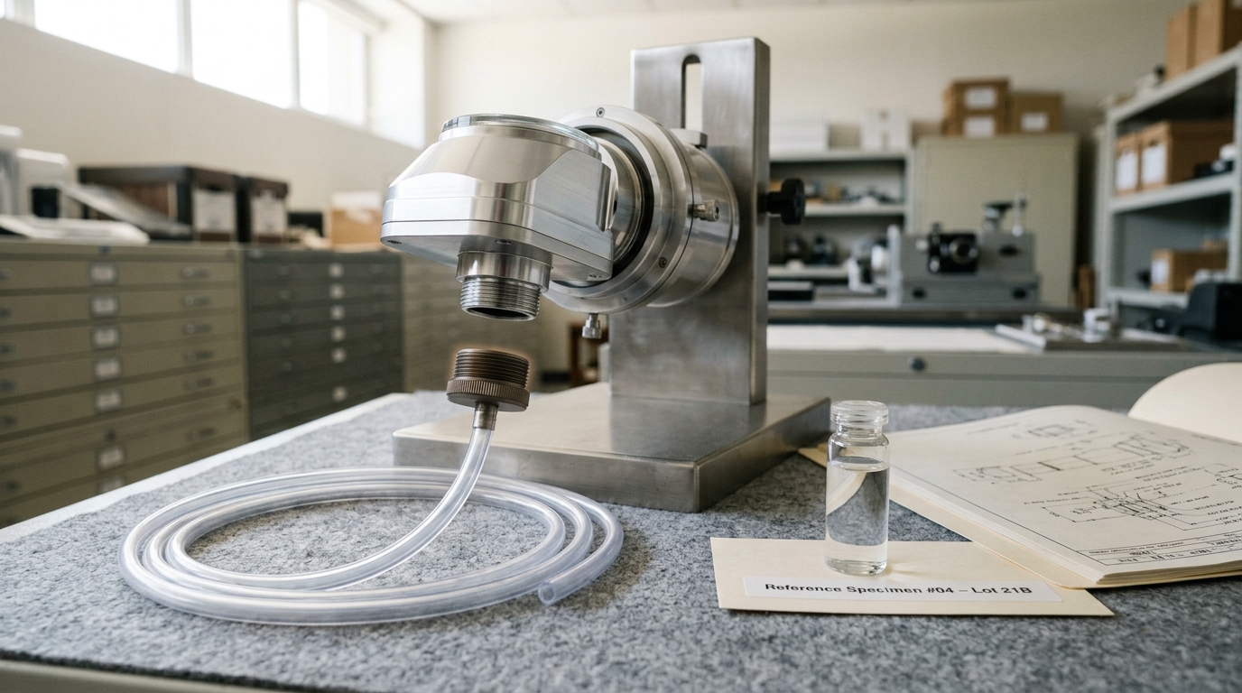
The alternative that emerged was, in its essence, a nineteenth-century idea. Immersion had been used to increase the resolving power of optical microscopes since the 1880s, and its application to modern lithography had been suggested, without being pursued, as early as the 1980s [6]. It resurfaced in December 2001, when ASML researcher Jan Mulkens attended an industry conference on 157-nanometer lithography and came away with the idea of putting a layer of purified water between the final lens and the wafer to sharpen the image the existing 193-nanometer scanners could produce, rather than pushing ahead to a shorter, harder wavelength [7]. Detlef Lohse, a professor at the University of Twente, worked out the fluid dynamics of maintaining a stable water layer under a scanning lens, while ASML senior vice president Jos Benschop oversaw the engineering that turned the idea into hardware [7].
The industry moved quickly once the idea had a name. SEMATECH organized an immersion workshop in July 2003 at which scanner suppliers presented development plans for “193i” immersion tools, prompting SEMATECH and its member companies to redirect development resources away from 157-nanometer lithography [6]. The first full-field 193-nanometer immersion scanner — an ASML AT1150i alpha tool, with a 0.75 numerical aperture — was delivered to the Albany Nanotech research facility in August 2004 [6]. By the end of that same year, TSMC had announced the first fully functional 90-nanometer-node chips manufactured on early immersion systems [7]. Adoption then scaled fast by the standards of lithography tooling: through December 2006, more than thirty 193-nanometer immersion scanners had been sold to chipmakers worldwide [6]. Immersion lithography did not replace the existing 193-nanometer wavelength; it extended the useful life of the scanner generation the industry already had, buying roughly a decade before the next wavelength change actually arrived.
Thirty years from an optics bench to a production line
Extreme ultraviolet lithography’s history is the longest and most expensive of the six, and it is worth tracing from its genuinely early research roots rather than from its production debut, because the gap between the two is itself the point.
The earliest projected EUV images were produced in the mid-1980s in Japan by Hiroo Kinoshita, building on multilayer-mirror research done in Russia during the 1970s; a separate group in the Netherlands, led by Fred Bijkerk, projected its own first EUV images in 1990 [8]. On the funding side, the U.S. Defense Advanced Research Projects Agency began supporting lithography research in 1991, the same period in which Nikon and Hitachi in Japan started their own EUV research programs, and Intel committed roughly two hundred million dollars to EUV development in 1992 [9].
Government funding proved unstable. When Congress terminated Department of Energy funding for the effort in 1996, Intel stepped in, and in 1997 Intel, together with AMD and Motorola, formed the EUV LLC consortium to fund EUV research at three U.S. national laboratories — Lawrence Berkeley, Lawrence Livermore, and Sandia — under a cooperative research and development agreement valued at roughly two hundred fifty million dollars, with Intel as the largest single funder [9, 11]. That work was formalized as a “Virtual National Laboratory” spanning the three sites, with a mandate to develop EUV lithography specifically for commercial chip manufacturing [11]. In 1997, ASML separately brought in Jos Benschop — the same engineer who would later drive immersion lithography into production — to start its own EUV program [8], and by 1999 ASML had secured licensing rights to the consortium’s work, becoming the only non-U.S. company admitted to it [9]. ASML strengthened its position in lithography tooling more broadly in 2001 by acquiring Silicon Valley Group, a U.S. toolmaker [9]. A separate European consortium, EUCLIDES, was formed in 1998 to pursue parallel EUV development [8].
A useful marker of how the effort was viewed at the time comes from an April 2001 Sandia news release announcing completion of the Engineering Test Stand, a prototype “alpha” EUV exposure tool built by the consortium, funded from 1997 through early 2002 by six semiconductor companies — Intel, Motorola, AMD, Micron Technology, Infineon, and IBM — working with the three national laboratories [10]. The release described the milestone as proof “that EUV lithography works,” and separately projected that EUV-built processors would reach speeds of up to 10 gigahertz by 2005 or 2006 [10]. That specific performance forecast is worth flagging precisely because it did not hold: EUV would not reach volume production for another twelve to eighteen years, and processor clock speeds in 2005–2006 were nowhere near 10 gigahertz. It is a useful reminder that a working prototype and an imminent product are different claims, and that even the consortium’s own scientists were, in this instance, wrong about the gap between them.

The EUV LLC program concluded in 2003, having met its technical goals [9]. ASML shipped its first prototype EUV lithography tools to the imec research consortium in Belgium and to the University at Albany’s SUNY nanotechnology center in 2006 [8, 9], and in 2008 the SUNY site used its demonstration tool to produce the world’s first full-field EUV test chips [8]. Industry attention kept building through the late 2000s: an LLNL article from June 2008 describes TSMC outlining an EUV-inclusive lithography roadmap at a technology symposium that April, and notes that LLNL had, over the program’s six principal years from 1997 to 2003, won seven R&D 100 awards for EUV-related work, with Intel researchers writing to praise the laboratory’s contributions as late as 2007 [11].
Commercial hardware followed on a slower schedule than the prototypes had suggested. ASML shipped the first TWINSCAN NXE:3100 — a pre-production EUV system — to a Samsung research facility in 2010, and shipped its first EUV production system, the TWINSCAN NXE:3300, in 2013 [8, 9]. Capital followed the same trajectory: in 2012, TSMC, Samsung, and Intel invested roughly one billion, one billion, and four billion dollars respectively into ASML, tied to accelerating EUV and next-generation lithography development [9]. The first EUV-enabled commercial product to reach consumers was Samsung’s Galaxy Note10, released in 2019 — a full thirty-four years after Kinoshita’s first projected EUV images and twenty-two years after the EUV LLC’s formation [8]. ASML shipped its hundredth EUV system in December 2020, and by the end of 2021 had 127 of its latest-generation EUV machines installed at customer sites [8].
The frontier the history has reached
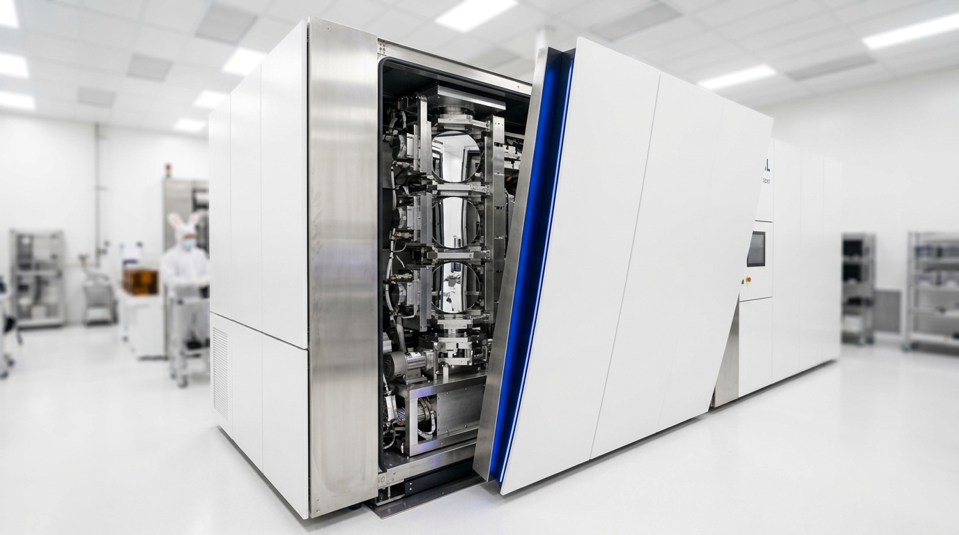
The arc does not stop at 2019. ASML shipped the first modules of its first High-NA EUV lithography system — the TWINSCAN EXE:5000, using a larger numerical aperture than the production EUV tools that preceded it — to Intel in December 2023, describing it as the outcome of roughly a decade of research and development [13]. ASML’s own account states that customers were expected to begin process research and development on the new tools through 2024 and 2025, moving into high-volume manufacturing in 2025–2026, with a stated roadmap toward raising system throughput to 220 wafers per hour in 2025 [13]. Those are the vendor’s own stated targets rather than independently audited production results, and they belong in the analysis as a claim, not a settled fact — but they are the most recent entry in a chain of dated entries that stretches back, without a gap, to Hoerni’s 1959 patent disclosure.
What the dates add up to
Read end to end, the six transitions share a structural feature that is easy to miss when each is told as an isolated technical anecdote: every one of them raised the capital, scientific, and organizational threshold required to stay on the leading edge, and none of them lowered it. The planar process turned transistor manufacture into something that could be licensed and industrialized; Moore’s paper turned continued miniaturization into a competitive expectation rather than an occasional achievement; the copper transition required an electrochemistry capability most chipmakers did not have in-house; immersion lithography and EUV each required the kind of coordinated, decade-plus, consortium-funded research program that only a handful of companies and national governments could sustain.
The resulting concentration shows up directly in industry statistics. A Congressional Research Service account found that at year-end 2015 there were 94 advanced semiconductor fabs in operation worldwide, of which 17 were in the United States, 71 in Asia — including 9 in China — and 6 in Europe; looking specifically at 300-millimeter wafer fabs, the geographic split was South Korea 26 percent, Taiwan 24 percent, Japan 18 percent, North America 13 percent, China 8 percent, Europe 3 percent, and the rest of the world accounting for the remainder [12]. The same account put the cost of a single state-of-the-art 300-millimeter fab at as much as ten billion dollars, and recorded that U.S. semiconductor firms’ domestic spending on new plants and equipment ranged from seventeen billion dollars in 2013 to about twenty-two billion dollars in 2011 [12]. Those numbers predate EUV’s move into volume production and High-NA’s arrival entirely; each of the two most recent transitions in this history has raised the entry price again, not lowered it.
None of this is a criticism of any single decision along the way. Each transition solved a real, well-documented problem — an exposed junction, a resistance and electromigration limit, a wavelength dead end, a mirror reflectivity too low to build a usable source around — using the best available approach at the time, verified in the sources cited throughout. But cumulatively, the history is one of rising thresholds rather than falling ones, and the industry’s current geography is close to what that pattern would predict rather than being a separate, unrelated fact about trade policy or geology.
A forward note, kept separate from the history
Everything above is a reconstruction of the past; the following is a forecast, marked as one. Horizon: the next four years, through 2030. Assumption: no lithographic modality outside EUV and High-NA EUV projection optics reaches high-volume manufacturing within that window, and no government intervention materially subsidizes a new entrant’s fab construction costs.
Forecast. The number of organizations capable of operating at the fabrication frontier will not increase from its current small set, and may fall further as High-NA deployment concentrates spending among the handful of customers who placed early orders. Observable indicator: the list of announced High-NA EUV customers remains limited to the same handful of companies that were already operating EUV production fabs before 2023. Disconfirmed if a chipmaker without a prior EUV production line brings a High-NA-based leading-edge process to volume manufacturing before 2030, or if a fifth country beyond the United States, South Korea, Taiwan, and the EU/Japan bloc hosts a High-NA-equipped fab by that date.
What to take away
Every widely repeated claim about how chip manufacturing “always” advances rests on a small number of specific, dated events: a patent disclosure written in January 1959, a four-page trade-magazine article from April 1965 that its own author revised in 1975, a press release from September 1997, a conference aside from December 2001, a consortium agreement from 1997 that took until 2019 to reach a consumer product, and a shipment to Intel in December 2023. None of these was smooth, several of the era’s own confident predictions about timing turned out to be wrong, and each transition made the next one more expensive rather than more accessible. The industry now visible from the outside — a small number of countries, a smaller number of companies, and fabrication tools that cost billions of dollars and take a decade or more to develop — is not a deviation from this history. It is what the history, read with its dates attached, was always going to produce.