Two disciplines, historically kept apart
Designing a chip’s electrical circuits and predicting how that chip will physically behave once built — how it dissipates heat, how it responds to mechanical stress, how its structure holds up under real operating conditions — have historically been separate engineering disciplines, served by separate software from separate companies. Synopsys’s acquisition of Ansys, a leading multiphysics simulation company, for roughly $35 billion, directly merges those two disciplines under one roof [2].

The deal’s long road to completion
Announced in January 2024, the acquisition required regulatory approval across the US, EU, UK, and China before closing — a genuinely global review reflecting how consequential regulators in each major jurisdiction judged the combination to be [4]. That multi- year, multi-jurisdiction process is itself informative: regulators do not subject a routine, low-impact acquisition to review across four separate major markets, and the scrutiny reflects how central both companies already were to their respective industries before the deal was even proposed.
Why “silicon-to-systems” is the right way to describe the combination
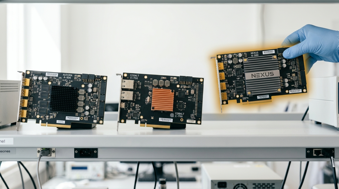
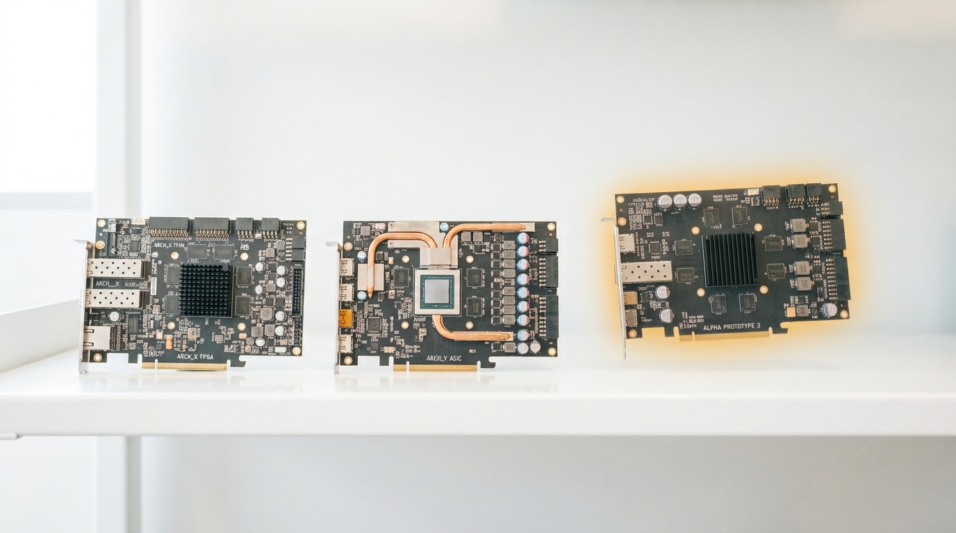
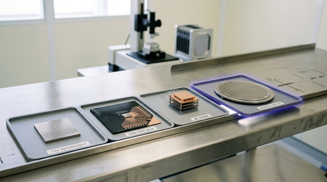
Coverage of the completed deal describes Synopsys’s resulting position as a “silicon-to- systems” powerhouse — spanning everything from a chip’s electronic design through to how that chip behaves as a physical object inside a larger system [1]. That framing matters directly for the AI hardware industry this cohort covers: a modern AI accelerator’s physical packaging, covered extensively in this cohort’s advanced-packaging and CoWoS briefings, increasingly determines its real-world performance as much as its circuit design does — thermal throttling, mechanical warpage across a multi-die package, and electromagnetic interference between densely packed components are all physics problems Ansys’s simulation tools address directly, previously requiring a separate toolchain from the circuit-design work Synopsys’s core EDA business already handled.
The first product of the combination
Roughly a year after the acquisition closed, Synopsys released its first Multiphysics Fusion tools, combining EDA and physics analysis technologies within a single design flow specifically targeted at advanced semiconductor systems [3]. That release timeline — meaningful integration taking a full year post-close — is a realistic reflection of how hard it actually is to merge two historically separate software platforms and engineering cultures into a genuinely unified workflow, rather than simply rebranding two still-separate tools under one corporate umbrella.
Why this matters beyond Synopsys’s own business
A chip designer who can simulate a package’s thermal and mechanical behavior within the same environment used to design its circuits, rather than exporting data between disconnected tools, can catch physical-design problems earlier and more cheaply in the development cycle — directly relevant to every company in this cohort racing to ship increasingly complex, densely packaged AI accelerators on tight competitive timelines. Whether Synopsys’s integrated approach becomes the new industry standard, forcing competitors like Cadence to pursue comparable combinations of their own, is one of the more consequential structural questions in the EDA industry heading into the rest of the decade.
Why physics simulation and agentic design are converging trends
This cohort’s companion briefing on Synopsys’s agentic AI design tools, announced at DAC 2026, and this acquisition are not separate stories — they are two halves of the same broader strategic direction. An autonomous design agent capable of proposing circuit changes benefits enormously from being able to immediately simulate that change’s physical consequences — thermal, mechanical, electromagnetic — within the same environment, rather than requiring a human engineer to manually export the design to a separate simulation tool and interpret the results before deciding whether to proceed. The Ansys acquisition, in other words, is infrastructure that makes Synopsys’s agentic-design ambitions meaningfully more powerful, not a separate business line pursued for its own sake.
What a competitor would need to do to respond
Cadence, Synopsys’s most direct competitor in core EDA tooling, faces a genuine strategic choice in response to this acquisition: pursue a comparable multiphysics acquisition of its own, build equivalent capability internally over a longer timeline, or attempt to compete on a narrower set of differentiated strengths instead of matching Synopsys’s combined breadth directly. Which path Cadence pursues, and how quickly, is one of the more consequential competitive questions in the EDA industry heading into the back half of the decade, with direct consequences for every chip designer, across every company covered in this cohort, that relies on one or the other vendor’s tools.