The claim this briefing is not making
This cohort’s companion briefing on Moore’s Law’s history argues the “law” was always a business plan, not a physical certainty — a framing consistent with how the observation is documented from its 1965 origin onward [8]. This briefing is not arguing Moore’s Law has already ended in 2026 — the current consensus among the sources reviewed here is more precise than that: scaling has shifted from traditional geometric transistor-density doubling to multidimensional performance improvement across energy efficiency, packaging, and system integration, rather than stopping outright [5]. What this briefing covers is the specific set of limits now close enough to matter, separating the ones already engineered around from the one that genuinely is not.
The problem GAA and backside power delivery actually solved
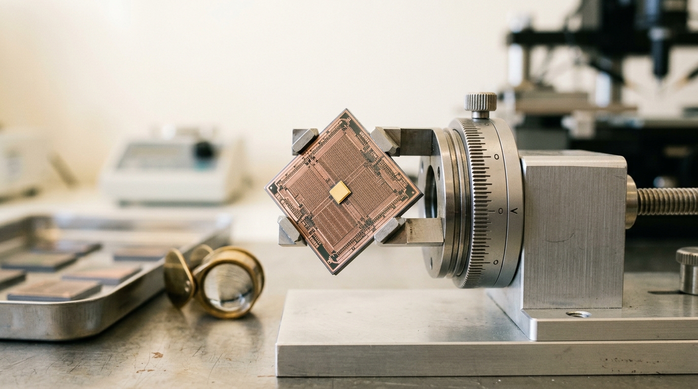
As gate length shrinks toward the size of a few silicon atoms, quantum tunneling takes over — electrons crossing barriers classical transistor design assumed they couldn’t, producing heat and leakage current that degrades performance [2]. The industry’s current-generation response is gate-all-around (GAA) transistor architecture, which wraps the gate fully around the channel rather than only alongside it, giving engineers substantially better control over current flow at atomic-scale dimensions — recent transport research on nanosheet GAA structures confirms the architecture measurably improves channel control at exactly the constriction points where tunneling risk is highest [7]. Paired with backside power delivery (BPD) — moving power-routing to the rear of the wafer instead of interleaving it with signal routing on the front — these two architectural moves are projected to extend viable transistor scaling for at least another decade [1]. TSMC’s own roadmap reflects this directly: A16, targeting H2 2026, is specifically built around backside power delivery [3], part of the same multi-fab N2-and-beyond ramp this cohort’s foundry-track coverage documents as running at an historically aggressive pace [9]. Peer-reviewed device literature on sub-5nm CMOS scaling reaches a compatible conclusion: continued scaling remains technically achievable through architectural innovation, at the cost of substantially increased process complexity per node [6].

The deeper problem these fixes don’t solve
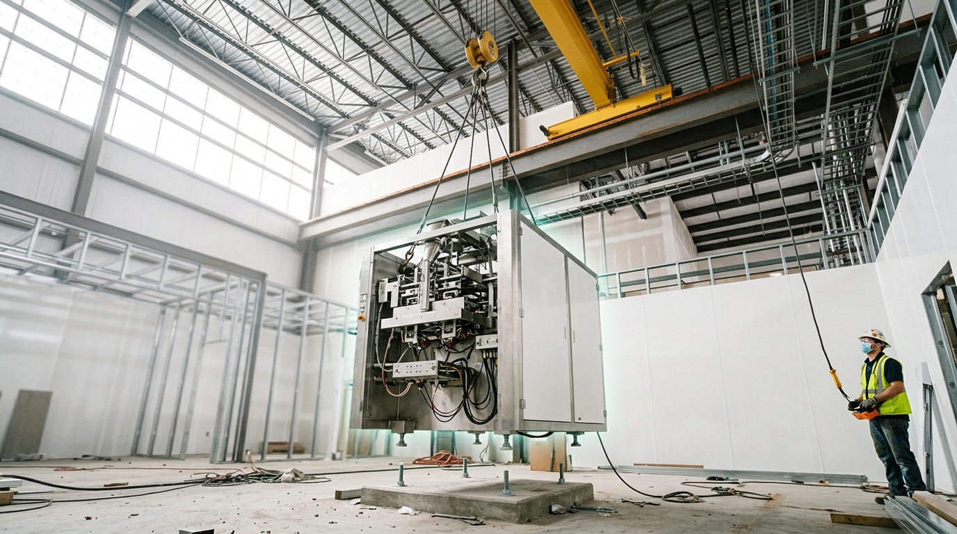
Underneath the quantum-tunneling and leakage problems GAA and BPD address sits a more structural issue: the end of Dennard scaling — the assumption, long since broken, that as transistors shrink, power density stays roughly constant. Once that assumption failed, shrinking a transistor stopped automatically delivering a proportional efficiency gain, meaning each new node has to work harder architecturally to deliver the performance improvement customers expect [1]. Layered on top of that physical problem is a straightforwardly economic one: below 5nm, fab construction and equipment costs now roughly double every two to three years, while transistor cost per unit rises and usable compute-per-watt gains plateau — meaning each new node demands substantially more capital for a shrinking marginal return [1]. TSMC’s own $265 billion total Arizona commitment, covered in this cohort’s foundry-track briefings, is one direct, dollar-denominated illustration of exactly this cost curve in action [4].
Why the economic limit is harder to engineer around than the physical one
Physical limits like quantum tunneling have historically yielded to architectural innovation — GAA is the latest in a long line of such fixes, following finFET before it and planar transistors before that. The cost-doubling problem is different in kind: it is not a specific physics problem with a specific architectural counter-move, but a compounding capital-intensity trend that makes each future node progressively more expensive to develop and manufacture regardless of which architecture eventually replaces GAA. This cohort’s equipment-track briefings on EUV and High-NA EUV lithography document exactly this dynamic from the supplier side: each successive lithography generation costs meaningfully more per tool than the last, and that cost gets passed through the entire supply chain this cohort covers.
What “ending Moore’s Law” would actually require
Taken together, the sourced picture is this: transistor-density scaling has not stopped, and GAA plus backside power delivery give the industry a credible path through at least the next decade of node transitions. What would actually end the multi-decade pattern Moore’s Law describes is not a single physics wall the industry hits and stops at, but the point where fab-cost doubling outpaces the revenue gains new nodes can generate — an economic ceiling, not a purely physical one, and one this briefing’s sources do not claim has been reached, or precisely dated, as of 2026.
Why this distinction matters for reading the rest of this cohort’s roadmap coverage
Every foundry-track briefing in this cohort discussing N2, A16, or beyond should be read against this specific distinction: the physical engineering problems have credible, funded solutions already in TSMC’s and Intel’s public roadmaps, while the economic sustainability of continuing to fund those solutions at a doubling cost cadence remains the genuinely open question — one this briefing does not resolve, because the sourced evidence available does not yet resolve it either.