How Edge AI Electronics and Sensor Systems Actually Work
Before a neural network ever sees a number, an analog front end has already decided what that number can mean. This is a mechanics walkthrough of the circuits, sensors and power budgets that make always-on inference possible in the field.
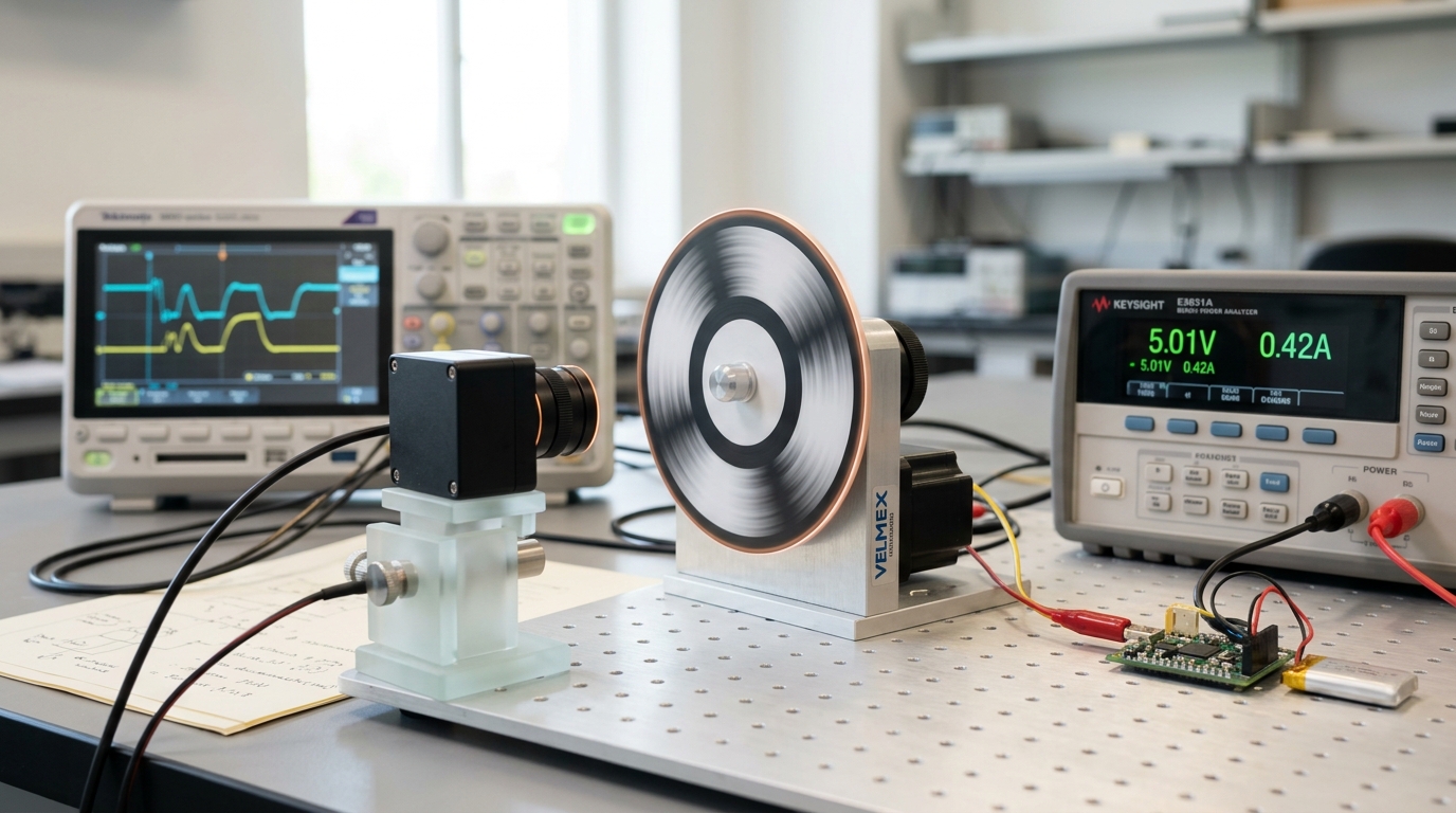
An edge sensor characterization bench: a calibration target mid-rotation in front of a bare event camera module, an oscilloscope and a bench power analyzer standing by. — Image prompt and art direction by Brecht Corbeel; generation pending.
Abstract
A deployed edge AI system is not a neural network with a camera attached to it; it is a chain of analog and mixed-signal decisions that happen before any inference runs at all. This article walks that chain in order: how an analog front end amplifies, filters and digitizes a raw sensor signal at a known noise floor; how an event camera's per-pixel asynchronous circuit differs mechanically from a frame sensor's global or rolling shutter; how a microcontroller-class NPU allocates a milliwatt-scale power budget across sensing, filtering and inference; and what actually breaks a field deployment that passed every bench test. Equations appear only where they expose a real constraint — quantization noise, event-rate bandwidth, and a power budget identity — not as decoration. Vendor claims, measured benchmark numbers and open questions are kept explicitly separate throughout.
A camera module, an inertial sensor, a microcontroller with a neural accelerator bolted onto it, and a battery: that is the parts list most people picture when they hear “edge AI.” It is also the wrong mental model, because it starts at the model and works outward. Almost everything that determines whether a field deployment works — the noise floor a system can actually resolve, the latency it can guarantee, the milliwatts it has left over for inference after sensing and communication take their share — is decided before a single weight is multiplied. This article walks the chain in the order the electrons actually take it: from a raw physical signal, through an analog front end that conditions it, into a digitizer that quantizes it, through a processor that budgets power across sensing and inference, and out into a field enclosure that has to survive temperature swings, vibration and years of unattended operation. Equations appear only where they expose a real constraint, not as decoration; vendor claims are flagged as claims; and the mechanics of an event camera are set against a conventional frame sensor because the difference is a genuine circuit-level distinction, not a marketing one.
The analog front end: deciding what the number can mean
Every embedded sensing chain begins with an analog front end (AFE) — the amplification, filtering and biasing circuitry that sits between a raw transducer and an analog-to-digital converter (ADC). This stage is easy to skip past in a systems discussion because it produces no discrete output of its own, but it is where most of a system’s achievable precision is actually decided. A microphone, a photodiode, an electrode or a strain gauge produces a signal that is simultaneously too small, too noisy and biased around the wrong voltage to hand directly to a digitizer. The AFE’s job is to apply a programmable gain, reject out-of-band noise and interference, and center the signal inside the ADC’s input range — all before a single bit has been recorded.
Texas Instruments’ ADS1298, an eight-channel front end built for biopotential measurement such as ECG and EEG, is a useful concrete example because its data sheet documents the whole chain explicitly: eight low-noise programmable-gain amplifiers feeding eight 24-bit delta-sigma ADCs, with an input multiplexer that can route internally generated test, temperature and lead-off-detection signals to each channel independently [5]. That lead-off detection is itself a small analog circuit whose entire purpose is to notice when the front end has lost a good electrical contact with its sensor — a reminder that “sensing” in a fielded system includes continuously checking whether the sensor is still sensing anything meaningful at all.
The delta-sigma architecture used in both the ADS1298 and Analog Devices’ AD7124-8 (an 8-channel, 24-bit low-power sigma-delta ADC aimed at industrial and instrumentation front ends) matters mechanically, not just as a spec-sheet number. A delta-sigma converter oversamples the input at a rate far above the signal bandwidth, then uses a noise-shaping loop to push quantization noise out of the frequency band of interest, where a digital filter can remove it. The AD7124-8’s data sheet documents this trade directly through its power-mode table: a low-power mode delivering 24 nV RMS noise at 1.17 samples per second and roughly 255 microamps, versus a full-power mode delivering 23 nV RMS at 9.4 samples per second and roughly 930 microamps [3]. Noise floor, sample rate and current draw are not three independent numbers a designer picks freely — they are three faces of one trade a delta-sigma converter is built around, and an edge-AI power budget inherits whichever point on that curve the front end is configured to.
The quantization step itself has a clean expression once gain and reference voltage are fixed. For an ADC with N effective bits resolving a full-scale reference voltage V_{ref}, the size of one quantization step is
q = \frac{V_{ref}}{2^{N}}
and, treating quantization error as uniformly distributed over one step, the resulting quantization noise power has a root-mean-square value of q / \sqrt{12}. This is the textbook derivation behind every “effective number of bits” figure a converter data sheet reports, and it is the reason oversampling helps: spreading the same quantization noise power across a wider sampled bandwidth before filtering it back down effectively lowers the in-band noise floor without changing the converter’s physical resolution. This is analysis grounded in a standard result, not a claim from either vendor’s marketing copy — both data sheets report measured effective noise in microvolts or nanovolts RMS directly, and those measured numbers are what a systems designer should budget against, not the nominal bit count printed on the package.
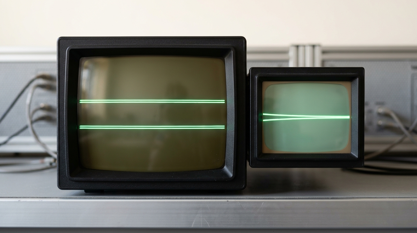
Figure 1. An analog front-end board mid-settle: the filtered channel has nearly reached its final reading while the raw probe point still shows noise. — Image prompt and art direction by Brecht Corbeel; generation pending.
Event cameras versus frame cameras: a different circuit, not just a different codec
The most mechanically distinct sensor in the edge-AI toolkit is the event camera, and the distinction is worth being precise about because it is frequently described loosely as “a camera that only sends changed pixels,” which understates what is actually different at the circuit level.
A conventional CMOS image sensor — global-shutter or rolling-shutter — exposes an entire array (or row-by-row slice of it) for a fixed integration time, then reads out every pixel’s accumulated charge on a synchronous clock, producing a full frame at a fixed rate whether or not anything in the scene changed. An event camera has no shared exposure clock at all. Each pixel contains its own photoreceptor and comparator circuit that continuously monitors the log of local light intensity and fires an asynchronous digital event — a timestamp, a pixel address and a polarity bit for brighter or darker — the instant that pixel’s local intensity crosses a threshold since its last event [1]. There is no frame boundary anywhere in this design; a pixel in total darkness with nothing moving in front of it can go seconds without producing a single event, while a pixel catching a fast edge can fire in microseconds. The survey by Gallego et al. reports the resulting properties directly from measured devices: temporal resolution on the order of microseconds, dynamic range figures around 140 dB compared with roughly 60 dB for a typical frame sensor, and substantially lower average power because pixels that see no change do no readout work at all [1].
The Sony/Prophesee IMX636, presented at ISSCC 2020, is a concrete instance of this circuit family and is useful for grounding the abstract description in real numbers. It is a stacked, back-illuminated 1280×720 sensor with 4.86-micron pixels, built with a per-pixel readout architecture supporting a reported 1.066 giga-events-per-second throughput, and it includes an on-chip programmable event-rate controller and a compressive data-formatting pipeline specifically to keep the output stream bounded when a scene suddenly becomes very active [2]. That event-rate controller is itself a small but important design admission: an event sensor’s raw output bandwidth is scene-dependent rather than fixed, so a real system built around one needs a circuit whose job is explicitly to cap and shape that bandwidth before it reaches the downstream bus, rather than assuming a constant frame-sized packet the way a conventional camera pipeline can.
This has a direct consequence for how an edge-AI power budget should be constructed. A frame camera’s power draw is close to constant regardless of scene content, because a full sensor read and a full frame’s worth of downstream processing happen on every tick. An event camera’s power draw tracks scene activity: a static scene with no motion produces close to no events and consequently close to no downstream processing load, while a busy scene produces a data-rate spike that a system’s processing pipeline — not just the sensor’s own rate controller — has to absorb. Building an always-on system around an event sensor therefore means budgeting for the worst-case event rate the rate controller is configured to allow, not the average case, because the average case is precisely the condition under which the sensor is cheapest and least interesting to design for.

Figure 2. A bare event-sensor die under inspection, one pixel row contacted by a probe needle mid-test while the rest of the array waits its turn. — Image prompt and art direction by Brecht Corbeel; generation pending.
Inertial sensing and the always-on interrupt pattern
Cameras are not the only sensor whose circuit design is built around minimizing when a processor has to wake up. Bosch Sensortec’s BMI270, an inertial measurement unit combining a 16-bit triaxial accelerometer and a 16-bit triaxial gyroscope in a package under 3 square millimeters, documents a current draw around 685 microamps in full always-on operation, and — more relevantly for a power budget — an internal power-management unit with motion-triggered interrupt logic that lets the host processor stay in a deep sleep state until the IMU itself decides an event worth reporting has occurred [4]. This is the same design principle as an event camera’s per-pixel comparator, applied to inertial sensing: push the decision of “has anything changed” as far down into dedicated low-power analog and mixed-signal circuitry as possible, so that the comparatively power-hungry general-purpose processor only has to wake up for events, not for polling.
This pattern — sensor-side wake logic feeding a normally-sleeping host — recurs across essentially every always-on edge-AI product category: voice assistants gating a full speech pipeline behind a low-power keyword detector, wearables gating motion classification behind an accelerometer interrupt, and industrial condition-monitoring nodes gating vibration analysis behind a threshold crossing on an accelerometer’s own comparator. The mechanism is identical in each case even though the physical sensor differs, and it is worth naming explicitly because it is the single largest lever available for meeting an always-on power budget: not a smaller model, not a more efficient matrix multiply, but a front-end circuit that keeps the expensive processor asleep most of the time.
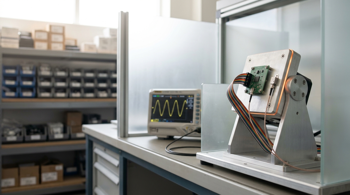
Figure 3. An IMU daughterboard mounted on a vibration shaker table, caught at the top of one stroke before the table reverses direction. — Image prompt and art direction by Brecht Corbeel; generation pending.
Budgeting power for on-device inference
Once a signal has been conditioned, digitized and gated by an appropriate wake mechanism, the question becomes what a microcontroller-class processor can actually afford to compute with the power that remains. A useful way to make this concrete rather than hand-wavy is a simple energy identity: the energy an inference actually costs is
E_{\text{inference}} = P_{\text{active}} \cdot t_{\text{active}}
and the sustainable average power of an always-on system operating at duty cycle d (the fraction of time spent active rather than in a low-power sleep state) is
P_{\text{avg}} = d \cdot P_{\text{active}} + (1-d) \cdot P_{\text{sleep}}
This identity is trivial algebraically, but it is exactly the trade a systems designer is making when choosing between “a bigger, slower model that runs less often” and “a smaller, faster model that still meets the same detection latency.” Neither P_{\text{active}} nor t_{\text{active}} is fixed by the model architecture alone; both depend on the accelerator the model runs on.
Arm’s Ethos-U55, a microNPU intended to sit alongside a Cortex-M-class processor rather than replace it, is documented by Arm as targeting up to a 480-times uplift in machine-learning inference throughput compared with running the same 8-bit and 16-bit quantized network purely on the companion CPU, in roughly 0.1 square millimeters of silicon area [7]. That is a vendor-reported architecture-level figure, not an independently measured benchmark result, and it should be read as such — a hardware-level uplift claim for the accelerator relative to running the identical workload without it, not a universal multiplier that applies to every model or every comparison a reader might construct from it.
For an independently measured cross-vendor picture of what different microcontroller-class systems actually achieve, MLPerf Tiny is the relevant reference. It is an industry-benchmark suite, developed collaboratively across more than fifty organizations, built specifically to measure accuracy, latency and energy together for devices in the 10–250 MHz range performing inference at under roughly 50 milliwatts, across four representative always-on tasks: keyword spotting, visual wake words, low-resolution image classification and anomaly detection from sensor data [6]. The benchmark’s own documentation is candid about how hard the energy measurement itself is to standardize — vendors differ in whether their reported numbers include peripheral power, firmware start-up energy or I/O activity — which is a genuinely useful caution: a published “X milliwatts” figure for an edge-AI part is only comparable to another vendor’s figure if both measured the same boundary around the system, and MLPerf Tiny exists in large part because that boundary was not being drawn consistently before it.
Put together, a realistic power budget for an always-on edge-AI node is not one number but an allocation across four consumers: the sensor and its analog front end in continuous low-power sensing mode, the wake-logic interrupt path, the burst of active compute when inference actually runs, and whatever radio or storage the system uses to report a result. The AFE and IMU numbers above are each individually modest — hundreds of microamps — but a system with several always-on sensing channels, each contributing its own baseline draw, can spend most of an average power budget before the neural network’s own energy is even counted. This is a common source of surprised field results: a model that benchmarks efficiently in isolation on a bench power supply still overruns a battery budget once every sensor channel that keeps it fed is switched on simultaneously.
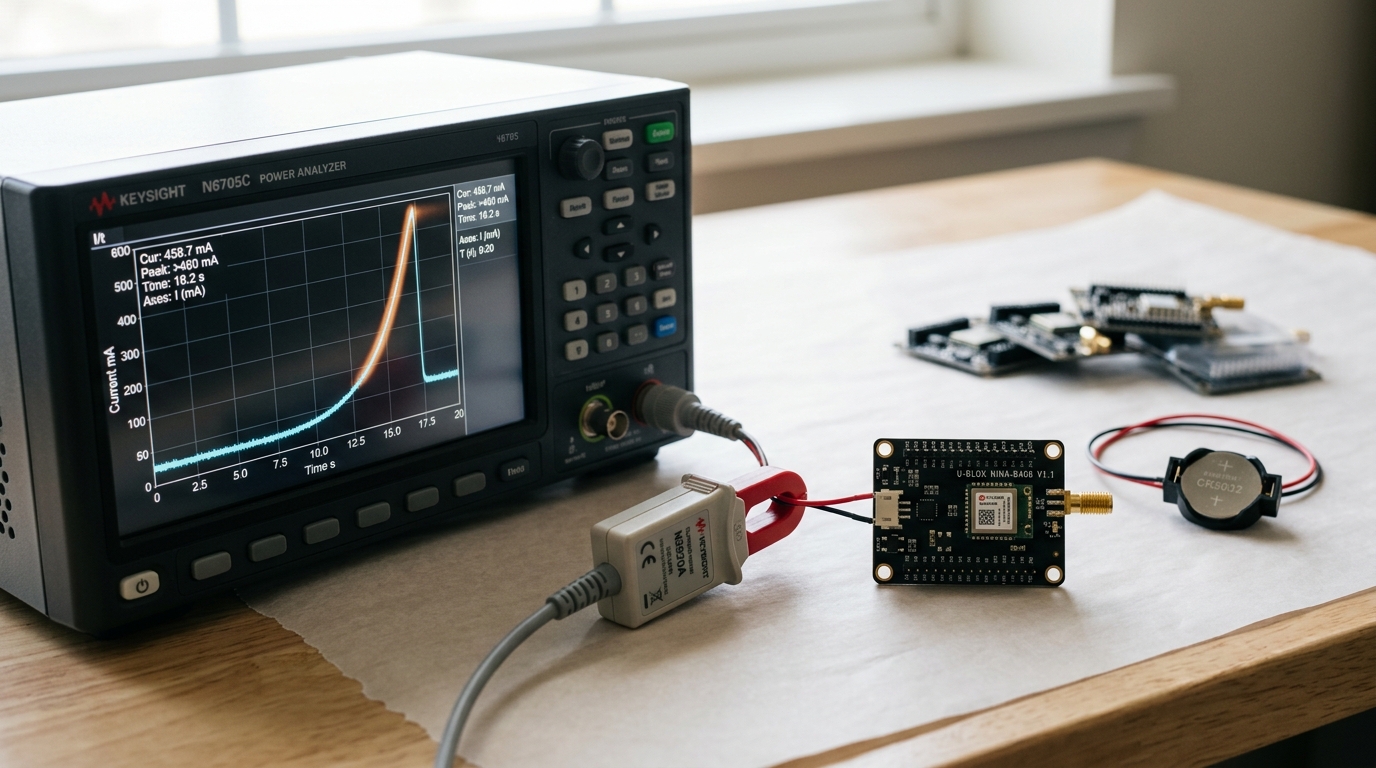
Figure 4. A power analyzer's current trace caught mid-transition, rising from the microcontroller's sleep floor toward an inference spike that has not yet peaked. — Image prompt and art direction by Brecht Corbeel; generation pending.
Privacy as a systems property, not a slogan
A frequent claim made about edge AI is that keeping inference local is inherently more privacy-preserving than sending raw sensor data to a server, because raw audio, imagery or biometric signals never leave the device. This is a real and mechanically grounded advantage — a system that classifies a wake word or a fall event on-device and transmits only the classification result has a measurably smaller data-exfiltration surface than one that streams raw audio continuously — but it is worth stating as a conditional property rather than an absolute one. A review of federated learning on edge sensing devices notes that privacy benefits in this class of system depend on the specifics of the deployment: what is actually transmitted off-device (a classification label versus a model gradient versus a compressed embedding), whether that transmission can itself leak information about the input through model-inversion-style attacks, and whether the on-device model or its updates are themselves ever centralized in a way that re-aggregates information the local-only design was meant to keep distributed [8]. The honest summary is that on-device inference removes one specific privacy risk (bulk transmission of raw sensor data) while leaving others (what a transmitted result reveals, how a shared model is trained or updated) as design choices that still have to be made deliberately rather than inherited automatically from “the AI runs on the device.”
Field reliability: what a bench-validated system still has to survive
A sensor system that meets its noise floor and power budget on a lab bench still has to survive conditions a bench does not reproduce. Three failure classes recur across fielded edge-AI hardware and are worth naming because none of them show up in a datasheet’s typical-conditions table. First, thermal drift: an analog front end’s offset and gain, and an ADC’s reference voltage, both shift with temperature, and a system calibrated once at room temperature will read differently at a temperature extreme unless it either recalibrates in the field or is characterized across its full operating range up front — this is precisely why data sheets like the AD7124-8’s specify performance across a temperature range (−40°C to 125°C) rather than at a single point [3]. Second, mechanical and connector fatigue: cable glands, board-to-board connectors and gasket seals degrade under repeated thermal cycling and vibration in ways a single bench test cannot reveal, which is why the lead-off detection circuitry documented in the ADS1298 exists at all — a system that can only assume its sensor connection stays good has no way to notice a slowly degrading contact until the data has already gone bad [5]. Third, event-rate and duty-cycle assumptions breaking under real conditions: a wake-on-motion or wake-on-event system tuned against a representative bench data set can still be surprised by an environment with more ambient triggering activity than the tuning set contained — vibration near a highway, insects near an outdoor camera, electrical noise near machinery — driving the system’s actual duty cycle, and therefore its actual average power draw, well above the number a lab characterization produced.
None of these are exotic failure modes; they are the ordinary cost of any physical system operating unattended for years rather than for the duration of a demo. The right response is not a single fix but a design discipline: instrument the connection itself (as lead-off detection does), specify and test across the real operating temperature range rather than trusting a single calibration point, and treat a duty-cycle assumption as a hypothesis to monitor in deployment rather than a fact established once on a bench.
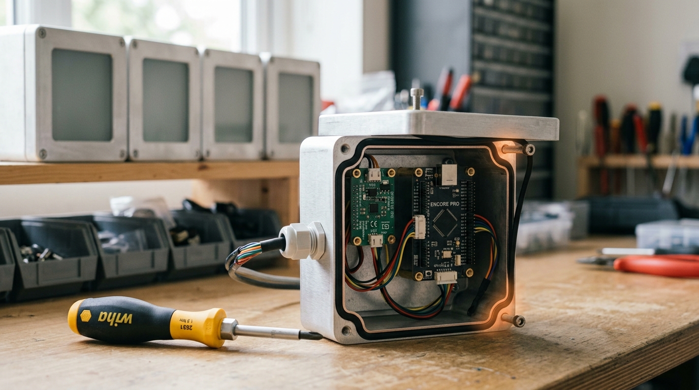
Figure 5. A field enclosure at the point of final assembly, one gasket edge still lifted a moment before the last screw seats it against weather and vibration. — Image prompt and art direction by Brecht Corbeel; generation pending.
A scenario, stated as a scenario
Consider a hypothetical outdoor wildlife-monitoring node built around an event camera and an IMU, powered by a small solar-charged battery, intended to run unattended for a full year between service visits. On the bench, its keyword-analogous “motion event” detector is tuned against a data set of recorded animal crossings and meets its target false-positive rate at a duty cycle low enough to project a comfortable multi-year battery life. In the field, ambient wind moving foliage generates a steady background of qualifying brightness-change events that the bench data set, recorded on a calm day, never contained — pushing the realized duty cycle several times higher than projected and the battery life down to a few months. This is a scenario, not a documented case, constructed to make concrete a failure mode this article has already described in the abstract (an event-rate assumption breaking under real conditions); it is offered as an illustration of the mechanism, not as a reported field result.
A dated prediction and its disconfirmation condition
Given the direction of the sensor and accelerator data sheets discussed here — event-rate controllers built directly into the sensor, motion-gated interrupt logic built directly into the IMU, and microNPUs sized in tenths of a square millimeter — a reasonable prediction, with a horizon of roughly three years from today (2026), is that mainstream always-on edge-AI product categories will increasingly push the “does anything need reporting” decision into sensor-adjacent mixed-signal circuitry rather than into software running on the main processor, extending the pattern the BMI270 and IMX636 already demonstrate to a wider range of sensor types. The assumption behind this prediction is that the dominant cost in always-on systems remains keeping a general-purpose processor awake rather than the cost of any individual inference. An observable indicator would be new microcontroller-class sensor data sheets increasingly advertising on-chip event or anomaly gating as a headline feature rather than an auxiliary one. The prediction would be disconfirmed if, instead, falling accelerator energy-per-inference numbers (of the kind MLPerf Tiny is built to measure independently) make always-running lightweight inference cheaper than dedicated wake circuitry, removing the incentive to push the gating decision into analog hardware at all.
Conclusion
An edge-AI sensor system is legible mechanism by mechanism, not as a single black box with a neural network inside it. An analog front end decides, before any digitization happens, what noise floor a signal can actually be resolved at. An event camera’s per-pixel asynchronous comparator circuit is a genuinely different device from a frame sensor’s clocked full-array readout, not just a different compression scheme applied to the same hardware. An always-on system’s power budget is an allocation across sensing, wake logic and inference, and the biggest lever available for meeting it is usually the wake logic, not the model. And a system validated on a bench still has to survive thermal drift, connector fatigue and duty-cycle assumptions that only a real deployment ever tests. None of this replaces model-level work — it is the physical layer that model-level work sits on top of, and it fails in its own ways, on its own schedule, regardless of how good the model is.
Sources
- Guillermo Gallego, Tobi Delbruck, Garrick Orchard, Chiara Bartolozzi, Brian Taba, Andrea Censi, Stefan Leutenegger, Andrew J. Davison, Jörg Conradt, Kostas Daniilidis, Davide Scaramuzza. Event-Based Vision: A Survey. IEEE Transactions on Pattern Analysis and Machine Intelligence (2022). DOI: 10.1109/TPAMI.2020.3008413.
- Thomas Finateu, Atsumi Niwa, Daniel Matolin, Koya Tsuchimoto, Andrea Mascheroni, Etienne Reynaud, Pooria Mostafalu, Frederick Brady, Ludovic Chotard, Florian LeGoff, Hirotsugu Takahashi, Hayato Wakabayashi, Yusuke Oike, Christoph Posch. A 1280x720 Back-Illuminated Stacked Temporal Contrast Event-Based Vision Sensor with 4.86um Pixels, 1.066GEPS Readout, Programmable Event-Rate Controller and Compressive Data-Formatting Pipeline. IEEE International Solid-State Circuits Conference (ISSCC) (2020). DOI: 10.1109/ISSCC19947.2020.9063149.
- Analog Devices Inc.. AD7124-8: 8-Channel, Low Noise, Low Power, 24-Bit, Sigma-Delta ADC. Analog Devices (2023).
- Bosch Sensortec GmbH. BMI270: Ultra-Low Power IMU. Bosch Sensortec (2021).
- Texas Instruments Inc.. ADS1298: Low-Power, 8-Channel, 24-Bit Analog Front-End for Biopotential Measurements. Texas Instruments (2017).
- Colby Banbury, Vijay Janapa Reddi, Peter Torelli, Jeremy Holleman, Nat Jeffries, Csaba Kiraly, Pietro Montino, David Kanter, et al.. MLPerf Tiny Benchmark. arXiv / Machine Learning and Systems (MLSys) proceedings (2021).
- Arm Limited. Arm Ethos-U55 NPU Technical Reference Manual. Arm (2023).
- Berrenur Saylam, Özlem Durmaz İncel. Federated Learning on Edge Sensing Devices: A Review. arXiv (2023).
Originally published at https://absolutedigitalpublishers.com/articles/how-edge-ai-electronics-and-sensor-systems-actually-works.