How Chiplets and Advanced Packaging Actually Work
A "chip" that ships today is often several dies stitched together after the fact. Here is how that stitching actually works — the interposers, the bonds, the standard that lets the dies talk, the stress that decides survival.
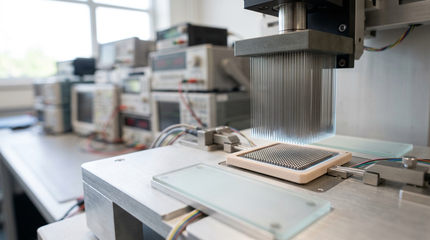
Before a package ships, it is proven on a bench like this one — testing whether the mechanics under its lid actually hold. — Image prompt and art direction by Brecht Corbeel; generation pending.
Abstract
This article is a mechanics walkthrough of advanced packaging: how a 2.5D silicon interposer routes signals between chiplets sitting side by side, how 3D hybrid bonding stacks dies with a direct copper-to-copper joint instead of solder, what the UCIe standard actually specifies for the electrical and protocol layers that let chiplets from different designs interoperate, and where coefficient-of-thermal-expansion mismatch, warpage, and known-good-die yield economics set the practical limits on how far this integration can be pushed. Every claim is tied to a named specification, conference paper, or vendor technical disclosure, with vendor performance claims marked as such and separated from measured, third-party-verifiable figures.
A modern high-end processor package is frequently not one chip. It is several — a compute die, one or more memory stacks, sometimes an I/O die, sometimes a piece of analog or radio-frequency silicon fabricated on a completely different process node — physically joined after each piece has already been made and tested. The reasons this happened are economic and are covered elsewhere in this pillar [6]. This piece is about the part that comes after the decision to disaggregate has been made: the actual mechanics of how those separate dies get put back together into something that behaves, electrically and thermally, like one part.
Three questions do almost all of the work. First, how do signals get from one die to the next — side by side on a shared carrier (2.5D), or stacked directly on top of one another (3D)? Second, if dies from different design teams or even different companies are going to sit on the same package, what standard governs the electrical and protocol handshake between them, so a compute tile and a memory tile that were never designed together can still be plugged in like matching parts? Third, once the mechanical and electrical connections exist, what physically limits how tightly this can be packed — and the answer to that third question turns out to be less about transistors and mostly about heat, expansion, and the economics of a bad bond.
2.5D: an interposer is a wiring layer, not a chip
The simplest form of advanced packaging places multiple chiplets side by side on a shared substrate called an interposer, rather than fusing them into one monolithic die. TSMC’s CoWoS (chip-on-wafer-on-substrate) family is the most widely deployed commercial example and is a useful concrete case because its structure is publicly documented. Individual dies are bonded through fine-pitch microbumps onto a silicon interposer; the assembly is then thinned to expose through-silicon vias (TSVs) running vertically through the interposer, C4 bumps are formed on the back side, and the whole assembly is bonded to a conventional package substrate [6].
The interposer itself carries no active logic. Its job is purely to be a very fine wiring layer sitting between the coarse-pitch package substrate below and the fine-pitch dies above. Two routing mechanisms do the work, and it is worth being precise about which one does which job: a redistribution layer (RDL) fans signals out laterally across the interposer’s surface, connecting a chiplet’s fine-pitch bumps to a neighboring chiplet sitting a few millimetres away on the same plane; TSVs then carry that same signal vertically down through the body of the interposer to the coarser bumps that meet the package substrate below. A chiplet only ever needs bumps at one pitch — its own, fine, native pitch — because the interposer’s TSVs and RDL together absorb the transition to the coarser pitch elsewhere [6].
This distinction matters for a practical reason: interposer size is reticle-limited. A silicon interposer is itself patterned like a chip, and a single lithographic exposure field (a reticle) caps how large a monolithic interposer can be — TSMC’s CoWoS-S variant is documented as accommodating interposers up to roughly 3.3 times a single reticle field, on the order of 2,700 mm² [6]. Packages that need to host more chiplets and more HBM memory stacks than that area allows move to CoWoS-L, which stitches several smaller reticle fields together using local silicon bridges embedded in a larger RDL interposer rather than paying for one continuous silicon interposer at full size [6]. That is a real engineering tradeoff, not a marketing distinction: a stitched interposer is cheaper per unit area and scales past the reticle limit, at the cost of a seam that has to be routed around and that introduces its own local mechanical discontinuity.
Vendor packaging brand names like CoWoS, and the specific reticle multiples and area figures associated with them, are vendor technical disclosures rather than independently audited specifications — they describe what TSMC states its process does, not a third-party measurement of it. The mechanism they describe (TSV-plus-RDL interposer routing) is the general 2.5D approach used, with variations, by essentially every major packaging house; the specific area limits and brand-name variants are TSMC’s own.
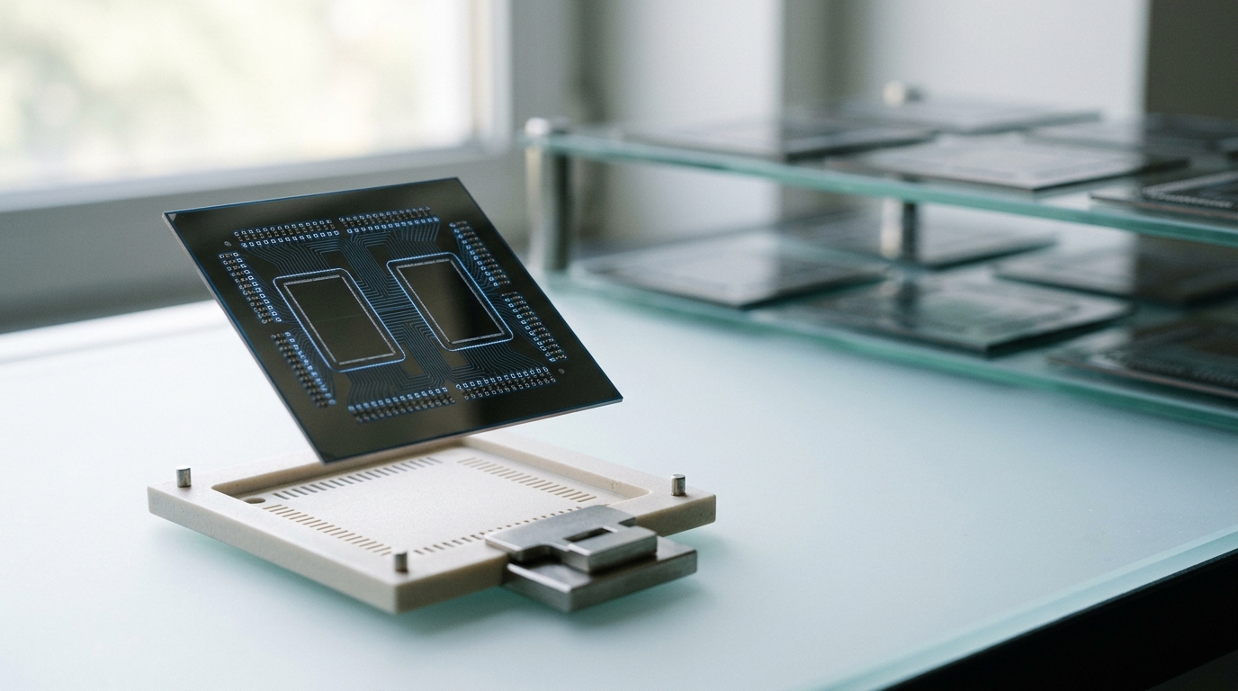
Figure 1. The interposer is a wiring layer with no logic of its own — through-silicon vias down, redistribution routing across. — Image prompt and art direction by Brecht Corbeel; generation pending.
3D: hybrid bonding replaces solder with a direct copper joint
2.5D integration keeps every die in the same plane. 3D integration stacks dies directly on top of one another, and the technology that has displaced solder microbumps for the tightest of these stacks is hybrid bonding: a direct, bump-less copper-to-copper connection formed without any intervening solder alloy.
The process, as described in industry technical accounts, happens in two distinct steps rather than one. First, the two die or wafer surfaces — each carrying a flat dielectric field with copper pads set slightly recessed into it — are brought together and bond at room temperature through a dielectric-to-dielectric (oxide-to-oxide, or in more recent flows, SiCN-to-SiCN) surface bond [7]. Second, the assembly is annealed. Under heat, the copper pads expand faster than the surrounding dielectric and press into direct contact, forming a true copper-to-copper metallic bond through solid-state diffusion [7]. No solder alloy is involved at any point, and consequently there is no reflow step, no underfill requirement, and — because there is no lower-conductivity solder joint sitting in the thermal path — a more direct thermal connection between the two stacked dies than a microbump joint provides.
The practical payoff of eliminating solder is pitch. Solder-based die-to-die bonding is reported to plateau in the 5–10 micron range; hybrid bonding is not similarly bounded by a solder alloy’s minimum reliable volume, which is why every actor in this space is pushing pitch down aggressively. AMD’s 3D V-Cache stacking uses a documented 9 micron hybrid-bond pitch, against a 130 micron pitch for conventional C4 bump packaging and roughly 50 microns for earlier microbump 3D approaches [9]. Intel’s Foveros Direct hybrid-bonding process is reported at sub-10 micron pitch in its early form, with a roadmap explicitly targeting below 5 microns to compete with 3D approaches at similarly aggressive pitches [8]. Research groups are well ahead of what has shipped in volume: imec has demonstrated die-to-wafer hybrid bonding at a 2 micron copper pad pitch with better than 350 nanometre overlay accuracy [2], and IBM Research has published microstructural work on copper bonding contacts scaled down to 0.8–4 micron diameters at 2–10 micron pitch spacings, studying how the copper itself deforms and diffuses at that scale [5].
Imec’s own framing of that result is worth quoting directly, because it states the tradeoff between die-to-wafer and wafer-to-wafer approaches precisely: die-to-wafer hybrid bonding “can now bridge the gap between solder-based die-to-die bonding (which is likely to stagnate at 10 to 5µm bump pitch) and wafer-to-wafer hybrid bonding,” according to imec R&D vice president Eric Beyne [2]. That framing also identifies why die-to-wafer bonding is preferred over wafer-to-wafer bonding for heterogeneous stacks specifically: it allows known-good dies of unequal sizes to be stacked with a higher compound yield, whereas wafer-to-wafer bonding commits every die position on a wafer to the pairing at once [2]. That known-good-die argument reappears below, because it is also the central economic argument for disaggregation in general.
One further physical detail is easy to miss and worth stating plainly: the “3D” stack is not always logic on top of logic. AMD places dedicated structural silicon — silicon with no active circuitry — over its stacked cache dies using the same hybrid-bonding process, specifically to create a uniform stack height for downstream lidding and to provide a continuous thermally conductive path from the high-power compute die below up to the heatsink, since silicon conducts heat far better than the mold compound or air gap it replaces [9]. Hybrid bonding is being used here as much for mechanical and thermal engineering as for signal routing.

Figure 2. Hybrid bonding skips solder entirely — the two surfaces meet dielectric-to-dielectric first, copper to copper only after. — Image prompt and art direction by Brecht Corbeel; generation pending.
UCIe: what the standard actually specifies
Interposers and hybrid bonding solve the physical connection problem. They say nothing about whether a compute chiplet from one design team and a memory or I/O chiplet from another can actually exchange data correctly once physically connected — that is a protocol and electrical compatibility problem, and it is what the Universal Chiplet Interconnect Express (UCIe) specification exists to solve.
UCIe 1.0, the foundational release, specifies “the complete standardized die-to-die interconnect with physical layer, protocol stack, [and] software model,” explicitly built to reuse established PCIe and CXL protocol layers above the new physical layer rather than inventing a new protocol stack from nothing [1]. That layering choice is significant: it means a UCIe link can carry ordinary PCIe or CXL traffic across a package-internal die-to-die connection using largely the same protocol-layer software and IP that already exists for board-level PCIe, with only the physical layer — the actual electrical signaling across the package substrate or interposer — being new.
The specification defines two distinct physical-layer targets tied to two different packaging tiers, and the numbers are precise enough to be worth stating exactly: UCIe-Standard Package (UCIe-S) targets a 110 micron bump pitch for conventional organic-substrate packaging, while UCIe-Advanced Package (UCIe-A) targets a much finer 45 micron bump pitch for 2.5D interposer or bridge-based packaging [1]. Bandwidth density scales directly with that pitch reduction — going from 110 to 45 microns substantially increases both raw die-edge bandwidth and bandwidth per unit silicon area, because more electrical lanes fit across the same edge length [1]. Later revisions extend the standard beyond 2.5D: UCIe 2.0 adds explicit 3D packaging support, describing bump pitches “as big as 10–25 microns to as small as 1 micron or less” for hybrid-bonding-based 3D stacks, and states that 3D packaging in general offers higher bandwidth density and power efficiency than 2D or 2.5D architectures at the same protocol layer [1]. UCIe 3.0 raises the per-lane data rate further, to 48 and 64 gigatransfers per second, doubling UCIe 2.0’s 32 GT/s [1]. UCIe 1.1 is described as an incremental reliability improvement over 1.0 rather than a new electrical tier [1].
It is worth being explicit about what this standard does and does not guarantee. UCIe compliance means two chiplets can establish a working electrical link and exchange PCIe- or CXL-framed traffic across it — it is an interoperability floor, not a performance ceiling, and not a guarantee that any two arbitrary UCIe-compliant chiplets will perform well together. A retimer mechanism exists in the specification specifically to extend UCIe connectivity beyond a single package using off-package electrical or optical links, with each retimer implementing a full UCIe interface on its own local side and independently negotiated buffer credits — a detail that matters because it signals the standard’s authors anticipated multi-package, not just single-package, chiplet topologies [1]. Whether that extended, off-package use case sees real deployment volume is a separate, open question this standard’s existence does not settle.
\text{link bandwidth} \approx N_{\text{lanes}} \times \text{data rate per lane} \times \frac{\text{module width}}{\text{bump pitch}}
This relation is not a UCIe-published formula; it is included here only to make explicit why bump pitch appears so often in vendor and standards disclosures as the headline number. For a fixed die edge length available to a module, halving the bump pitch roughly doubles the number of lanes that fit across that edge, and bandwidth scales accordingly — which is exactly why the standard defines separate pitch tiers for standard versus advanced packaging rather than one pitch for both.
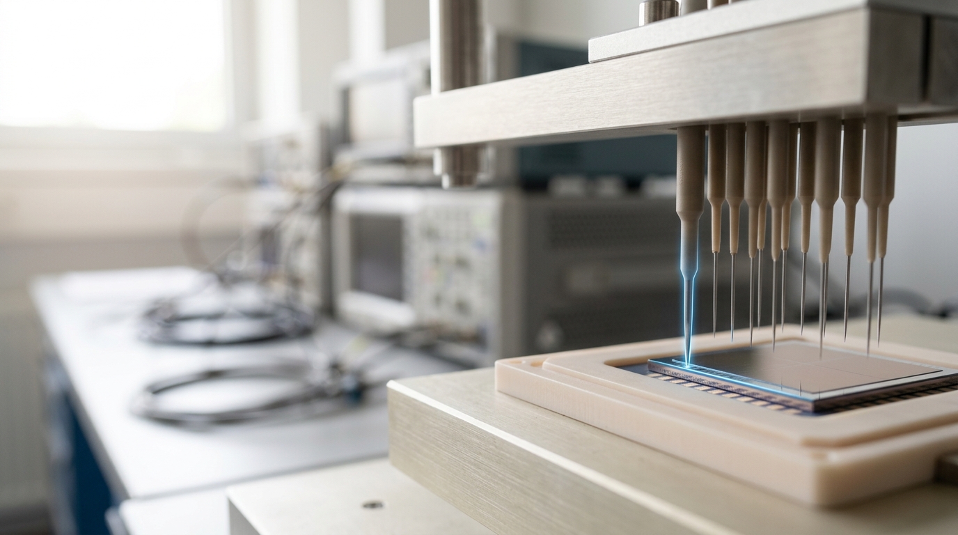
Figure 3. UCIe standardises what happens at this edge — the physical layer, the link training, the protocol stack above it — so dies from different vendors can still talk. — Image prompt and art direction by Brecht Corbeel; generation pending.
The thermomechanical limit: why this cannot simply keep shrinking
Interposer routing and hybrid bonding both trend toward finer pitch and tighter integration. The limit on how far that trend can go is set less by lithography than by the mechanics of putting several different materials — silicon, copper, mold compound, ceramic or organic substrate, underfill — into intimate, permanent contact and then cycling that assembly through large temperature swings for years.
The proximate cause is coefficient-of-thermal-expansion (CTE) mismatch. A 2024 review in Frontiers in Electronics identifies CTE mismatch within the die–mold–carrier stack as the dominant driver of warpage, particularly acute after post-mold curing, and notes that mold compound itself behaves viscoelastically — its internal stress does not resolve instantly but relaxes gradually over time and temperature, so warpage measured immediately after a process step is not necessarily the warpage the package will show later [3]. The review also identifies specific process moments where this bites hardest: wafer debonding, where stress accumulated through prior processing is suddenly released and redistributes across the thinned wafer, and backgrinding and RDL fabrication, which both add their own incremental stress [3]. Mitigation, per that review, runs through three levers: matching CTEs more closely across the material stack, using higher-glass-transition-temperature mold compound (since a compound’s effective CTE falls as its glass transition temperature rises), and using carrier wafers with higher CTE and stiffness for better dimensional stability during processing [3].
Why warpage matters is not cosmetic. The review states plainly that warpage “plays a critical role in determining whether an advanced package can be assembled successfully and meet long-term reliability targets,” and that warpage-induced package stress can alter electrical timing and voltage margins even in an assembly that passed initial test [3]. A package can be electrically functional at final test and still be carrying enough residual stress to fail a reliability qualification months later.
Placement — which chiplet sits where on the interposer — is not just an electrical routing decision either; it is a thermal and mechanical one simultaneously, and the two pull in different directions. Recent modeling work (STAMP-2.5D) makes a specific, testable claim about the coupling: that temperature gradients across an interposer, not absolute temperature levels, are the primary driver of the mechanical stress that heterogeneous chiplet assemblies experience, because gradients translate directly into differential CTE-driven expansion between adjacent regions [4]. Under that framing, a naive placement that simply packs the hottest chiplets as tightly as possible to minimize wire length can produce sharp local temperature gradients and correspondingly concentrated stress, even if the average package temperature looks acceptable. The same modeling work reports that placement optimized jointly for thermal and structural objectives reduced stress by close to 20 percent in one benchmark configuration relative to a thermal-only-optimized placement, while keeping temperatures within an acceptable range [4]. That specific percentage is a simulation result from one benchmark set, not a general physical constant, and should be read as illustrative of the coupling rather than as a number that transfers to any other package.
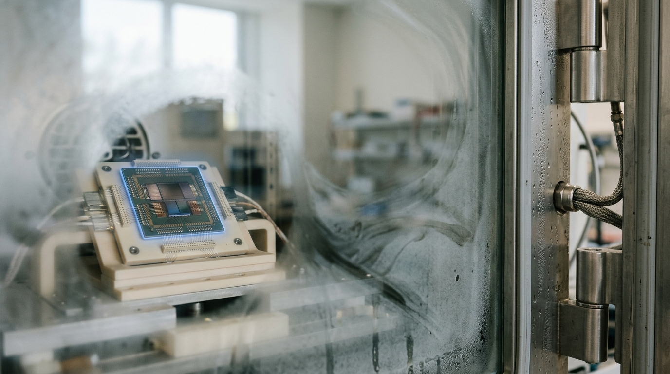
Figure 4. The package survives assembly; whether it survives years of thermal cycling between idle and full load is a separate, slower test. — Image prompt and art direction by Brecht Corbeel; generation pending.
Yield, known-good die, and why bad economics look like a mechanics problem
The last limit is economic, but it expresses itself as a packaging decision, which is why it belongs here rather than in a separate discussion. Every joining technology described above — microbump, hybrid bonding, interposer routing — creates a permanent, essentially unrepairable connection. A defect discovered after that connection is made does not cost one bad die; it can cost every die committed to that same assembly.
This is the direct rationale, stated by imec’s own R&D leadership, for preferring die-to-wafer hybrid bonding over wafer-to-wafer bonding for heterogeneous stacks: die-to-wafer bonding permits stacking known-good dies of unequal sizes, achieving a higher compound yield than committing an entire wafer’s worth of die positions to a single bonding pass [2]. The underlying arithmetic is straightforward and worth making explicit, because it is the actual reason “known-good die” testing exists as a discipline: if a stack of n dies each independently has yield y, and defects are uncorrelated across dies, the compound yield of the finished stack before any pre-screening is approximately y^n — falling multiplicatively with every additional die stacked. Testing and discarding bad dies before they are committed to an irreversible bond recovers the yield loss that would otherwise compound across the stack, at the cost of the test infrastructure itself: burn-in racks, edge probing at package-relevant pitch, and — increasingly, as hybrid-bonding pitch falls below what a needle probe can reliably contact — specialized fine-pitch test structures built into the die specifically to make pre-bond testing possible at all.
That testing cost is not free, and it does not fall to zero as pitch shrinks; if anything it rises, because a 2 micron hybrid-bond pad is a much harder electrical test target than a 45 micron UCIe advanced-package bump. This is a real, underappreciated tension in the roadmap toward finer pitch: the same scaling that increases bandwidth density and lowers per-bond thermal resistance also makes the pre-bond screening step that protects yield progressively harder to perform. None of the sources reviewed here quantify where that tradeoff crosses over into being uneconomical at current pitches; it is stated as a directional pressure by the packaging community, not as a solved problem, and readers should treat it as an open engineering question rather than a settled one.

Figure 5. When a bond fails, this is where the answer lives — a polished cross-section showing whether the copper actually joined or left a void. — Image prompt and art direction by Brecht Corbeel; generation pending.
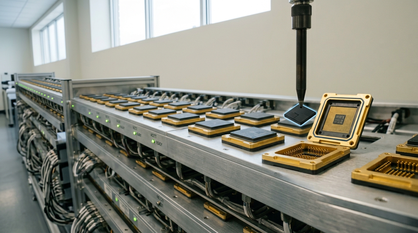
Figure 6. Yield economics push the hard sorting earlier — proving each die good before it is committed to a package it cannot be pulled out of again. — Image prompt and art direction by Brecht Corbeel; generation pending.
What this mechanics actually implies, and what would prove it wrong
Pulling the three threads together: 2.5D interposer routing and 3D hybrid bonding are both, at root, answers to the same underlying problem — get a signal from one piece of silicon to another without paying for a monolithic die that includes both — solved along different axes (lateral routing through an interposer versus vertical stacking through a direct bond). UCIe exists so that the dies on either side of that connection do not both have to come from the same design team to interoperate correctly. And the practical ceiling on all of it is not primarily an electrical engineering limit; it is a materials and economics limit, expressed as CTE-driven stress that degrades reliability, and as compounding yield loss that pre-bond testing exists specifically to contain.
A reasonable, falsifiable expectation follows from this: over roughly the next three to five years, expect hybrid-bonding pitch in shipping products to continue converging toward the low single-digit micron range that imec and IBM Research have already demonstrated in the lab, but expect the pace of that convergence in commercial products to lag the research demonstrations by several years, specifically because pre-bond known-good-die test infrastructure at those pitches has to mature in parallel — it is not a step that can be skipped. The observable indicator to watch is not a headline pitch number from a lab demonstration; it is whether packaging houses and OSATs begin publicly disclosing fine-pitch pre-bond test capability, since that is the gating step rather than the bond itself. If shipping products reach sub-2-micron hybrid-bond pitch in volume without any corresponding disclosure of new pre-bond test capability, that would be a signal this analysis is wrong about where the real bottleneck sits — for instance, because in-line inspection or built-in self-test structures on the die itself turned out to substitute for external probing more completely than assumed here.
Where the packaging and standards communities visibly disagree is less about whether hybrid bonding will keep scaling — most technical sources agree it will — and more about pacing and about whether 2.5D interposer approaches will be displaced by 3D stacking or will persist alongside it for different classes of chiplet. Nothing in the sources reviewed here settles that; it is characterised here as an open disagreement rather than resolved in either direction, because the evidence for a single winning topology is not there yet.
Sources
- UCIe Consortium. UCIe Specifications. UCIe Consortium (2025).
- Imec. Imec Demonstrates Die-to-Wafer Hybrid Bonding with 2µm Cu Interconnect Pad Pitch. Imec (2024).
- Frontiers in Electronics contributors. Warpage in wafer-level packaging: a review of causes, modelling, and mitigation strategies. Frontiers (2024).
- arXiv preprint authors. STAMP-2.5D: Structural and Thermal Aware Methodology for Placement in 2.5D Integration. arXiv (2025).
- IBM Research. A Microstructural Investigation of Sub-1 µm Copper Bonding Contact Structures in Die-to-Wafer Hybrid Bonding. IBM Research (ECTC 2024) (2024).
- WikiChip contributors. Chip-on-Wafer-on-Substrate (CoWoS). WikiChip (2025).
- SemiAnalysis. Hybrid Bonding Process Flow — Advanced Packaging Part 5. SemiAnalysis (2024).
- WCCFTech staff. Intel Foundry Reveals Plans for 'Process Leadership' at Direct Connect 2025. WCCFTech (2025).
- Tom's Hardware staff. AMD Unveils More Ryzen 3D Packaging and V-Cache Details at Hot Chips. Tom's Hardware (2022).
Originally published at https://absolutedigitalpublishers.com/articles/how-chiplets-and-advanced-packaging-actually-works.