Comparing the Main Approaches to Post-CMOS, Neuromorphic, Photonic, and Quantum AI Compute
Neuromorphic chips, photonic matrix multipliers, quantum machine learning, and memristor crossbars sit at different maturity levels and solve different problems. This piece compares them structurally instead of forcing a single winner.
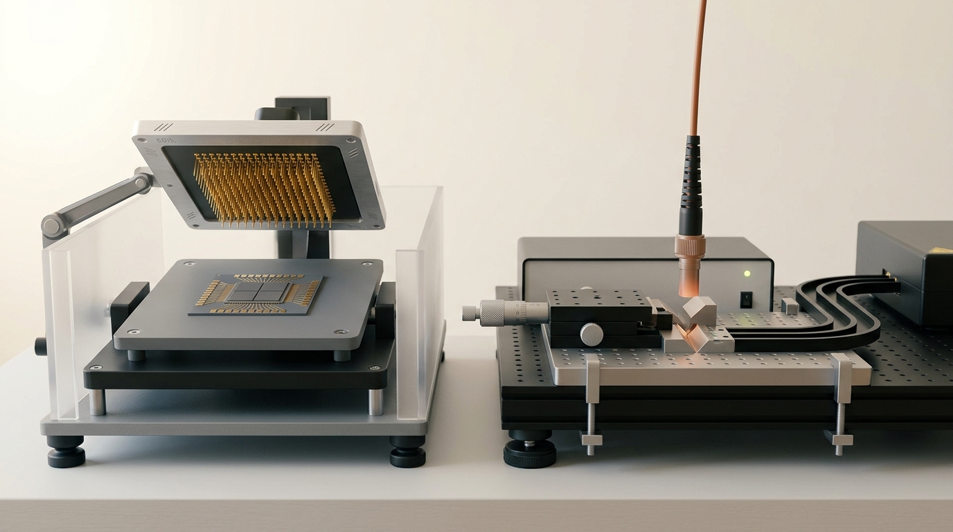
Two of the four approaches compared here, characterized on adjacent benches rather than reduced to one shared interface. — Image prompt and art direction by Brecht Corbeel; generation pending.
Abstract
This article compares the main non-incumbent bets for the future of AI compute — neuromorphic and spiking architectures, photonic matrix-multiply accelerators, quantum machine learning, and memristor-based analog in-memory compute — against each other and against the CMOS-scaling-plus-advanced-packaging baseline they are trying to unseat. Rather than ranking them on one scale, it classifies each by demonstrated maturity (research-stage, early-commercial, or largely aspirational relative to its own marketing), names the narrow workloads where each has shown a genuine, reproducible edge, and explains why several of the most-cited comparisons between them are not meaningful, because the approaches are being evaluated under incomparable conditions.
Five bets, one baseline, and a rule against forcing a winner
Every AI accelerator shipping into a datacenter or a phone today is, at the transistor level, the same kind of device: a CMOS chip, made faster not through a change in underlying physics but through denser transistors, chiplets glued onto an interposer, and dies stacked and bonded directly onto each other. That baseline — continued CMOS scaling delivered through advanced packaging rather than through the shrinking of a single monolithic die — is covered in depth elsewhere in this publication and is not re-derived here. It matters to this article only as the thing every alternative below is implicitly measured against, because it is the incumbent that has to become uneconomical, or run into a genuine physical wall, before any of the following four approaches gets adopted for anything beyond a defended niche.
This article compares four of the more serious non-incumbent bets: neuromorphic and spiking architectures, photonic matrix-multiply accelerators, quantum machine learning, and memristor-based analog in-memory compute. The instinct on encountering four alternatives to a dominant technology is to build a single table and pick a winner. That instinct is wrong here, and explaining why is most of the point of a comparison piece rather than a survey. A neuromorphic chip built to keep a hearing aid running for a week on a coin-cell battery is not competing with a quantum processor that requires a dilution refrigerator, a helium supply chain, and a team of cryogenic engineers to operate. Photonic accelerators are, so far, almost entirely about linear algebra — the one operation light is unusually good at — while memristor crossbars store a trained weight matrix physically as conductance and read it out through Ohm’s and Kirchhoff’s laws rather than through a stored program. Putting all four in one column of numbers implies they were measured under comparable conditions, and for most of the comparisons a reader is likely to encounter, they were not.
So this piece asks two questions separately for each approach, rather than one ranking once. First, the demonstrated maturity level: is there a peer-reviewed result on real hardware, a shipping commercial product, or mostly a roadmap and a press release? Second, is there a workload, however narrow, where the approach has shown a genuine, reproducible edge over the CMOS baseline, as opposed to an edge over a baseline the vendor chose to make itself look good? Only after answering both for all four does the piece turn to the comparisons that are not meaningful, and to what would actually have to change for that to stop being true.
The baseline these four are trying to unseat
Continued CMOS scaling has not stopped; it has changed shape. Rather than a single die shrinking uniformly at each process node, the industry has spent the last decade moving area, thermal budget, and yield risk around a package: splitting one large design into smaller chiplets, joining them through an interposer or direct wafer bonding, and stacking memory or logic vertically. The IEEE International Roadmap for Devices and Systems’ 2024 “More Moore” update describes the transistor side of this continuing along familiar lines — the industry-wide move from FinFET toward gate-all-around architectures, and power delivery migrating to the back side of the die to reclaim area without shrinking a critical dimension [1]. None of that requires new device physics. It is the same charge-based, digitally clocked transistor the industry has scaled for half a century, packaged more cleverly.
That is the correct baseline for everything below, for a specific reason: the CMOS-plus-packaging path has a known cost curve, a known software stack — every major machine learning framework already targets it — and a known manufacturing base spanning several foundries. Every approach below is, in effect, arguing that some part of that cost curve — energy per operation, cost per transistor, or memory bandwidth — is approaching a wall CMOS-plus-packaging cannot get past economically, at least for some workload. None of the four answers is “yes, unconditionally, starting now.”
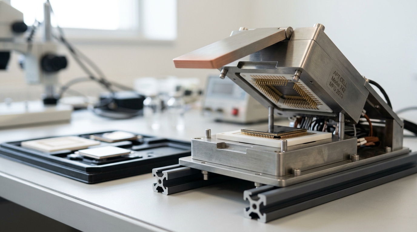
Figure 1. The baseline every alternative in this piece is measured against — CMOS scaling delivered through chiplets and packaging rather than a new device physics. — Image prompt and art direction by Brecht Corbeel; generation pending.
Neuromorphic and spiking architectures: mature enough to ship narrow, not mature enough to generalize
Neuromorphic hardware borrows two ideas from biological brains that conventional accelerators do not use: computation and memory that sit physically next to each other rather than being separated by a bus, and, in the strictest versions, communication through discrete, asynchronous spikes rather than a shared clock. The two ideas do not have to travel together, and the current generation of hardware splits cleanly along that line.
Intel’s Loihi 2, announced in September 2021 and fabricated on a pre-production version of Intel’s “Intel 4” process, is the clearer example of the second idea: up to 128 fully asynchronous neuro cores per chip supporting up to one million programmable spiking neurons, communicating over an on-chip and off-chip spike-event network rather than a global clock. Intel reports up to ten times faster processing and fifteen times greater resource density than the original Loihi, and, on a nine-layer inference workload, more than a sixtyfold reduction in operations per inference without a loss of accuracy [2]. Those are vendor-reported figures from Intel’s own announcement, not an independently audited benchmark, and should be read as a claim about Intel’s chip against Intel’s predecessor rather than about neuromorphic hardware against CMOS accelerators generally.
IBM’s NorthPole, described in a Science paper in October 2023 and at the 2024 International Solid-State Circuits Conference, is the clearer example of the first idea without the second. NorthPole descends architecturally from IBM’s earlier, genuinely spiking TrueNorth chip, but IBM’s own account is explicit that NorthPole itself moved to a synchronous, clocked digital architecture: 256 cores, each capable of 2,048 eight-bit operations per cycle, with memory distributed next to compute across the die rather than accessed over an external bus [3] [4]. IBM reports the chip as roughly 25 times more energy-efficient than 12-nanometer GPUs and 14-nanometer CPUs on ResNet-50 classification, and around 4,000 times faster than TrueNorth, with additional testing on YOLOv4, BERT, and DeepSpeech2 [4] — again IBM measuring IBM’s chip against chips and workloads IBM chose, a real peer-reviewed result about near-memory placement, not a neutral cross-vendor ranking.
SpiNNaker2, developed at TU Dresden and described in a 2024 paper, sits between the two: a digital chip built to support both genuinely event-based spiking workloads and conventional artificial neural networks on the same silicon, scaling into systems of many thousands of chips [5].
The workload fit actually demonstrated across all three designs is narrower than “AI compute” as a category: always-on, low-duty-cycle sensing, where most of the input is silence or a static scene, and the win comes from doing almost nothing, almost all of the time. Keyword spotting, gesture and event-camera vision, and other genuinely sparse, event-driven tasks are where spike-based computation’s actual advantage has a real workload to attach to. None of the three chips discussed here is available as a general-purpose commercial accelerator a customer can buy today for cloud-scale training or dense-batch inference; Loihi 2 and NorthPole are research chips distributed to partners rather than sold as products, and SpiNNaker2 is, on its own paper’s evidence, research-stage. Neuromorphic hardware in 2026 is research-stage with a narrow, real, already-demonstrated edge in sparse, always-on sensing, and no demonstrated edge yet in the dense, high-throughput workloads that dominate current AI infrastructure spending.
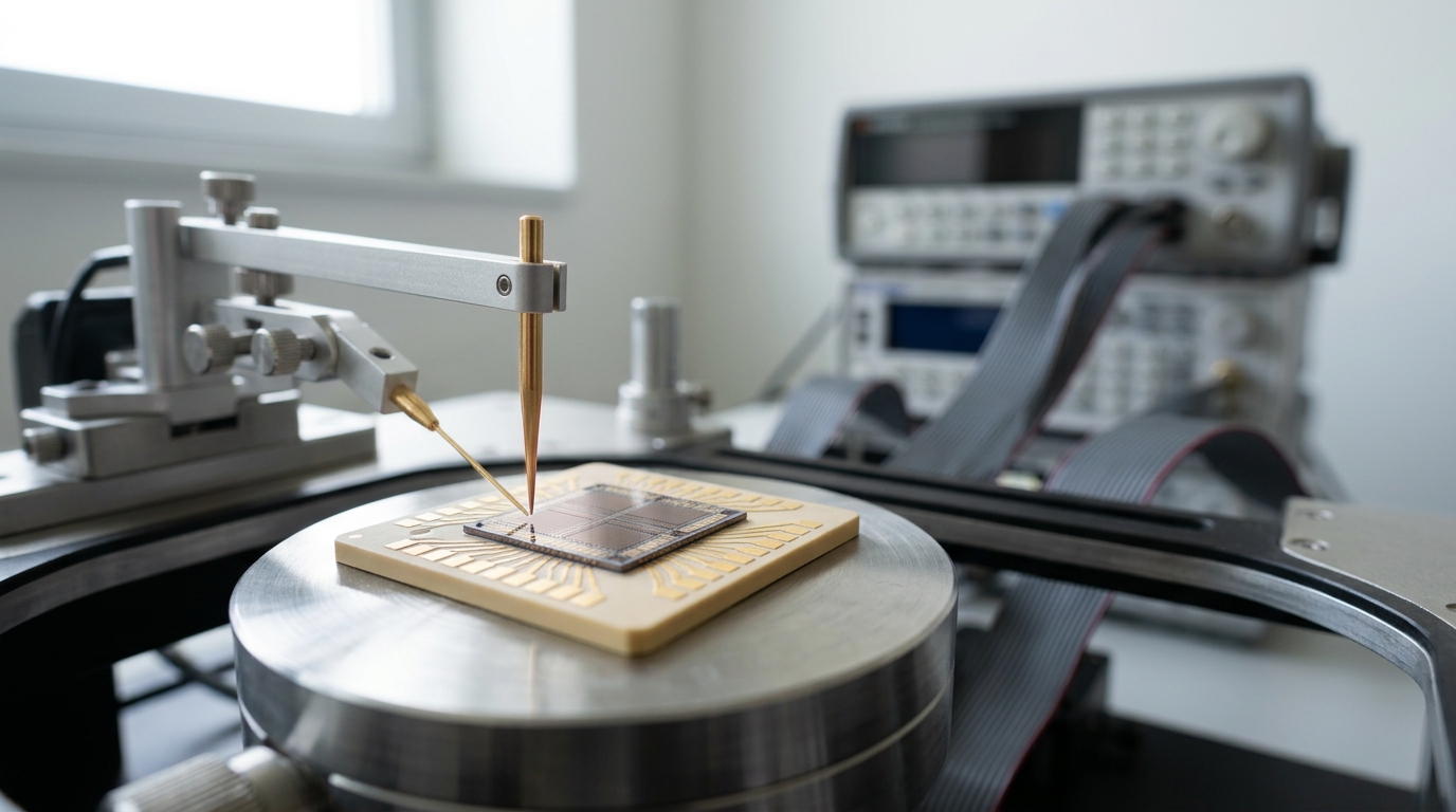
Figure 2. Loihi 2, NorthPole and SpiNNaker2 split the same brain-inspired idea two ways — near-memory placement and asynchronous spiking do not have to travel together. — Image prompt and art direction by Brecht Corbeel; generation pending.
Photonic matrix-multiply accelerators: fast at one operation, and only that operation
Photonic computing’s pitch is narrower than neuromorphic computing’s, and that narrowness is a genuine strength of the argument rather than a weakness. Light beams do not resist each other the way electrons in a wire do, and interference between beams passing through a mesh of tunable interferometers can implement a matrix-vector multiplication — the single most common operation in a neural network’s forward pass — as a physical, near-instantaneous process rather than a sequence of clocked arithmetic steps. The idea is not new: Shen and colleagues demonstrated a working optical neural network on a silicon photonic chip in 2017, using a cascaded mesh of 56 programmable Mach-Zehnder interferometers for vowel recognition, establishing the basic architecture most photonic accelerator designs since have elaborated on [6]. Feldmann and colleagues extended the idea in 2021 with a photonic tensor core combining phase-change-material memory with optical frequency combs, reporting operation above 14 gigahertz bandwidth and throughput in the trillions of multiply-accumulate operations per second on a convolutional processing demonstration [7].
Both results were academic demonstrations at small scale. The clearest evidence that photonic matrix multiplication has moved past proof-of-concept is a 2025 Nature paper describing a processor built by Lightmatter, with authors from both Lightmatter and OpenAI, reporting execution of ResNet, BERT, and an Atari deep-reinforcement-learning workload at near-electronic precision — a materially stronger claim than an internal vendor benchmark, because an outside AI lab ran recognizable workloads on the hardware rather than a hand-picked demonstration [8]. Lightmatter’s own account of its product line draws a maturity distinction worth taking at face value: the company describes its interconnect product, Passage, as approaching production deployment in 2026 with racks of hardware already shown publicly, while describing its compute accelerator, Envise, as “an essential step towards developing post-transistor computing technologies” rather than as a shipping product [9]. That is a vendor’s own characterization, but a candid one: photonic interconnect, which only has to move light-encoded data reliably between two points, is closer to commercial reality than photonic compute, which has to hold precision and thermal stability across a whole network’s forward pass.
The workload fit photonics has actually shown is specific: dense, regular, linear-algebra-dominated inference where a matrix stays fixed across many multiplications and precision requirements can tolerate optical noise and thermal drift. Photonic accelerators are not proposed as a replacement for a general-purpose processor; every design here is a co-processor inside a larger electronic system, because nonlinearities and control flow still have to happen in electronics. That makes photonic compute closer to an accelerator for one operation than a new kind of general AI chip, and its maturity sits at early-commercial for the interconnect variant, research-stage for the compute variant.
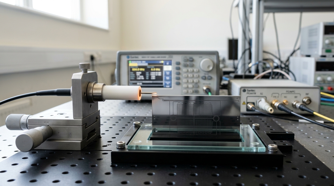
Figure 3. Photonic accelerators are fast at one operation, matrix multiplication by interference, and depend on conventional electronics for everything else a network needs. — Image prompt and art direction by Brecht Corbeel; generation pending.
Quantum machine learning: one genuine advantage, and it is not the one being sold
Quantum computing’s relationship to AI is the most frequently overstated of the four, and the overstatement has a specific, identifiable shape: a demonstrated exponential quantum advantage exists, but it is for learning about quantum systems from quantum data, not for accelerating the kind of machine learning done today on classical data such as text, images, or tabular records.
The advantage that has actually survived scrutiny comes from a 2022 Science paper by Huang, McClean, and colleagues at Google Quantum AI and collaborating institutions. Using up to 40 qubits on a superconducting processor, the experiment showed that a quantum learner able to store and jointly measure two copies of an unknown quantum state needed roughly ten thousand times fewer measurements than the best possible classical strategy to predict a property of that state to a given accuracy, an advantage the authors argue is information-theoretic and therefore robust even under today’s noise levels [11]. That is a real, peer-reviewed, and — within its stated scope — durable result. Its scope is the qualifier most popular coverage drops: the task is learning about a quantum system using quantum-generated data, a genuine niche in quantum chemistry, materials science, and sensing, not a description of what happens when a language model or an image classifier is run.
For quantum algorithms proposed to accelerate machine learning on ordinary classical data — the sense in which “quantum AI” is usually marketed — the evidence points the other way on two grounds. The first is trainability: McClean and colleagues showed in 2018 that for a wide class of the parameterized quantum circuits used in most proposed quantum machine learning models, the probability that a gradient in any direction is non-negligible shrinks exponentially with qubit count — a “barren plateau” that makes gradient-based training intractable at exactly the scale where an advantage would need to appear [12]. The second is the comparison baseline itself. In 2018, Ewin Tang showed that a quantum algorithm for recommendation systems, held up as one of the strongest candidates for exponential quantum speedup, could be matched, up to polynomial factors, by a classical algorithm nobody had previously constructed:
T_{\text{classical}} = O\!\left(\mathrm{poly}(k)\log(mn)\right) \approx T_{\text{quantum}},
where the classical algorithm samples from an \ell^2-norm-weighted data structure rather than reading the whole m \times n matrix, closing a gap previously measured only against a classical algorithm that read every entry [13]. The general lesson, sometimes called dequantization, is that an apparent exponential quantum speedup often measures the gap between a quantum algorithm and an unnecessarily weak classical baseline, and the gap can close once someone finds a better classical algorithm.
Maturity compounds both problems. Every quantum processor operating today, including IBM’s fleet of more than ninety systems, is what John Preskill named in 2018 the “noisy intermediate-scale quantum,” or NISQ, regime: enough qubits to be interesting, not enough error correction to run a precise computation without the answer being swamped by noise [10]. IBM’s own roadmap expects a first instance of quantum advantage alongside high-performance classical computing in 2026, and targets 2029 for Quantum Starling, its first planned large-scale fault-tolerant machine, backed by a stated commitment of more than ten billion dollars [14]. Those are the vendor’s own targets, not independently verified outcomes. Taken together, the honest maturity assessment for quantum machine learning on classical AI workloads in 2026 is research-stage bordering on aspirational for the claim most often marketed, and a narrow, genuinely demonstrated research-stage advantage for the quantum-data learning tasks the Huang et al. result actually covers.
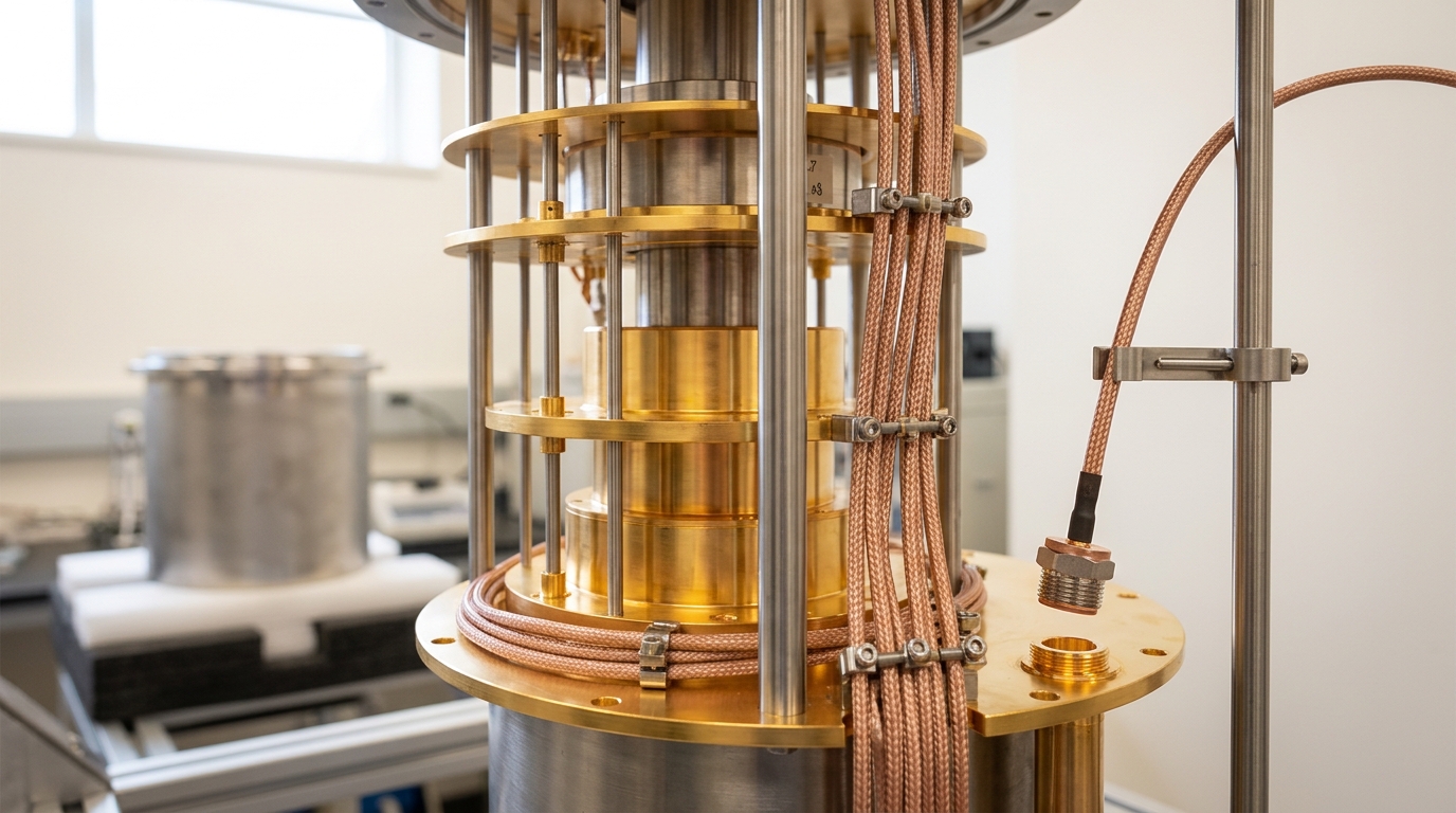
Figure 4. Every quantum processor operating today is a pre-fault-tolerant, noisy intermediate-scale machine — the maturity gap the marketing usually skips. — Image prompt and art direction by Brecht Corbeel; generation pending.
Memristor and analog in-memory compute: the closest thing to just replacing the multiply
Of the four approaches, memristor-based and other analog in-memory designs make the narrowest and most literal claim: store a trained weight as a physical conductance in a crossbar array, and perform the dominant operation in a neural network’s forward pass — multiply-and-accumulate — as a single physical step using Ohm’s law for the multiplication and Kirchhoff’s current law for the accumulation, rather than as a sequence of digital arithmetic operations that each have to move data between memory and a separate compute unit.
The device class was given a physical demonstration in 2008, when Strukov, Snider, Stewart, and Williams at HP Labs showed that a fourth fundamental circuit element predicted on symmetry grounds by Leon Chua decades earlier — a resistor whose resistance depends on the history of charge passed through it — arises naturally in nanoscale systems where electronic and ionic transport are coupled [15]. The more recent, directly AI-relevant demonstration uses a related but distinct mechanism: phase-change memory, storing a weight as the electrically read resistance of a material switched between crystalline and amorphous states rather than as an ionic memristor. IBM’s 2023 Nature paper describes a chip built from 35 million phase-change memory devices across 34 tiles, reporting up to 12.4 tera-operations per second per watt in chip-sustained performance, and, on a speech-transcription workload using a recurrent neural network transducer with 45 million weights spread across five chips, a fourteenfold improvement in energy efficiency over the best result submitted to MLPerf for that task, while keeping accuracy within an acceptable margin of a conventional digital implementation [16]. That fourteenfold figure is one of the more directly comparable numbers in this piece, precisely because it was measured against an external, standardized benchmark submission rather than a baseline the authors chose themselves — the same MLPerf suite used throughout this article as a reference point for what an audited, cross-vendor comparison looks like [18].
On the commercial side, Mythic is the clearest example of an analog compute-in-memory company selling into production rather than describing a research chip. Mythic’s own technology page describes an architecture combining compute-in-memory, a dataflow execution model, and analog computation in a tiled design aimed at edge inference in surveillance, drones, and robotics, with tooling for standard machine learning frameworks already available [17]. That is a vendor’s self-description rather than an audited shipping-volume figure, and is presented here as a claim, not a verified fact.
The physical limitation keeping analog in-memory compute confined to inference on weights that rarely change is the flip side of its core trick: a conductance that can be read out to represent a weight can also drift over time, and writing a new one wears the device in a way reading does not, so retraining costs more, in time and device lifetime, than in a design where weights sit in ordinary digital memory. A simple accounting for why raw operations-per-watt numbers are not directly comparable across any of the four approaches in this piece is worth writing out once:
E_{\text{op}} = E_{\text{core}} + E_{\text{periphery}} + E_{\text{I/O}},
where E_{\text{core}} is the energy of the operation itself — the multiply-accumulate, the interference pattern, the qubit gate — and E_{\text{periphery}} and E_{\text{I/O}} are the data-converter, laser-and-detector, cryogenic, or spike-routing overhead surrounding it. A headline figure reporting only E_{\text{core}}, which vendor materials frequently do, looks dramatically better than one reporting the whole sum, and each approach hides a different fraction of its true cost: analog crossbars in E_{\text{periphery}}'s data converters, photonics in E_{\text{I/O}}'s laser budget, quantum processors in E_{\text{periphery}}'s dilution-refrigerator overhead. A single tera-operations-per-watt figure without knowing which terms it includes is close to meaningless, and comparing two such figures from two vendors compounds the problem.
Taken as a whole, analog in-memory compute is early-commercial for narrow, static-weight edge inference, with the strongest externally referenced evidence in this piece — the MLPerf-referenced fourteenfold figure — and a well-understood physical reason, drift and write endurance, why it does not generalize to training or frequently updated models.
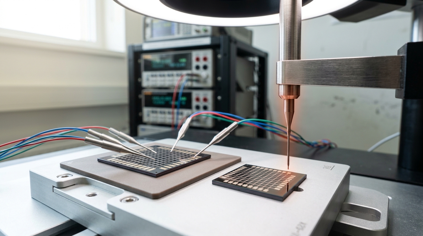
Figure 5. Analog in-memory compute stores a trained weight as a physical conductance and reads it out through Ohm's and Kirchhoff's laws rather than a stored program. — Image prompt and art direction by Brecht Corbeel; generation pending.
Why a single ranking is not available
Four maturity assessments and four workload-fit findings are the output of the sections above, not four points on one leaderboard, and the reasons are worth stating plainly rather than left implicit.
The four approaches are not being measured under comparable conditions in the sources available today, on three separate grounds. First, maturity itself varies too widely for a ranking to mean anything: Mythic ships a product; Loihi 2 and NorthPole are research chips distributed to partners; Lightmatter’s Envise has a peer-reviewed demonstration but its own maker declines to call it commercial; and every quantum processor in existence is, by its own vendors’ account, a pre-fault-tolerant machine not expected to reach even its maker’s own “genuine advantage” milestone before 2026, with fault tolerance itself not targeted before 2029 [14]. Ranking a shipping product against a 2029 roadmap target answers a different question than the one a reader asking “which is best” thinks they are asking.
Second, the workloads are not shared. Neuromorphic hardware’s demonstrated edge is sparse, event-driven, low-duty-cycle sensing. Photonic accelerators’ edge is dense, fixed-matrix linear algebra at inference time. Quantum’s one durable advantage is learning about quantum-generated data, a category that barely overlaps with commercial AI workloads. Memristor-based analog compute’s edge is static-weight edge inference where retraining is rare. A table listing all four against, say, “image classification throughput” is not comparing four solutions to one problem; for at least two of the four, it asks them to do something outside the workload where any evidence exists at all.
Third, and most concretely, none of the four alternative substrates discussed here currently submits results to MLPerf, the one standardized, audited, cross-vendor inference benchmark conventional CMOS accelerators compete on [18]. Every performance number available for neuromorphic, photonic, quantum, or memristor hardware in this piece comes from the vendor’s or research group’s own paper, under a baseline, workload, and set of reported metrics that group chose. This publication’s standing editorial rule against building a cross-vendor ranking out of numbers generated under different, self-selected conditions applies here without exception, and it is why this article does not produce a table ranking the four approaches against each other. Where a genuinely comparable number exists — IBM’s analog-AI chip measured against an external MLPerf submission is the clearest instance here — it is reported as such and flagged as unusually strong evidence precisely because it is the exception rather than the rule.
None of this means the approaches cannot be usefully described relative to a shared, informal notion of readiness. The three-level maturity classification used throughout this piece — research-stage, early-commercial, or largely aspirational relative to its own marketing — borrows loosely from the technology-readiness-level framework long used in aerospace and defense procurement to describe how far a technology has moved from a lab demonstration toward a fielded system, without claiming that framework’s formal, numbered precision. Used descriptively, it is enough to place Mythic’s shipping chips ahead of Loihi 2’s research samples, and those ahead of a NISQ-era processor’s roadmap slide, without pretending any of the three competes for the same design win.
Figure 6. Different maturity levels and different target workloads mean these approaches cannot be collapsed into one ranking — the comparison itself has to stay honest about that. — Image prompt and art direction by Brecht Corbeel; generation pending.
What would actually change this comparison
The four assessments above are current as of 2026, and each rests on assumptions that could change. Stated as falsifiable predictions rather than as forecasts dressed as certainty, with a shared horizon set to match IBM’s own fault-tolerance target:
One. Photonic interconnect will reach broader commercial deployment than photonic compute before the end of 2028, because Passage-class products only have to move already-digital signals reliably between two points using established foundry partnerships, while Envise-class products must hold calibration and precision across an entire network’s forward pass. Assumption: no photonic-compute vendor solves system-level calibration drift at scale in the interim. Indicator: named, priced photonic-compute SKUs available for general enterprise purchase, not research partnerships or pilots. Disconfirmed if a general-purpose photonic-compute product reaches commercial availability, with a published price and support contract, before an equivalent-maturity photonic-interconnect product does.
Two. No claimed quantum advantage on a classical-data machine learning task — as opposed to a quantum-data task in the mould of Huang and colleagues’ result — will survive a best-known-classical-algorithm comparison and independent replication before IBM’s own targeted fault-tolerant milestone around 2029. Assumption: NISQ-era gate error rates do not fall faster than current roadmaps project. Indicator: a peer-reviewed, independently replicated classical-data result that a subsequent dequantization attempt, in the tradition of Tang’s 2018 result, fails to match with a polynomial-time classical algorithm. Disconfirmed if such a result survives scrutiny before 2029, or if IBM’s fault-tolerant timeline slips by more than two years without one.
Three. A named analog in-memory or memristor-based inference chip will reach shipping volume in the hundreds of thousands of units before any spiking neuromorphic chip reaches an equivalent volume in a non-defense, non-research channel, because analog in-memory compute maps directly onto weight matrices networks are already trained to produce, while spiking hardware requires workloads re-expressed in an event-driven form most trained models do not natively have. Assumption: no toolchain emerges that converts trained networks into spiking form without an accuracy penalty large enough to block adoption. Indicator: an MLPerf-referenced or comparably audited efficiency figure for a shipping analog chip, matched against a disclosed shipping volume from a spiking-chip vendor. Disconfirmed if a spiking chip reaches comparable volume first, or if a peer-reviewed study documents drift or endurance failures severe enough to stall analog deployment first.
What to take away
Four alternatives to continued CMOS scaling are real, in the narrow sense that each has at least one peer-reviewed or externally referenced result behind it rather than only a roadmap slide. None is a general-purpose replacement for the CMOS-plus-packaging baseline it implicitly competes against, and none is best understood as competing directly with the other three. Neuromorphic hardware’s edge is sparse, always-on sensing, at a carefully chosen maturity point: ready for research partnerships, not yet for a general product line. Photonic compute’s edge is one operation, matrix multiplication, with its interconnect technology further along the path to market than the compute core itself. Quantum machine learning has exactly one durable, peer-reviewed advantage, for learning about quantum systems rather than the classical-data tasks the phrase usually implies in a pitch deck. Memristor-based analog compute has the single most externally referenced efficiency number in this piece, earned because it was measured against an audited outside benchmark rather than a self-chosen baseline, and a well-understood physical reason — drift, and the cost of rewriting a conductance — why that number does not generalize to training.
The honest version of “which of these wins” is not a ranking. It is a readiness map with four points on it, each answering to a different workload, moving at a different pace, and none of them yet answering to the same audited benchmark the CMOS baseline already competes on. Whether that changes is itself the thing worth watching, more than any individual number any one vendor publishes next year.
Sources
- IEEE International Roadmap for Devices and Systems. International Roadmap for Devices and Systems 2024 Update — More Moore. IEEE IRDS (2024).
- Intel Corporation. Intel Advances Neuromorphic with Loihi 2, New Lava Software Framework and New Partners. Intel Corporation (2021).
- Dharmendra S. Modha et al.. Neural inference at the frontier of energy, space, and time. Science (2023). DOI: 10.1126/science.adh1174.
- IBM Research. IBM Research's New NorthPole AI Chip. IBM Research (2023).
- Hector A. Gonzalez et al.. "SpiNNaker2: A Large-Scale Neuromorphic System for Event-Based and Asynchronous Machine Learning". arXiv (2024). DOI: 10.48550/arXiv.2401.04491.
- Yichen Shen et al.. Deep learning with coherent nanophotonic circuits. Nature Photonics (2017). DOI: 10.1038/nphoton.2017.93.
- J. Feldmann et al.. Parallel convolutional processing using an integrated photonic tensor core. Nature (2021). DOI: 10.1038/s41586-020-03070-1.
- S. R. Ahmed et al.. Universal photonic artificial intelligence acceleration. Nature (2025). DOI: 10.1038/s41586-025-08854-x.
- Lightmatter. Vision. Lightmatter (2026).
- John Preskill. Quantum Computing in the NISQ era and beyond. Quantum (2018). DOI: 10.22331/q-2018-08-06-79.
- Hsin-Yuan Huang et al.. Quantum advantage in learning from experiments. Science (2022). DOI: 10.1126/science.abn7293.
- Jarrod R. McClean et al.. Barren plateaus in quantum neural network training landscapes. Nature Communications (2018). DOI: 10.1038/s41467-018-07090-4.
- Ewin Tang. A quantum-inspired classical algorithm for recommendation systems. ACM Symposium on Theory of Computing (2019). DOI: 10.48550/arXiv.1807.04271.
- IBM. IBM Commits More Than $10 Billion to Quantum Computing, Funding Its Roadmap from Today's Leading Systems to the World's First Fault-Tolerant Quantum Computers. IBM Newsroom (2026).
- Dmitri B. Strukov, Gregory S. Snider, Duncan R. Stewart, and R. Stanley Williams. The missing memristor found. Nature (2008). DOI: 10.1038/nature06932.
- S. Ambrogio et al.. An analog-AI chip for energy-efficient speech recognition and transcription. Nature (2023). DOI: 10.1038/s41586-023-06337-5.
- Mythic, Inc.. Technology. Mythic, Inc. (2026).
- MLCommons. MLPerf Inference Datacenter Benchmark. MLCommons (2025).
Originally published at https://absolutedigitalpublishers.com/articles/comparing-the-main-approaches-to-post-cmos-neuromorphic-photonic-and-quantum-ai-compute.