Comparing the Main Approaches to Advanced Semiconductor Fabrication
EUV single exposure against DUV multi-patterning, FinFET against gate-all-around, and TSMC, Samsung and Intel's differing bets on sequencing both — set out as tradeoffs, not a ranking, with real disagreements left standing as disagreements.
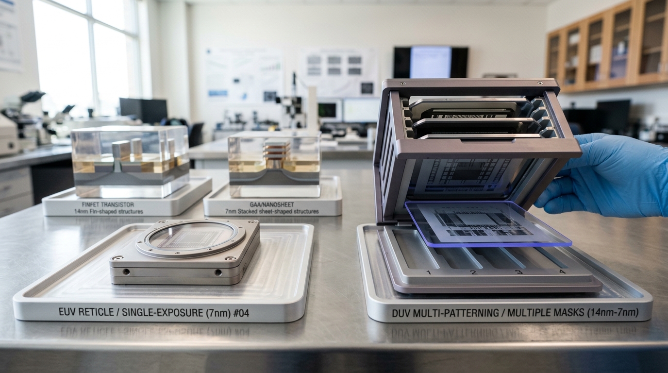
One exposure against several — the comparison this article draws is a controlled one, not a ranking, and it starts with what actually gets loaded onto the bench for each route. — Image prompt and art direction by Brecht Corbeel; generation pending.
Abstract
This article compares the main approaches to advanced semiconductor fabrication on three separate, only loosely coupled axes: how a critical layer's pattern gets printed (single-exposure EUV at high numerical aperture versus multi-pass DUV patterning), what shape the transistor takes (a vertical fin versus a horizontally stacked gate-all-around channel), and how TSMC, Samsung and Intel have each sequenced and combined those choices into a distinct process philosophy. It draws on IEDM and VLIS Symposium papers, imec and IRDS technical reports, manufacturer disclosures, and industry-analyst reporting, and it deliberately avoids building a cross-vendor ranking from incomparable yield rumors or vendor benchmarks — characterising instead the places, including a genuine peer-reviewed dissent on gate-all-around's advantages, where informed practitioners disagree about which approach wins and under what conditions.
Three separate bets, not one ranking
A node name like “3nm,” “2nm,” or “18A” bundles three genuinely separate engineering decisions into a single marketing label, and treating “TSMC versus Samsung versus Intel” as though it named one contest obscures more than it reveals. The first decision is how a critical layer’s pattern actually gets printed onto the wafer: with a single extreme-ultraviolet exposure at high numerical aperture, or by splitting the same pattern across several exposures at a lower, cheaper numerical aperture. The second is what shape the transistor’s channel takes: a vertical fin gated on three sides, or a stack of horizontal sheets gated on all four. The third is how a specific foundry sequences and combines the first two choices, and what else it bundles alongside them, into something that deserves to be called a process philosophy rather than a spec sheet.
These three axes are only loosely coupled, which is itself the first useful fact. A fab can print a gate-all-around transistor’s critical layers with either lithography strategy, and a fab can extend fin-shaped transistors well past the node where a competitor moved on. TSMC ran its N3 generation entirely on FinFETs after Samsung had already shipped gate-all-around devices at what both companies market as the same technology generation [11, 12]. None of the three axes has one winner across cost, yield risk, timeline, and performance at once, and where the published record shows genuine technical disagreement rather than merely competing marketing claims, this article says so rather than adjudicating it.
What a single exposure actually buys
The case for high numerical aperture extreme-ultraviolet lithography is, at bottom, a case about counting exposures. imec’s own comparison states it in mask counts: at the 0.33 numerical aperture used by today’s production EUV scanners, patterning critical metal layers with tight, sub-20-nanometre pitches at imec’s projected A14 and A10 logic nodes would require three to four separate masks, where a single exposure at 0.55 numerical aperture does the same layer in one pass; for the bitline-periphery and storage-node landing-pad layers of advanced DRAM, imec puts the current requirement at three masks against a single exposure at high numerical aperture [4]. Those are imec’s own projections for its own roadmap nodes, not measured production results, and they should be read as an institutional research lab’s assessment rather than a settled fact about any specific foundry’s flow.
What a mask count actually costs is not one extra exposure. It is an extra circuit through the entire patterning loop: another resist coat, another exposure, another develop, in most multi-patterning schemes another etch and clean, and another round of the metrology that has to confirm the result before the next layer can be trusted to sit on top of it. If a critical layer’s target pitch is split across N separately printable exposures — as litho-etch-litho-etch and self-aligned multiple patterning both do, in different ways — and each exposure contributes an independent, zero-mean placement error of standard deviation \sigma, the layer’s overlay-driven placement uncertainty combines in quadrature:
\sigma_N = \sigma\sqrt{N}.
Treat this as a simplified budgeting device rather than a physical law; real exposures on the same scanner and same reticle stage are not fully independent, and correlated error can be partly calibrated out. But the shape of the relation is the point. Going from one exposure to a four-way split does not merely quadruple the number of things that can go wrong in the abstract; under the idealised independence assumption it grows the placement-uncertainty budget by a factor of two, while genuinely multiplying the number of independent process passes — each with its own particle risk, its own drift, and its own measurement — through which the layer can fail. The International Roadmap for Devices and Systems’ 2023 lithography update draws the corresponding practical conclusion in its own language: “it has become clear that EUV will not replace multiple patterning. Both technologies will be used, and the choice of using multiple patterning or not will depend on level-specific details, yield, and cost” [3]. That is an institutional roadmap’s synthesis of the industry’s contributing members, not one vendor’s marketing position, and it is the closest thing to a consensus statement this comparison has.
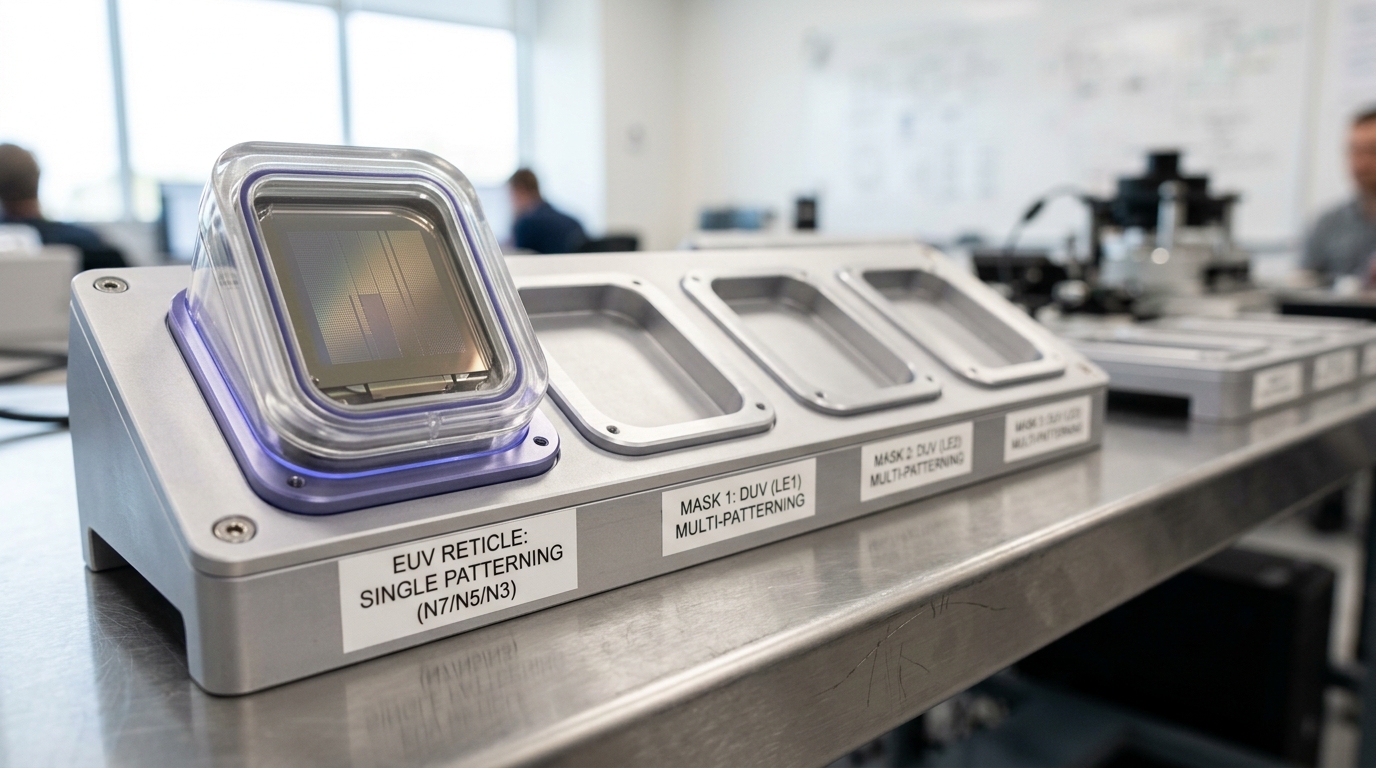
Figure 1. A single exposure replaces however many a critical layer would otherwise need — the comparison is visible in what is not on the tray, not only in what is. — Image prompt and art direction by Brecht Corbeel; generation pending.
ASML’s own specification for its first high-numerical-aperture scanner shows what a single exposure adds in the other direction. The TWINSCAN EXE:5000 raises numerical aperture from 0.33 to 0.55 and, ASML states, delivers 8-nanometre resolution — enough, the company claims, to print features 1.7 times smaller in a single pass and reach roughly 2.9 times the transistor density of its 0.33-numerical-aperture NXE tools, with roughly 40 percent more imaging contrast [6]. Those are vendor specification claims rather than an independently audited production comparison, and they carry a genuine engineering asterisk that vendor marketing tends to leave out of the headline: because the tool’s anamorphic optics demagnify the reticle image by eight times in the scan direction but only four times perpendicular to it, the maximum field size on the wafer is roughly half what a 0.33-numerical-aperture scanner exposes in one shot. ASML’s own account of the tradeoff is candid about the consequence — the system needs roughly twice as many exposure fields to cover a wafer, and its higher throughput, more than 185 wafers an hour with a roadmap target of 220 by 2025, comes from faster stage motion rather than from needing fewer exposures overall [7]. “Single exposure” solves the per-layer masking problem this section opened with; it does not eliminate exposure counting from the wafer as a whole, it relocates the multiplication from masks-per-layer to fields-per-wafer.
The multi-patterning alternative, and why it has not gone away
The reason deep-ultraviolet multi-patterning persists is not inertia. It is that the capital cost of the alternative is large enough to change the arithmetic on many layers. Press coverage of ASML’s order book put the price of a high-numerical-aperture EXE-class system at roughly 380 million dollars per unit as of February 2024, with the company reporting ten to twenty machines already booked at that point and production ramping [8]. ASML does not publish a list price, and actual contract terms vary by customer and configuration, but the figure is consistent with the roadmap’s own framing: the 2023 IRDS lithography update lists “cost of high-NA EUV lithography” as one of the named key challenges of the 0.55-numerical-aperture generation, alongside resist performance and mask infrastructure, not as a solved problem [3].
That capital cost compounds with the cost of the fab it sits inside. IBS, an industry analysis firm, estimated in a report covered by TechSpot that a 2-nanometre-capable fab built for roughly 50,000 wafer starts per month would cost about 28 billion dollars, up from roughly 20 billion dollars for a comparable 3-nanometre fab, and put the resulting per-wafer processing cost at around 30,000 dollars for 300-millimetre wafers at 2 nanometres — an increase of roughly 50 percent attributed chiefly to the larger fleet of EUV lithography tools needed to hold that wafer-starts target [16]. That is one analyst firm’s model, not a disclosed foundry cost structure, and treating it as more precise than it is would be a mistake.
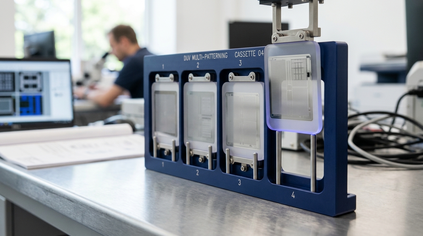
Figure 2. Multiple patterning buys pitch with process steps rather than aperture — a fourth mask, and everything that comes with printing, etching and measuring it again. — Image prompt and art direction by Brecht Corbeel; generation pending.
Given that arithmetic, multi-patterning is not a legacy technique waiting to be retired; it is the cheaper of two ways to buy pitch, and which one a fab chooses depends on the layer, the wafer volume that layer’s tool fleet needs to support, and how far along the high-numerical-aperture fleet’s own learning curve a given foundry sits. TSMC’s own technical description of its N3 generation states plainly that it moved 3-nanometre FinFET technology into high-volume production in 2022, describing N3 as “the industry’s most advanced FinFET technology” without reference to gate-all-around at that node [11] — a generation built, by construction, on the deep-ultraviolet and lower-numerical-aperture EUV patterning schemes that predate high-numerical-aperture tools entirely. The roadmap’s own expectation is that this coexistence continues rather than resolves: “as logic dimensions continue to shrink, use of EUV double patterning is likely” even as single-exposure high-numerical-aperture tools enter production alongside it [3]. imec’s own single-exposure demonstrations illustrate what the alternative looks like once it works: in September 2025 the lab reported 20-nanometre pitch line structures with 13-nanometre tip-to-tip critical dimensions and local critical-dimension uniformity as low as 3 nanometres using a metal-oxide resist, alongside a separate direct-metal-etch process printing ruthenium lines at 20- and 18-nanometre pitch with a reported 100 percent electrical test yield on the 20-nanometre pitch structures [5]. Those are results on imec’s own research test structures, not a foundry’s high-volume manufacturing yield, and the distinction matters enormously for how much weight the number should carry — but they are the clearest public evidence that single-exposure printing at these pitches is becoming a demonstrated capability rather than only a roadmap slide.
FinFET’s geometry runs out, and what wrapping the gate buys
The transistor-architecture axis runs on a more purely physical argument than the lithography one, though it is not independent of it. A FinFET’s gate wraps three sides of a vertical silicon fin — the top and both sidewalls — leaving the base of the fin outside the gate’s electrostatic control. As fins get taller and narrower to keep pace with density scaling, that uncontrolled base becomes a growing source of leakage and a growing obstacle to further shrinking. A gate-all-around transistor removes the asymmetry by laying the channel on its side as one or more thin horizontal sheets and wrapping the gate material completely around each one — top, bottom, and both sides.
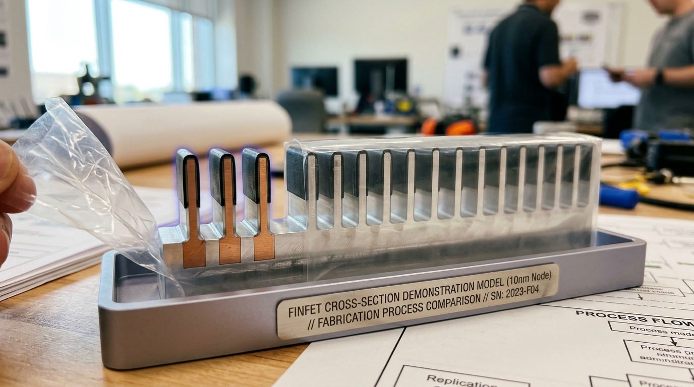
Figure 3. The fin is gated on three sides; the fourth, its base, stays outside the gate's control — the geometry the next comparison in this article turns on. — Image prompt and art direction by Brecht Corbeel; generation pending.
The paper that first demonstrated this at a competitive geometry, published jointly by IBM Research, Samsung Electronics, and GLOBALFOUNDRIES under their research alliance, is explicit that the motivation was electrostatic and the payoff was measured, not assumed. Loubet and colleagues reported that a single wide nanosheet stack could deliver up to a 30 percent increase in effective channel width at matched footprint compared with an aggressively scaled FinFET, and that single-stack nanosheet devices showed superior intrinsic performance across sheet widths because of reduced parasitic capacitance for a given active width — a better ratio of effective drive current to effective capacitance than either FinFET or a stacked-nanowire alternative [1]. They also made a point that connects directly back to the lithography axis: because a nanosheet’s width is a continuously variable lithographic parameter rather than a count of discrete fins, a single-exposure lithography step can fine-tune it for power or performance on a given design, where “FinFET and stacked Nanowire offer only crude granularity of one or two fins/stacks” [1]. On the manufacturing side, the same paper reported that the process required only a few specific divergences from an existing FinFET flow — multilayer channel epitaxy to grow the stacked sheets, a new inner-spacer formation step, a channel-release etch, and revised multi-threshold-voltage processing — rather than a wholesale reinvention of the front end.
Where the disagreement is real: a dissent worth taking seriously
The industry’s near-unanimous move toward gate-all-around architectures — Samsung first, TSMC and Intel since — can read as though the underlying physics settled the question outright. A 2022 peer-reviewed analysis by Wong and Kakushima, published in Nanomaterials, is worth taking seriously precisely because it complicates that reading without contradicting the underlying measurements. Working through the geometry under matched footprint and matched device height, the authors found that a vertically stacked nanosheet transistor only outperforms a FinFET once the vertical spacing between sheets falls below the sheet’s own width — a condition that, given present fabrication limits, requires spacing on the order of 7 to 8 nanometres, achievable only once fin widths below roughly 8 nanometres are reliably patternable [2]. Their reading of nanowire architectures is more pessimistic still: a comparable advantage there requires wire-to-wire spacing below 57 percent of the wire’s diameter, which they judge unrealistic with current gate-dielectric technology. They also point to a separate physical penalty that scales in the architecture’s favor at first and then works against it: channel mobility degrades from surface-roughness scattering as sheets and wires get thinner, worsening below roughly 10 nanometres in ways that erode some of the electrostatic gain gate-all-around is chosen for in the first place [2].
The conclusion Wong and Kakushima draw from this is genuinely at odds with the industry’s revealed preference, not merely more cautious about it: under conditions achievable with present fabrication technology, they argue, FinFET remains the stronger architecture at the most advanced nodes, and they characterise nanosheet adoption as best suited to fabs that cannot yet pattern narrow enough fins rather than as an unconditional advance [2]. This is not a fringe claim dressed up as one — it is a quantitative geometric argument published in a peer-reviewed materials-science journal, and it does not depend on disputing any of the measured results in the Loubet paper; it depends on which spacing and mobility regime a given foundry’s process can actually achieve, which is exactly the kind of implementation detail that does not appear on a roadmap slide. What can honestly be said is that three of the industry’s most resourced foundries made large, expensive, multi-year commitments to gate-all-around architectures despite this dissent being in the public literature, which is itself evidence about where those foundries believe their own process capability sits relative to the spacing threshold the paper identifies — but it is evidence about corporate confidence, not a refutation of the argument. Readers who see gate-all-around presented as a settled physical upgrade over FinFET should know that a peer-reviewed, quantitative counter-argument exists, and that resolving it requires foundry-specific process data that is not public.
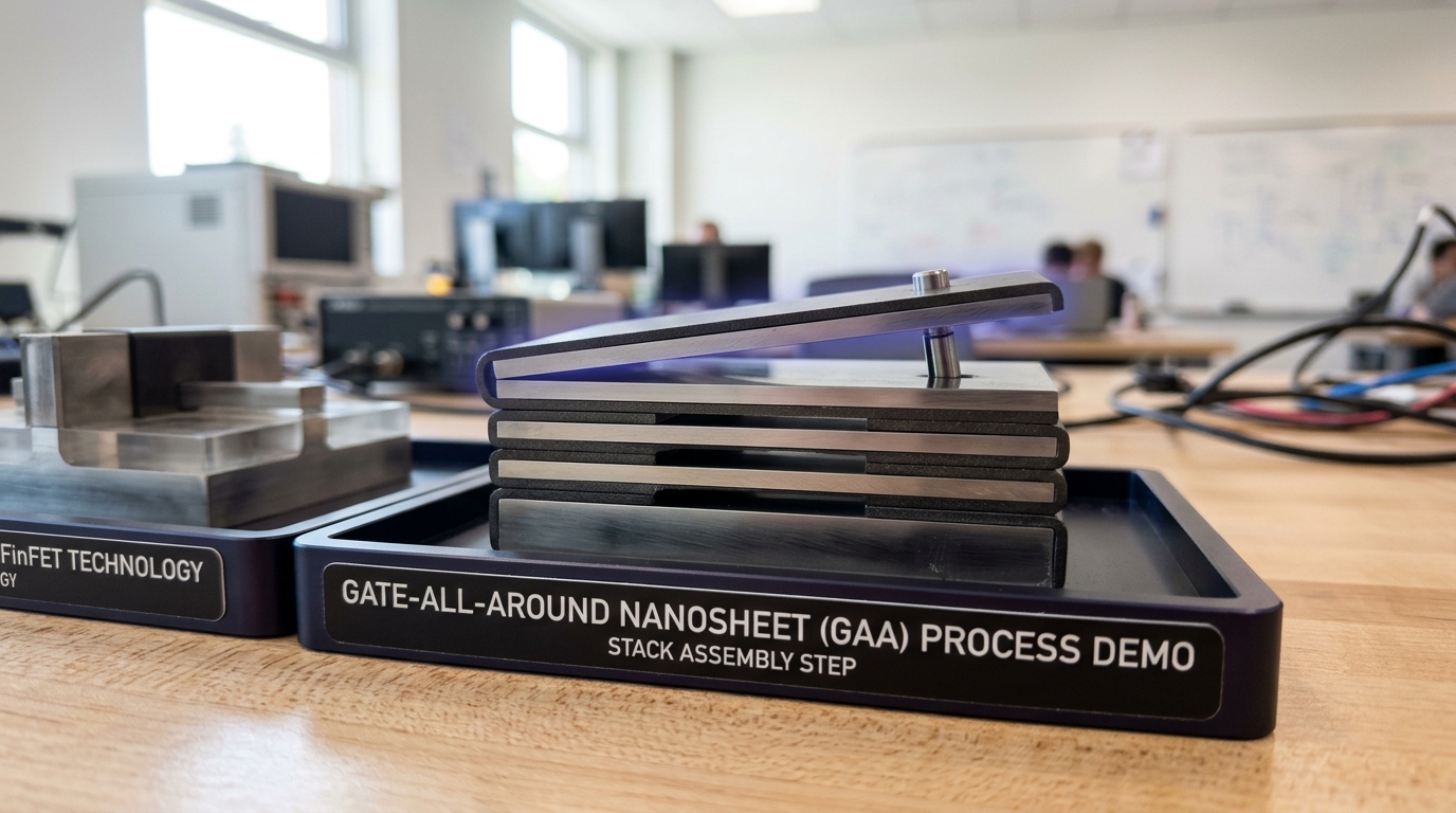
Figure 4. Whether the wrap-around gate is worth its cost depends on the exact spacing achieved between sheets — a condition, not a guarantee, and one qualified researchers read differently. — Image prompt and art direction by Brecht Corbeel; generation pending.
Three foundries, three sequencing decisions
Given a shared menu of two lithography strategies and two transistor architectures, TSMC, Samsung, and Intel chose to sequence and bundle them differently, and the differences are informative about each company’s risk appetite rather than about which company is “ahead.”
Samsung moved first and moved earliest into the harder architecture. Samsung’s own 2022 announcement states that it began initial production of a 3-nanometre process using gate-all-around transistors, which it brands MBCFET, describing first-generation gains against its own 5-nanometre FinFET node of 45 percent reduced power consumption, 23 percent improved performance, and 16 percent smaller area, with a stated target for a second generation of up to 50 percent power reduction, 30 percent performance improvement, and 35 percent area reduction [12]. These are Samsung’s own comparisons against its own prior node, not independently measured or comparable to a competitor’s claims on a different node, and they should be read as a vendor’s account of its own generational improvement rather than as a cross-company benchmark. Samsung’s bet was to absorb the manufacturing risk of a new transistor geometry two full node generations before its largest competitor did the same.
TSMC took the opposite sequencing. Its N3 generation, which entered high-volume production in the same year as Samsung’s first gate-all-around node, stayed on FinFET, and TSMC’s own technical description brands N3 as its most advanced FinFET technology rather than framing the choice as a delay [11]. TSMC held gate-all-around back for its N2 generation; IEEE Spectrum’s account of that transition, drawing on TSMC’s own technology symposium disclosures, describes more than four years of development work behind N2’s move to nanosheet transistors, with TSMC claiming up to 15 percent higher speed or up to 30 percent better energy efficiency and 15 percent higher density than N3, alongside a reported SRAM bit-cell density of 38 megabits per square millimetre — an 11 percent density gain that reverses several prior generations in which SRAM density improvements had been shrinking, N3’s own gain over its predecessor having been only about 6 percent [9]. TSMC’s sequencing bet was the reverse of Samsung’s: extend the mature, well-understood architecture as far as it would go, and adopt the new one only once its own process capability had matured elsewhere.
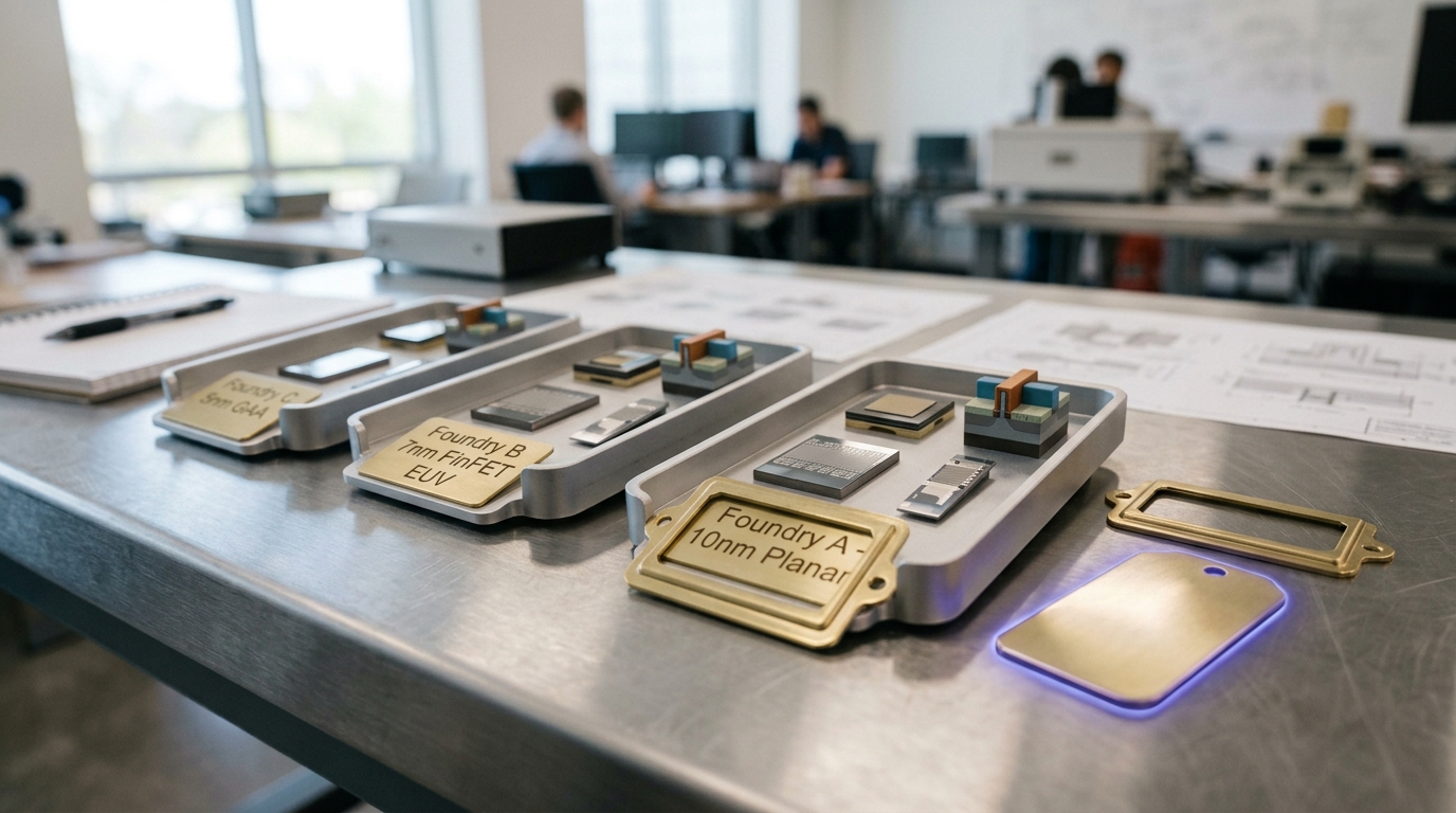
Figure 5. Three foundries reached the same destination by different routes and in a different order — a fact about sequencing, not a scoreboard. — Image prompt and art direction by Brecht Corbeel; generation pending.
Intel took a third path, bundling its gate-all-around transition together with an unrelated architectural change rather than staggering them. Intel’s backside power delivery scheme, which routes power wiring beneath the transistor layer instead of above it, was validated on an early test chip that Intel described as achieving over 90 percent cell utilisation, more than a 30 percent improvement in platform voltage droop, and a 6 percent frequency benefit, with the company stating it was first in the industry to demonstrate the technique on a product-like test vehicle and planning to introduce it alongside its next process generation [13]. Bundling a new power-delivery architecture with a new transistor architecture in the same generation concentrates manufacturing risk rather than spreading it across successive nodes, which is a legible bet about how much simultaneous change a single qualification cycle can absorb — the opposite instinct from TSMC’s staggered sequencing and a different kind of aggression from Samsung’s early single-axis bet on the transistor alone. None of the three sequencing choices is verifiably the “correct” one from public information; each is a defensible answer to a different risk-tolerance question, and the record so far shows all three companies still executing their respective bets rather than one having conclusively won.
Notably, gate-all-around is not where any of the three foundries stopped looking. At the December 2023 IEEE International Electron Devices Meeting, Intel, Samsung, and TSMC all separately demonstrated complementary field-effect transistors, which stack an n-type and p-type device vertically rather than side by side. Intel reached a 60-nanometre contacted poly pitch with three stacked nanosheets per device, up from two, and an Intel engineer described the ultimate scaling target as roughly half the area of a conventional side-by-side layout; Samsung reached 48- and 45-nanometre pitches and reported an 80 percent yield improvement on its test vehicle after replacing a wet chemical etch with a dry etch to isolate source and drain regions; TSMC reached an industrially relevant 48-nanometre pitch using a novel high-germanium-content dielectric formation, and the article covering the session estimates commercial deployment is seven to ten years out [10]. Samsung’s reported yield figure is worth flagging precisely because it is easy to misread: it describes a relative improvement on one integration step of a research test vehicle, not a production wafer yield — a useful illustration of how much of the real engineering risk in a new architecture lives in unglamorous steps like an etch chemistry choice rather than in the headline geometry.
What the yield numbers do and do not tell you
Public reporting on leading-edge yield is unusually noisy, and this comparison would be dishonest if it treated analyst rumors with the same weight as a foundry’s own disclosure. TrendForce reported in April 2026, citing unnamed industry sources via Korean press, that Samsung’s 2-nanometre-class yield sat in the mid-50 percent range — below what the report described as the roughly 60 percent threshold typically associated with stable mass production — against a reported 60 to 70 percent range at TSMC’s competing 2-nanometre node [14]. The report is explicit about its own evidentiary status, attributing the figures to unnamed sources rather than to either company’s own disclosure, and neither Samsung nor TSMC publishes wafer yield figures as a matter of course. Treat a number like this as a data point about market sentiment and analyst triangulation, not as a verified production metric, and be equally skeptical of any comparison — including ones favorable to either company — built on the same kind of sourcing.
What is independently corroborated, because it comes from the companies’ own architectural descriptions rather than from yield rumors, is the shape of the risk each foundry took on. A foundry adopting a new transistor architecture earlier than its competitors is, by construction, further out on its own learning curve at any given calendar date, and a foundry bundling two new architectural changes into one generation concentrates the number of things that must simultaneously work. Those structural facts do not resolve to a yield number, and this article will not manufacture one by averaging together reports of differing reliability. Yield risk differs across the three companies’ chosen sequencing in a direction predictable from the architectural bets already described; the specific magnitude is not something the public record currently supports comparing with precision.
The economics underneath the roadmap
Every choice described above compounds into a capital-intensity consequence worth stating plainly rather than leaving implicit. Single-exposure high-numerical-aperture lithography and extended multi-patterning are not a cheap option and an expensive one; they are two different capital commitments, and SEMI’s forecasting suggests the whole industry is absorbing both simultaneously, with worldwide 300-millimetre fab equipment spending projected to grow from 133 billion dollars in 2026 to 151 billion dollars in 2027 and Logic and Micro spending alone reaching roughly 228 billion dollars across 2027 through 2029, driven explicitly by sub-2-nanometre capacity additions [15].
This is also where comparing foundries becomes genuinely difficult to do fairly, and where this article declines to force one. TSMC, Samsung, and Intel do not disclose comparable per-node capital expenditure, comparable defect-density figures, or comparable yield curves, and the analyst estimates that fill that gap are built on different assumptions, different customer sets, and different degrees of access to any given company. A reader who wants a single number ranking the three companies’ cost efficiency will not find a responsible one in the public record as it stands, and any article that supplies one is manufacturing false precision rather than reporting it.
Geographic concentration is a fourth axis, not a footnote
The three engineering axes above do not fully describe the comparison, because where a fab sits is itself a variable that interacts with all three. TrendForce’s May 2024 capacity analysis put Taiwan’s share of global advanced-process foundry capacity at 66 percent as of that year, against 11 percent for South Korea, 10 percent for the United States, and 9 percent for China, and projected Taiwan’s share falling to 55 percent by 2027 while South Korea’s fell further to 8 percent and the United States’ share rose to 22 percent [18]. Those are forecasts built on announced fab construction and policy incentives rather than certainties, and TrendForce’s own report frames them as projections subject to revision as individual projects slip or accelerate.
The Semiconductor Industry Association and Boston Consulting Group’s 2024 supply-chain report, as reported by Power Semiconductors Weekly, reaches a directionally similar conclusion from a different angle: it projects the United States growing its share of global advanced-logic manufacturing capacity below 10 nanometres from zero percent in 2022 to 28 percent by 2032, with Taiwan remaining the largest single destination for the roughly 2.3 trillion dollars in projected industry capital expenditure across 2024 through 2032 at an estimated 31 percent share [17]. Both figures describe the same dynamic from different vantage points: subsidy-driven capacity building elsewhere is real and already under construction, but it is redistributing a growing pie rather than displacing Taiwan’s central position in the near term, and the two companies furthest along the gate-all-around and high-numerical-aperture transitions — TSMC and Samsung — remain concentrated in Taiwan and South Korea respectively.
Reading rules for anyone comparing these approaches
Four rules follow directly from working through the axes above, and they are the practical content of everything in this piece.
Separate the lithography axis from the transistor axis before comparing anything. A foundry’s choice of single-exposure or multi-pass patterning and its choice of fin or gate-all-around architecture are independent decisions with independent cost structures; collapsing both into “how advanced” a node is destroys the information a real comparison needs.
Attribute every percentage to its source and its baseline. A vendor’s own generation-over-generation claim, an analyst’s yield estimate sourced to unnamed contacts, and a peer-reviewed geometric result are three different kinds of evidence with three different failure modes, and none of them should borrow the others’ credibility by appearing in the same sentence unlabelled.
Treat unconfirmed yield figures as sentiment, not measurement. No major foundry publishes wafer-level yield data as a matter of routine disclosure; a specific percentage attributed to “industry sources” is a data point about what analysts currently believe, not a verified fact about a production line.
Do not build a ranking from figures that were not measured under the same conditions. Samsung’s claims are against its own prior node; TSMC’s are against its own prior node; Intel’s test-chip results describe a specific test vehicle. None of the three is stated on a common baseline, and forcing them onto one manufactures a comparison the source data does not support.
Predictions, with what would falsify them
These are forecasts, kept separate from the sourced analysis above. Horizon: 15 August 2029. Assumptions: no fabrication approach outside projection lithography and gate-all-around-family transistors reaches high-volume manufacturing within the window, and no single foundry suffers a process-qualification failure severe enough to force a return to a prior node.
One. High-numerical-aperture EUV and DUV multi-patterning will continue to coexist on the same foundries’ leading-edge process flows rather than one displacing the other, with the choice made layer by layer along the lines the 2023 IRDS roadmap already describes. Disconfirmed if a leading foundry publicly ships a node on which every critical layer uses single-exposure lithography with no multi-patterning anywhere in the flow.
Two. Complementary field-effect transistors will not reach high-volume manufacturing within this horizon; gate-all-around and its direct refinements will remain the production architecture through at least one more full node generation at each of the three foundries discussed here. Disconfirmed if any of the three ships a CFET-based node in high-volume production before August 2029.
Three. Public, unattributed yield figures for leading-edge nodes will remain the primary source of cross-foundry yield comparison, because none of the three companies will begin routinely disclosing production yield data. Disconfirmed if TSMC, Samsung, or Intel begins publishing node-level yield figures as a standard part of quarterly disclosure.
Four. Geographic capacity share will shift gradually in the direction TrendForce and the SIA/BCG report both project, without Taiwan losing its position as the largest single concentration of advanced-node capacity within this window. Disconfirmed if published capacity data shows Taiwan’s share of advanced-process foundry capacity falling below the United States’ or South Korea’s individual shares before 2029.
None of these requires a surprise. They follow from the structure already documented: two genuinely different lithography economics that solve different layers’ problems, a transistor-architecture consensus that coexists with a real published dissent about the conditions under which it holds, three foundries executing three different risk sequences none of which has been falsified yet, and a capacity map that is diversifying without yet being displaced.
What to take away
There is no single ranking hiding underneath “advanced semiconductor fabrication” waiting to be revealed once enough numbers are gathered. There are two different ways to print a pattern, each cheaper under different conditions; two different transistor geometries, one of which the industry has bet on despite a serious peer-reviewed argument that the bet is conditional rather than settled; and three foundries that read the same menu of choices and ordered from it differently, for reasons that look like defensible risk management rather than error, on either side. The vendor claims in this comparison are vendor claims, the analyst estimates are analyst estimates, and the one peer-reviewed dissent about gate-all-around’s advantages deserves to be read as seriously as the roadmap consensus it complicates. Anyone who reduces this landscape to “Company X is ahead” has already discarded the information that made the comparison worth making.
Sources
- N. Loubet, T. Hook, P. Montanini, et al. (IBM Research, Samsung Electronics, and GLOBALFOUNDRIES Research Alliance). Stacked Nanosheet Gate-All-Around Transistor to Enable Scaling Beyond FinFET. 2017 Symposium on VLSI Technology Digest of Technical Papers (2017).
- Hei Wong and Kuniyuki Kakushima. On the Vertically Stacked Gate-All-Around Nanosheet and Nanowire Transistor Scaling beyond the 5 nm Technology Node. Nanomaterials (2022). DOI: 10.3390/nano12101739.
- IEEE IRDS Lithography and Patterning International Focus Team. International Roadmap for Devices and Systems 2023 Update: Lithography and Patterning. IEEE (2023).
- imec. The case for High NA EUV: unlocking the next era of chip manufacturing. imec (2026).
- imec. Imec achieves new milestones in single patterning High NA EUV lithography for both damascene and direct metal etch metallization processes. imec (2025).
- ASML. TWINSCAN EXE:5000. ASML (2026).
- ASML. 5 things you should know about High NA EUV lithography. ASML (2024).
- Tom's Hardware Staff. ASML's High-NA chipmaking tool will cost $380 million — the company already has orders for '10 to 20' machines and is ramping up production. Tom's Hardware (2024).
- Samuel K. Moore. TSMC Lifts the Curtain on Nanosheet Transistors. IEEE Spectrum (2024).
- Samuel K. Moore. Intel, Samsung, and TSMC Demo 3D-Stacked Transistors. IEEE Spectrum (2023).
- TSMC. 3nm Technology. Taiwan Semiconductor Manufacturing Company (2026).
- Samsung Electronics. Samsung Begins Chip Production Using 3nm Process Technology With GAA Architecture. Samsung Semiconductor Global (2022).
- Intel Corporation. PowerVia Test Shows Industry-Leading Performance. Intel Corporation (Business Wire) (2023).
- TrendForce. Samsung 2nm Yields Reportedly at ~55%, Below Mass Production Threshold; Qualcomm May Opt for TSMC. TrendForce (2026).
- SEMI. SEMI Projects Double-Digit Growth in Global 300mm Fab Equipment Spending for 2026 and 2027. SEMI (distributed via PR Newswire) (2026).
- Erika Morphy. A 2nm-capable wafer fab will come with a $28 billion tag, up to 50% more costly than 3nm. TechSpot (2023).
- Power Semiconductors Weekly. SIA and BCG Publish Global Chip Supply Chain Report. Power Semiconductors Weekly (2024).
- TrendForce. [Insights] TrendForce: Foundry Capacity Market Share of Advanced Process to Decline in Taiwan, Korea until 2027, While US on the Rise. TrendForce (2024).
Originally published at https://absolutedigitalpublishers.com/articles/comparing-the-main-approaches-to-advanced-semiconductor-fabrication.