Chips Started Growing a Second Face to Survive Their Own Wiring
Intel fused gate-all-around transistors to backside power delivery on a node it then cancelled. TSMC and Samsung are repeating the same two moves a full node apart, on different clocks — a lag too consistent across foundries to be coincidence.
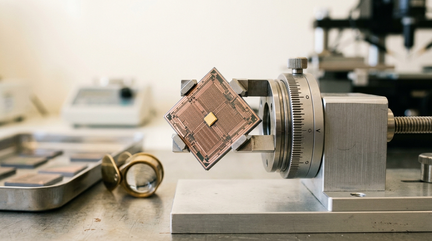
Nothing about this die changed shape. It was ground down from behind, polished, and etched until a second working face appeared where solid substrate used to be — the whole argument of this article compressed into one object mid-turn. — Image prompt and art direction by Brecht Corbeel; image generated to that direction.
Abstract
In September 2024, Intel cancelled the external commercial life of a manufacturing node, Intel 20A, that had already done something no chip had done before: pair a gate-all-around transistor with backside power delivery on the same die. The node's name died; the pairing did not — it shipped a year later as Intel 18A. This article tracks that pairing as its own engineering lineage, independent of the FinFET-to-GAA transistor story usually told about the same years, across Intel, TSMC, Samsung, and Rapidus's four separately disclosed timelines. Backside power delivery arrives after gate-all-around at every one of the four, including the one foundry with the least reason to inherit anyone else's caution, and the interval between the two varies from foundry to foundry without ever once running in the other direction — a pattern this article argues is a branch of its own, with its own maturity curve, not a line item bundled into whatever a foundry decides to call its next node.
In September 2024, Intel cancelled a manufacturing node for outside customers before it ever shipped a commercial chip [3]. Intel 20A was supposed to carry Arrow Lake, Intel’s next consumer processor generation, into production; instead, Arrow Lake’s silicon went to TSMC, and Intel said skipping 20A’s production ramp would save more than half a billion dollars in capital spending it no longer needed to make [4]. By the metric that usually matters in this industry — did it ship — Intel 20A was a failure. By the metric this article is built around, it was the opposite: 20A was where Intel first proved, on real silicon, that a gate-all-around transistor and a backside power delivery network could sit on the same die at the same time — Intel itself said it had “successfully implemented RibbonFET gate-all-around architecture and PowerVia backside power delivery” on 20A, work that then accelerated 18A’s own development [4]. The node’s commercial name died. What it proved did not. It shipped thirteen months later as Intel 18A, and the pairing it demonstrated first, internally, on a cancelled node, is the same pairing TSMC and Samsung are now assembling in public, on their own separate schedules, each a full node behind where they put the transistor architecture alone.
That is the claim this article tracks: backside power delivery is not a line item inside the FinFET-to-gate-all-around transition usually used to explain “the move to 2nm.” It is a second, independently timed engineering transition, running behind the first one by an interval that differs at every foundry but that never once runs the other way. Nobody has shipped backside power delivery ahead of gate-all-around, and nobody besides Intel has committed to shipping the two together — every other foundry, including the one with the least legacy to protect, plans to ship gate-all-around first and add backside power afterward. The lag itself, not any single foundry’s percentage figures, is the finding.
Intel Proved the Pairing, Then Un-Proved It Commercially
Intel’s own account of Intel 18A describes it as pairing “RibbonFET,” Intel’s implementation of a gate-all-around transistor, with “industry-first” backside power delivery, called PowerVia, inside one production-ready process built for high-volume manufacturing [5]. That combination first ran, in silicon, on Intel 20A — the node cancelled for Arrow Lake — before it became a headline feature of 18A [4]. Intel 18A itself is now in high-volume manufacturing, per Intel’s own current disclosure, though the company’s public materials state that status without naming the specific quarter it began [5], and it underpins Panther Lake, the first Intel Core Ultra Series 3 processor built on it. Intel’s own current figures for 18A against its immediate FinFET-era predecessor, Intel 3, state up to 18 percent higher performance at the same power draw, up to 38 percent lower power at matched performance, and more than 30 percent higher transistor density [5]. A separate, more granular figure from the same disclosure — a 25 percent frequency gain, reported specifically at a fixed 1.1-volt operating point — is not a second reading of that same 18 percent number: one is an iso-power performance comparison, the other an iso-voltage frequency comparison, and neither Intel’s materials nor the secondary reporting on them collapses the two into one figure [6]. Those numbers describe the whole node, transistor architecture and power delivery together, because Intel has never shipped a 2-nanometer-class commercial process with one of the two technologies and not the other. Every other foundry has.
That is worth sitting with for a moment, because it inverts the usual industry narrative about who is behind whom. Samsung reached gate-all-around production first, in June 2022 — three years ahead of Intel — and TSMC reached its own first gate-all-around node, N2, in the fourth quarter of 2025 [7], after years of being described as the industry’s pacesetter. On the specific, narrower question this article asks — has your foundry ever put a gate-all-around transistor into commercial production without backside power delivery attached to it — Intel is the only one of the three that can answer no, and the answer is no only because a cancelled node absorbed the risk of doing both at once before either technology touched a paying customer’s silicon.
The Wire Problem Gate-All-Around Does Nothing to Solve
Every one of a chip’s transistors needs two separate things routed to it: a signal telling it what to do, and power to do it with. For decades, both traveled through the same stack of metal wiring layers on the front of the wafer, built up on top of the transistors after they were etched. As that front-side stack has had to carry more current through steadily thinner, steadily more resistance-prone wires, the voltage a transistor actually receives has started measurably sagging below the voltage a chip’s designer specified — a problem circuit designers call IR drop, and one that gets worse, not better, every time transistors are packed more densely into the same wiring budget. Gate-all-around transistors do not touch this problem at all. A gate-all-around transistor is a fix to a different, earlier-stage failure: at very short gate lengths, a FinFET’s imperfect grip on the channel starts leaking current the transistor is supposed to be blocking, and wrapping the gate fully around the channel restores control. That is a transistor-body fix. It says nothing about how power reaches the transistor once it has been built, which is exactly why a foundry can adopt gate-all-around and still be delivering power the old way, front-side, through the same congested stack — as Samsung, TSMC, and Rapidus have each done, or are each currently doing, at their first gate-all-around nodes.
The reason the two problems get worse on the same schedule without being the same problem is simple enough to state without a citation: a wire’s resistance is its resistivity times its length divided by its cross-sectional area, and every node shrink cuts that cross-section again while the total current a chip draws keeps climbing, not falling, because there are more transistors switching inside the same die footprint. Voltage drop is current times resistance, so a wire carrying more current through a smaller cross-section drops more voltage across its own length, independent of anything happening inside the transistor sitting at the far end of it. A gate-all-around transistor can be electrostatically perfect and still receive a supply voltage that has sagged below what its designer specified, because the sag happened in the metal on the way there, not in the channel. That is the derivation underneath this article’s central separation: the transistor-body problem and the wiring problem scale on the same rough timeline, at the same rough node cadence, because both are downstream of the same shrink — but scaling on the same timeline is not the same claim as being the same mechanism, and only one of the two problems is fixed by changing the transistor.
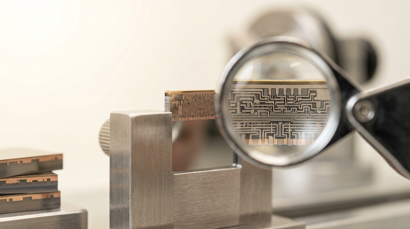
Figure 1. Every one of these layers has to carry either a signal or a share of the chip's power. Gate-all-around transistors do nothing to widen this stack — the congestion here is a wiring problem, not a transistor problem. — Image prompt and art direction by Brecht Corbeel; image generated to that direction.
The fix for the wiring problem specifically — move power delivery to the wafer’s back side, freeing the entire front-side stack for signal routing alone — was not invented by a foundry preparing a product announcement. Arm’s device-research group and imec published the mechanism in December 2019, five years before any commercial foundry shipped it: a design using a rail buried directly beneath the transistor layer, connected down to the wafer’s reverse side through miniature through-silicon vias, delivering power from underneath rather than routing it down from above [2]. Their reported result was not a marginal improvement. Front-side power delivery alone left the test design with a substantial voltage drop under load; adding the buried-rail-to-backside connection improved that voltage drop by up to 90 percent, bringing it down to roughly one percent, without giving up performance elsewhere on the chip [2]. That is a five-year-old, publicly disclosed research result, running on a completely different clock than the FinFET-to-gate-all-around transition that occupied foundry roadmaps across the same years. Nothing about it required gate-all-around to exist first. It could, in principle, have shipped on a FinFET node. It did not, because the industry treated it as a separate problem worth solving on its own timeline — which is precisely the claim this article is making about the years since.

Figure 2. Five years before any foundry shipped backside power, Arm and imec had already built this: a rail buried beneath the transistor and wired down to the wafer's reverse side. The mechanism was proven long before it was product. — Image prompt and art direction by Brecht Corbeel; image generated to that direction.
TSMC Split the Two Transitions a Full Node Apart, on Purpose
TSMC’s N2 process, its first implementation of gate-all-around nanosheet transistors, entered volume production in the fourth quarter of 2025 at Fab 22 near Kaohsiung, “as planned” — TSMC’s own characterization of hitting a date it had set years earlier [7]. N2 carries no backside power delivery. Against N3E, its immediate FinFET-era predecessor, TSMC states a 10-to-15-percent performance gain at matched power, a 25-to-30-percent power reduction at matched performance, and a density increase of roughly 15 percent for mixed logic-and-SRAM designs, rising to as much as 20 percent for logic-only blocks [7]. Backside power delivery arrives a full node later, on A16, under the name Super Power Rail. As of August 20, 2026 — three weeks before this article was drafted — TSMC had completed development and verification of A16, with mass production still scheduled for the fourth quarter of 2026, on the same timeline the company set publicly in November 2024 [9, 8]. Measured against N2P, N2’s own refined successor, A16 is expected to deliver an 8-to-10-percent performance gain at matched voltage and design complexity, a 15-to-20-percent power reduction at matched frequency and transistor count, and a density increase of roughly 7 to 10 percent [8, 9].
That is a one-year gap, computed directly from two dates TSMC itself has published and, as of August 2026, has not moved: gate-all-around alone in Q4 2025, gate-all-around with backside power a year later in Q4 2026. TSMC did not lack the capability to combine the two at N2 — imec and Arm had already shown the mechanism worked five years earlier. TSMC chose to phase the risk, shipping one new manufacturing variable at a time rather than validating a transistor architecture and a power-delivery architecture simultaneously on the same production line. That is a deliberate sequencing decision, not a sign the second technology was unready in some absolute sense; it is a foundry choosing, in public, to treat the two as separable enough to schedule separately.
Samsung Is Repeating the Same Two Steps, on a Slower Clock
Samsung reached the first half of this sequence earliest of any foundry. On June 30, 2022, Samsung announced it had begun production on its 3-nanometer process, 3GAE, using what Samsung calls Multi-Bridge-Channel Field-Effect Transistors — its own gate-all-around implementation — describing the milestone as the industry’s first commercial use of gate-all-around transistor architecture [1]. That node carried no backside power delivery. Samsung’s own disclosed second half of the sequence, a backside power delivery network for its 2-nanometer-class SF2Z process, is targeted for 2027, still the standing date as of Samsung’s most recently reported roadmap [11]. Lee Sungjae, vice president of Samsung Foundry’s PDK Development Team, put specific numbers to that transition in 2024: a 17 percent reduction in 2-nanometer chip size, alongside an 8 percent performance gain and a 15 percent power-efficiency improvement, all measured against Samsung’s non-backside-power 2-nanometer baseline [10]. Industry analysis covering all three foundries’ backside-power timelines together places Samsung’s SF2Z roughly two years behind Samsung’s own 2-nanometer-generation gate-all-around rollout — a longer internal gap than TSMC’s one year, running on Samsung’s own separate clock [12].
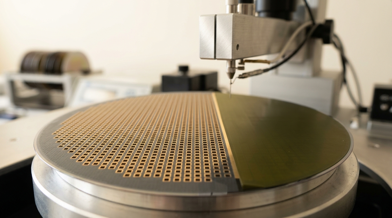
Figure 3. This is the part no press release photographs: to reach the transistor from underneath, almost the entire wafer has to be removed first. What is left is a few micrometres thick before a single via is opened. — Image prompt and art direction by Brecht Corbeel; image generated to that direction.
The Lag Is Consistent in Direction, Never in Length
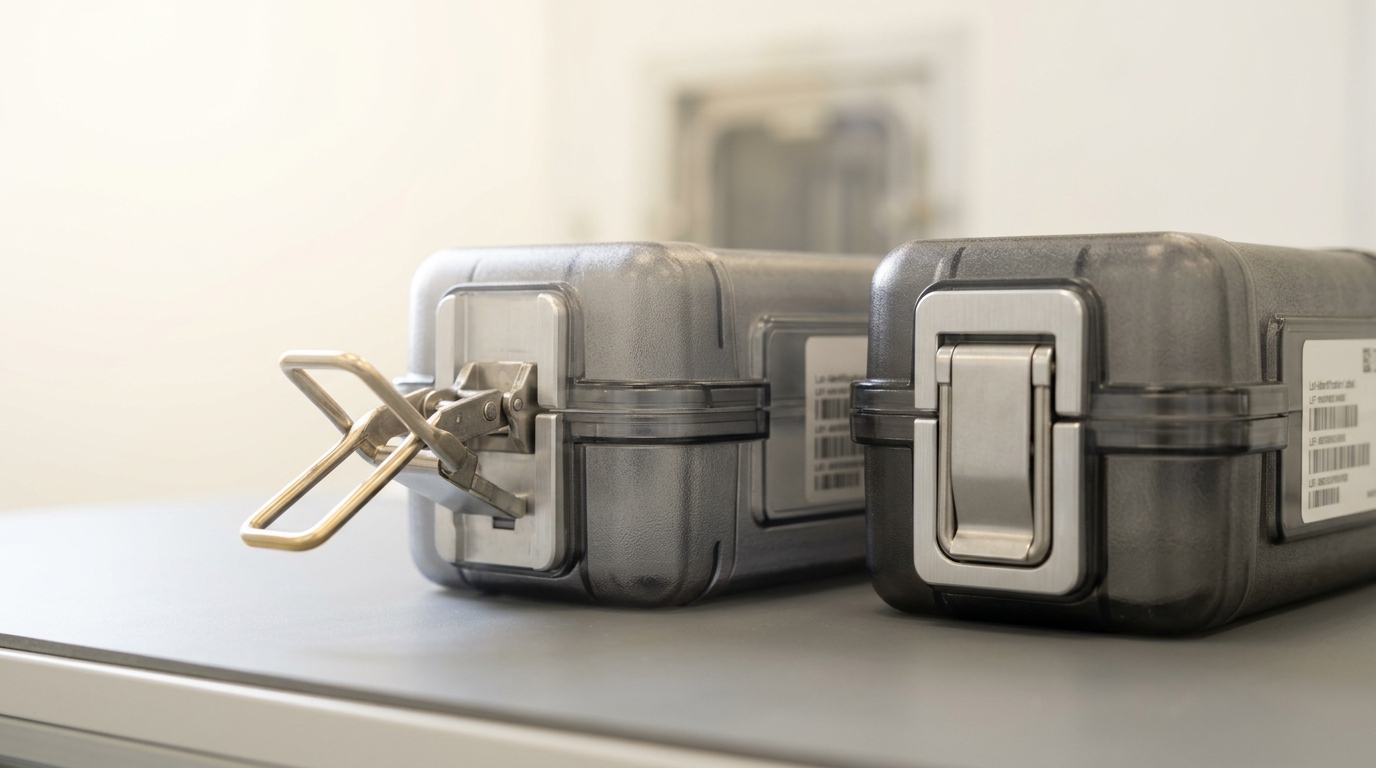
Figure 4. One of these lots is finished and sealed. The other is not — and the gap between them is not a delay or a failure, it is the actual shape of how backside power has moved through this industry: after gate-all-around, never before it, by an interval nobody had to coordinate. — Image prompt and art direction by Brecht Corbeel; image generated to that direction.
Line the four foundries up by their own published dates and the shape is consistent even though the length is not:
- Foundry — Gate-all-around alone — Gate-all-around + backside power — Computed gap
- Intel — Never shipped commercially without it — 18A, currently in high-volume manufacturing, exact quarter undated in Intel’s own materials [5] — ~0 — combined by first commercial shipment, after absorbing the risk on cancelled node 20A [4]
- TSMC — N2, volume production Q4 2025 [7] — A16, mass production targeted Q4 2026 [9] — ~1 year
- Samsung — 3GAE, production began June 2022 [1] — SF2Z, targeted 2027 [11] — ~2 years at the 2nm generation specifically [12]
- Rapidus — 2nm pilot line, April 2025; HVM targeted 2027 [13] — BSPDN to follow “shortly after” the 2027 HVM start, per Rapidus Design Solutions president Henri Richard [13] — Shortest of the four — an immediate follow-on rather than a dated multi-year wait
Two caveats belong directly beside that table rather than buried in a footnote. Samsung’s row measures the gap at the 2-nanometer generation specifically, where SemiAnalysis’s own comparative framing places it, not from 3GAE’s 2022 date — 3GAE and SF2Z are different node generations three years and one full transistor-density class apart, and treating the raw calendar distance between them as “Samsung’s lag” would overstate the number by conflating two separate node transitions. And Rapidus’s gap is reported here as the shortest of the four rather than as a number of years, because the only figure its own executive has put on it is relative rather than dated: Henri Richard, president of Rapidus Design Solutions, has said Rapidus’s backside power delivery network “will be provided shortly after the start of our mass production in 2027” [13] — a real, named commitment, just not one pinned to a calendar year the way TSMC’s and Samsung’s targets are.
With those caveats stated, the direction is what survives scrutiny: zero foundries reached backside power delivery before gate-all-around, and only one — Intel — reached them simultaneously in a commercial shipment, and did so by paying the combination’s schedule risk down separately, in private, on a node it ultimately discarded. That ordering, repeated by four organizations with four different balance sheets, four different customer bases, and four different incentives to move faster or slower than their rivals, is not the kind of thing that happens by coincidence of shared engineering difficulty alone. It is what a genuinely separate branch of the technology tree looks like when several organizations climb it independently and arrive, each on its own clock, at the same order of operations.
A Fourth Data Point: The Foundry With the Least Reason to Wait, Waiting Anyway
Rapidus, Japan’s state-backed foundry venture, opened a 2-nanometer pilot line at its integrated facility in Chitose, Hokkaido, in April 2025, using a gate-all-around process co-developed with IBM, with high-volume manufacturing targeted for 2027 [13]. Backside power delivery is not part of that first 2027 offering — but it is not absent from the roadmap either. Henri Richard, president of Rapidus Design Solutions, has said the company’s backside power delivery network “will be provided shortly after the start of our mass production in 2027 and is an integral part of the roadmap going forward” [13]. That is a real commitment from a named executive, just one described relative to a milestone rather than pinned to a calendar year the way TSMC’s and Samsung’s targets are. It still makes Rapidus the fourth foundry to confirm the pattern, not an exception to it: gate-all-around ships first, backside power delivery follows, and the only thing unusual about Rapidus’s case is how short the stated interval is — “shortly after,” not a stated number of years, but after all the same, never before.
Rapidus is, of the four, the one with the least reason to inherit anyone else’s caution. It is not protecting an installed base of customers qualified on an older process, the way TSMC and Samsung both are; its 2-nanometer line, developed with IBM, is close to a clean-sheet build. If backside power delivery were mainly a legacy-integration problem — something hard chiefly because it has to coexist with decades of existing front-side-only design tooling and customer qualification processes — a fresh entrant with no such legacy would be the likeliest of the four to ship it simultaneously with gate-all-around, on day one, the way Intel eventually did. Rapidus instead does what every other foundry in this article does: ships the transistor architecture first and adds backside power afterward, even with none of TSMC’s or Samsung’s installed-base excuse available to it. That the one foundry freest to skip the sequencing still keeps it suggests the harder part is not legacy integration at all, but the wafer-thinning, backside-alignment, and yield discipline the technology itself demands regardless of who is building it — the same discipline Arm and imec’s 2019 demonstration proved was achievable on a test coupon, and that four production organizations are still working through, each at its own pace, six years later.
That reframing — treating backside power delivery as its own branch with its own adoption timeline, rather than as one bullet point inside whatever a foundry decides to call its next node — is not how any of the four companies describe their own roadmaps. Each presents it as one improvement among several in a bundled node-over-node comparison table. Separating it out into an independent lineage, tested against a consistent ordering across four organizations, is this article’s own move, and the case for it rests on nothing more exotic than lining up dates each company has already published and noticing that the order never inverts.
The Second Face Is Ground Down, Not Grown
The title of this article borrows a biological image on purpose, and that image incurs a debt worth paying immediately. What a chip getting backside power delivery actually undergoes maps, loosely, to growing a second face: a wafer is thinned from its original few-hundred-micrometre thickness down to a few micrometres of remaining substrate, then processed from that newly exposed reverse side to open contacts down to the transistor layer, and once that is done the chip genuinely does have two functional faces where it used to have one, each doing different work. That much of the metaphor holds. Where it breaks is in the direction of the process. Growing a face, in every sense biology gives the word, is additive: cells divide, tissue accumulates, structure emerges from material that was not there before. Manufacturing a chip’s backside is the exact opposite operation. Almost the entire original wafer thickness is removed — ground away and etched down until, in the case of the most aggressive backside-contact schemes, well under a hundred nanometres of original silicon substrate remains before a single via is opened from beneath. The “second face” is not new tissue laid down on top of what existed before. It is the old material stripped away until what was always the transistor layer’s underside becomes newly accessible, then wired up as if it were a second front. A chip does not grow a second face so much as it is excavated down to one. The metaphor earns its place in a title because the outcome — one die, two independently useful sides — really does resemble what it names; it fails, and should be understood to fail, as an account of the mechanism, which runs backward from what “growing” would suggest.
What Would Prove This Wrong
This article’s claim is falsifiable in a specific, near-term way, and stating the failure condition plainly is part of making the claim honestly. TSMC’s A16 and Samsung’s SF2Z are the two remaining live tests. TSMC has stated 8-to-10-percent performance, 15-to-20-percent power, and roughly 8-to-10-percent density gains for A16 against N2P, tied to a fourth-quarter-2026 mass-production date the company reaffirmed as recently as August 2026 [8, 9]. Samsung has stated 17 percent, 8 percent, and 15 percent figures for SF2Z against its non-backside 2-nanometer baseline, tied to a 2027 date [10, 11]. If either node ships and independent measurement finds its actual IR-drop or density benefit falling meaningfully short of these pre-announced figures — not a rounding difference, but a shortfall outside ordinary measurement uncertainty — then the claim in this article that backside power delivery is a distinct engineering branch delivering a genuine step-function benefit, rather than a marketing bundle of incremental gains dressed up as a discrete transition, would be falsified. The branch would still exist as a manufacturing fact; it would simply not be doing the work this article credits it with.
There is a second, longer-horizon way this framing could stop applying, and it belongs explicitly in a lower, more speculative register than anything above it, because no foundry has committed to it on any dated roadmap. CFET — a transistor architecture that stacks an n-type and a p-type device vertically in one footprint, currently at the imec-demonstration stage with no foundry production commitment as of this research pass — could, if it eventually arrives, fold power delivery into a genuinely three-dimensional interconnect fabric rather than treating “front” and “back” as the chip’s only two addressable faces. If that happens within the next two or three node generations after CFET’s eventual commercial debut, whenever that debut occurs, the front-side/backside distinction this entire article is built on could become a temporary, two-decade feature of chip manufacturing rather than a permanent one. That is speculation with no committed date attached to it anywhere in the industry today, offered here only as the honest boundary of how far this article’s branch-lineage claim should be trusted to extend.
Every Foundry Is Running Two Independent Clocks, Not One
The practical upshot is narrower than a grand statement about chip design, and more useful for exactly that reason. Every foundry examined here is really running two separately scheduled engineering programs at once, not one: a transistor-architecture clock that answers whether the process controls its channel well enough at a given gate length, and a power-delivery clock that answers whether the process gets power to that transistor without losing a meaningful fraction of it to resistance on the way in. Intel is the only one of the four running both clocks on the same tick, because Intel paid down the schedule risk of synchronizing them on a node, 20A, it was willing to discard commercially the moment the internal proof was banked. TSMC and Samsung have each set their transistor-architecture clock running with their power-delivery clock trailing it by a separately reaffirmed interval — one year at TSMC, roughly two at Samsung’s 2-nanometer generation specifically. Rapidus’s power-delivery clock trails by the shortest interval of the four, on its own executive’s word, but trails all the same. A chip inherits whatever position each of its foundry’s two clocks actually occupies on its ship date, not some average implied by a single process label — which means two chips built on nominally comparable processes can differ, in exactly the dimension that decides how much of a power budget survives the trip from package to transistor, by however many years separate their foundry’s two clocks from lining up.
A designer choosing between foundries for a power-constrained part — an accelerator, a mobile processor, anything where the last few percent of delivered voltage decides a clock speed bin — is choosing a point on two independent timelines at once, whether or not the choice gets framed that way, and the two timelines do not move together just because a single roadmap slide lists them under one process name. The same caution applies to reading this article’s own numbers forward: A16 and SF2Z are, as of today, announced figures on announced dates, not yet independently measured shipping silicon, which is exactly why the kill criterion above is stated in terms of what those two nodes actually deliver against their own pre-announced targets, rather than treated as settled in advance because a press release already used the percentages.
Sources
- Samsung Begins Chip Production Using 3nm Process Technology With GAA Architecture. Samsung Newsroom (2022).
- D. Prasad, S. T. Nibhanupudi, A. Spessot, and colleagues (Arm and imec). Buried Power Rails and Back-side Power Grids: Arm CPU Power Delivery Network Design Beyond 5nm. Arm Research (IEDM 2019) (2019).
- Intel's 18A Reportedly Runs into Trouble with Broadcom, while 20A Plan on Arrow Lake Cancelled. TrendForce (2024).
- Intel Announces Cancellation of 20A Process Node for Arrow Lake — Goes With External Nodes Instead, Likely TSMC. Tom's Hardware (2024).
- Intel 18A: See Our Biggest Process Innovation. Intel Foundry (2026).
- Intel 18A Process Node Offers 25% Higher Frequency At ISO & 36% Lower Power At Same Frequency Versus Intel 3, Over 30% Density. SemiWiki (2025).
- TSMC's 2nm N2 process officially enters volume production. TechSpot (2025).
- TSMC Is On Track for A16 Mass Production in Late 2026 with Advanced Backside Power Delivery. TrendForce (2024).
- Taiwan's TSMC Completes 1.6-nm Chip, Eyes Q4 Mass Production. Seoul Economic Daily (2026).
- Samsung's Backside Power Delivery Network Reportedly to Reduce 2nm Chip Size by 17%. TrendForce (2024).
- New Samsung 2nm roadmap shows backside power delivery coming in 2027. TechSpot (2026).
- Clash of the Foundries: Gate All Around + Backside Power at 2nm. SemiAnalysis (2024).
- Mark Lapedus. Japan's Rapidus Preps 2nm Foundry Process And Chiplets. Mark Lapedus (Substack) (2025).
Originally published at https://absolutedigitalpublishers.com/articles/chips-started-growing-a-second-face-to-survive-their-own-wiring.