Advanced Semiconductor Fabrication in 2035: Scenarios, Signals, and Falsifiable Predictions
High-NA EUV has already shipped in volume at one company while its rivals hesitate. CFET has a date attached to it. New fabs are rising outside Taiwan and Korea. This article states, for each 2035 trajectory, what would prove it wrong.
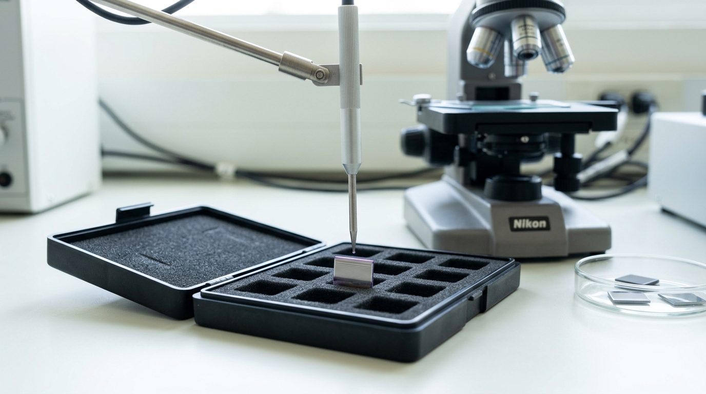
Every dated claim in this article eventually has to survive contact with a sample like this one — cut, but not yet even placed under a lens. — Image prompt and art direction by Brecht Corbeel; generation pending.
Abstract
This article builds five dated, falsifiable scenarios for where advanced semiconductor fabrication goes by 2035: whether High-NA EUV becomes a multi-vendor production workhorse or stays concentrated at one manufacturer; whether complementary FET (CFET) transistor stacking reaches volume production near imec's own stated 2033 date; whether new fab capacity in Arizona and Hokkaido diversifies who controls leading-edge logic or only where it is built; whether two-dimensional channel materials clear the materials-supply gap that independent literature still calls immature; and whether nanoimprint lithography, or anything else, is close to forcing a genuine patterning discontinuity. Each trajectory separates documented fact from vendor and institutional claim, from this article's own analysis, from the scenario branches consistent with the evidence, and from a specific prediction carrying a horizon, explicit assumptions, an observable indicator, and a stated disconfirmation condition. No trajectory is named as the likely one, and where the organisations building these tools visibly disagree, the disagreement is described rather than resolved.
Five clocks, not one forecast
Advanced fabrication does not have one 2035. It has a small number of trajectories that are each already running today, each measurable now, and each capable of arriving early, arriving late, or not arriving in the form its own proponents currently describe. This series’ pilot article worked through the fabrication loop as it exists at present — deposit, pattern, etch, planarise — and the reasons resolution stopped being that loop’s binding constraint years ago. This article is built differently. It does not forecast a single 2035. It states five separate, dated trajectories — the maturation of High-NA EUV lithography, the arrival of stacked complementary-FET (CFET) transistor architectures, the geographic footprint of leading-edge fab capacity, the industrialisation of two-dimensional channel materials, and the patterning technology that could force a genuine discontinuity — and for each one it separates documented fact, a vendor’s or institute’s own claim about itself, this article’s analysis of the tension between the two, the scenario branches actually consistent with the evidence, and a specific, falsifiable prediction carrying a horizon, explicit assumptions, an observable indicator, and the condition that would prove it wrong.
None of the five trajectories below is treated as more likely than the others to define 2035. Where the organisations building the actual tools visibly disagree — and on High-NA EUV adoption timing, and on whether nanoimprint lithography belongs anywhere near a leading logic node, they do — this article says so rather than picking a side.
High-NA EUV: from qualification milestone to production workhorse
Fact. On 15 July 2026, ASML announced that Intel Foundry had entered high-volume manufacturing of Intel Core Ultra Series 3 (“Panther Lake”) processors using High-NA EUV exposure on the Intel 18A process, with specific layers now dual-qualified on High-NA tools in Oregon at yields matched to the incumbent 0.33-numerical-aperture platform — a milestone ASML’s release describes as Intel Foundry being “first in the industry to ship high-volume logic product using High NA EUV” [1]. That is a verifiable production event, not a demonstration.
Vendor claim. Speaking at SPIE’s Advanced Lithography symposium, Intel Foundry’s Steven Carson framed the benefit in process-count terms: raising the aperture from 0.33 to 0.55 “can cut manufacturing steps fourfold for upcoming technology nodes as compared to the current 0.33 NA EUV,” letting a layer that needed five exposure-and-etch passes under multiple patterning collapse to two under a single High-NA exposure, which he described as greatly simplifying the overlay scheme [2]. Intel, ASML and imec have also described qualifying photoresist, mask-making and tool modules in parallel rather than in sequence, reportedly saving months of cycle time [2]. Those are the toolmaker’s and its lead customer’s own characterisations of why the transition is worth making, not an independent measurement of yield or cost per wafer on a High-NA line.
Analysis. The clearest evidence that “production maturity” is not one threshold is that Intel’s and TSMC’s roadmaps currently diverge on High-NA adoption entirely. Intel is already running production wafers on the platform, with its next node — internally named 14A — targeting risk production in 2027 and mass production the following year [3]. TSMC is reported to be bypassing High-NA EUV for its own next node, confusingly also named A14 under an unrelated internal convention at an unrelated company, continuing instead with standard 0.33-NA EUV and multiple patterning toward a 2028 mass-production target [3]. Samsung has reportedly set no adoption date at all, treating the tool as a candidate for its sub-2-nanometre generations rather than a committed near-term purchase [3]. Three leading logic manufacturers, looking at the same machine, have made three different bets about when — or, for Samsung, whether soon — its throughput and step-count gains outweigh its cost and the smaller maximum field size that its anamorphic optics impose. That is documented disagreement inside the industry, not analyst speculation about it.

Figure 1. Readiness is not one threshold crossed; it is this fixture, and dozens like it, re-aligned for the next aperture before anyone commits a production tool to it. — Image prompt and art direction by Brecht Corbeel; generation pending.
Scenario A — High-NA becomes the multi-vendor workhorse. By 2035, High-NA EUV is qualified in volume production at all three leading logic manufacturers for their most pitch-constrained layers, and multiple patterning becomes a legacy technique reserved for older nodes. Assumptions: defect density and overlay on High-NA tools keep converging toward 0.33-NA parity at the rate Intel’s 2026 milestone implies, and the smaller field size is absorbed by design rather than blocking adoption. Indicators: published High-NA qualification announcements from TSMC and Samsung. Disconfirmed if by 2035 either TSMC or Samsung has still not qualified High-NA for any production layer.
Scenario B — High-NA stays a one-customer platform for years. Intel’s early lead does not generalise; TSMC’s 0.33-NA-plus-multiple-patterning approach remains cost-competitive well past 2028 on the strength of existing process maturity, and Samsung follows TSMC’s caution rather than Intel’s urgency. Assumptions: the field-size penalty and per-tool cost keep outweighing the step-count savings for foundries running mixed, high-volume product portfolios. Indicators: TSMC’s and Samsung’s own High-NA order volumes through 2030. Disconfirmed if TSMC or Samsung places High-NA orders at a volume comparable to Intel’s before 2030.
Prediction. Horizon: 31 December 2035. At least two of the three leading logic manufacturers will have High-NA EUV qualified in volume production for at least one critical layer, but multiple patterning on 0.33-NA tools will still be in active production use for a meaningful share of leading-edge layers industry-wide — the two techniques will coexist rather than one fully displacing the other. Assumption: no single lithographic technology becomes so dominant across every layer type that foundries stop needing to choose between aperture and process-step count. Indicator: published qualification and order-volume disclosures from ASML’s three leading logic customers. Disconfirmed if, by the horizon, either only one manufacturer has ever qualified High-NA for production, or multiple patterning has been fully retired from leading-edge production.
CFET: the point where the transistor stops lying flat
Fact. Every logic transistor shipping today, whatever maker builds it, still has its n-type and p-type devices sitting beside each other on the wafer, however that arrangement is folded into a fin, a nanosheet, or a forksheet. The next structural change under public discussion is the complementary FET, or CFET, which stacks an n-type device directly on a p-type device in the same cell footprint. imec’s own account of the rationale is specific: because the two devices no longer sit side by side, “stacking removes the n-p spacing from cell height considerations” entirely, which matters because at sufficiently tight metal pitches — imec cites 16-nanometre pitches specifically — even the forksheet transistor that preceded CFET on the roadmap “becomes too narrow and struggles to deliver the required performance” [4]. imec describes two implementation paths, monolithic CFET built in one continuous process and sequential CFET with the top device bonded on separately, and states that an optimised sequential flow “can be a valid alternative to the more complex monolithic CFET” [4] — itself a live, unresolved manufacturing-approach question.
Institutional claim. imec’s roadmap, presented at its 2026 technology forum, gives CFET a specific calendar position: commercial introduction “around 2033,” at a node imec calls A7 [5]. The same roadmap projects a further transition — replacing the silicon channel itself with a two-dimensional semiconductor — arriving “around 2041,” driven, in imec’s own account, “more by power reduction than squeezing more devices onto a chip” [5]. imec is candid that the node label attached to any of this is arbitrary: “it’s just a name; there’s not necessarily any structure in the transistor that is actually 7 Angstroms” [5] — the same caution about node-name literalism this series’ pilot article raised about earlier nodes, evidently still warranted.
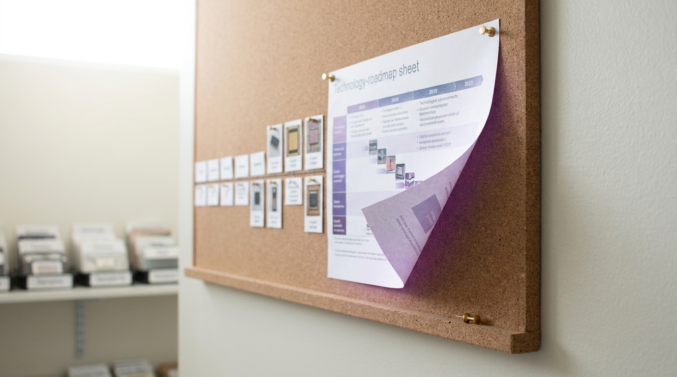
Figure 2. The roadmap is a real sheet of paper in a real room, revised by hand, and its most recently touched corner is the one still curling. — Image prompt and art direction by Brecht Corbeel; generation pending.
Analysis. The more granular figures behind that roadmap show what CFET is actually buying, and expose the assumption underneath the 2033 date. Reporting on the same 2026 forum gives contacted poly pitch (CPP) and standard-cell height across successive nodes: A14 in 2028 at roughly 45-nanometre CPP and 115-nanometre cell height, with High-NA EUV introduced at that stage; A10 around 2030 holding CPP near 42 nanometres, a point past which “further scaling of CPP is expected to face fundamental limitations”; A7 — CFET’s likely starting point, with adoption itself described as uncertain — at that same 42-nanometre CPP; and A5, arriving around 2035–2036, still at 42-nanometre CPP but with cell height down to roughly 64 nanometres [6]. Layout density is, to a first approximation, inversely proportional to the area of one contacted cell, which scales with pitch times cell height:
D \propto \frac{1}{\mathrm{CPP} \times H_{\mathrm{cell}}}
Treat this as a simplified proportionality, not a physical law — real layout density also depends on track count, via pitch and design-rule detail this expression ignores. Applied to imec’s own published figures, it makes the assumption behind the CFET scenario explicit. Between A14 (2028) and A5 (2035–2036), CPP shrinks by only about 7 percent (45 to 42 nanometres) while cell height shrinks by roughly 44 percent (115 to 64 nanometres), together implying close to a 93 percent density gain over that span [6] — almost all of it arithmetically attributable to cell-height and architecture change, not to lithographic pitch. CFET’s economic case rests on exactly that arithmetic: it buys cell-height reduction, which is why the roadmap can hold CPP essentially flat across A10, A7 and A5 while still projecting a rising density curve. Note also what the roadmap does not resolve: A5, the first full node after CFET’s stated A7 introduction, sits inside this article’s 2035 horizon, and CFET adoption at A7 is explicitly flagged as uncertain. No leading logic manufacturer besides imec’s own roadmap appears to have published its own calendar year for CFET production; 2033 is imec’s institutional projection for its member ecosystem, not a manufacturer’s shipping commitment.
Scenario A — CFET arrives close to plan. At least one leading manufacturer ships a CFET-based node within roughly two years of imec’s 2033 figure. Assumptions: sequential or monolithic CFET integration reaches manufacturable defect rates on the timeline imec’s DTCO studies imply, and no cheaper alternative removes the economic pressure to move at A7. Indicators: IEDM and foundry disclosures naming a specific CFET production node and ship date. Disconfirmed if no manufacturer has disclosed a CFET production commitment by 2033.
Scenario B — CFET slips past the horizon. CFET remains a prototype and DTCO-study technology through 2035, with density gains instead coming from nanosheet and forksheet refinements plus backside power delivery, and “A7” comes to describe a marketing generation whose transistor is still, structurally, a lateral device. Assumptions: monolithic CFET’s bonding, isolation and contact challenges prove harder to resolve at manufacturable yield than imec’s roadmap currently implies. Indicators: repeated roadmap revisions pushing CFET’s stated introduction later at successive imec forums. Disconfirmed if a CFET production node ships before 2033 at any manufacturer.
Prediction. Horizon: 31 December 2035. At least one leading-edge logic manufacturer will have shipped a CFET-based node in commercial volume, but CFET will not yet be the default architecture industry-wide — nanosheet or forksheet devices will still account for the majority of leading-edge logic volume shipped in 2035. Assumption: density gains available from cell-height and track-count reduction alone remain sufficient to justify delaying full CFET conversion at nodes where it is not yet required. Indicator: published node-architecture disclosures across leading logic manufacturers’ 2033–2035 shipping products. Disconfirmed if, by the horizon, either no manufacturer has shipped a CFET product, or CFET has already become the majority leading-edge architecture.
Where the wafers get made: diversification without dilution
Fact. Three separate, verifiable capital programmes are adding leading-edge or near-leading-edge logic capacity outside the two economies — Taiwan and South Korea — that have concentrated it for two decades. In Arizona, under a U.S. Department of Commerce CHIPS Act award of up to 6.6 billion dollars in direct funding plus up to 5 billion dollars in loans, TSMC is building three greenfield fabs at a combined investment over 65 billion dollars: the first began production on 4-nanometre and 5-nanometre FinFET processes in the first half of 2025, the second is due to begin 3-nanometre FinFET production in the second half of 2027, and the third is planned for A16 and 2-nanometre nanosheet processes by the end of the decade [12]. In Hokkaido, Rapidus began prototype production of 2-nanometre-class gate-all-around transistors at its IIM-1 facility on 19 July 2025, having gone from a September 2023 groundbreaking through a completed cleanroom in 2024, an installed EUV tool that December, and a first EUV exposure in April 2025, with more than 200 machines running by mid-2025; the company’s stated plan is to bring advanced customers on within roughly three quarters and reach volume manufacturing in 2027 [13]. Both are real fabs running real wafers, not announcements.
Fact — the broader spending picture. SEMI’s mid-2026 forecast projects worldwide 300-millimetre fab equipment spending rising 18 percent to 133 billion dollars in 2026 and a further 14 percent to 151 billion dollars in 2027 — the first year that figure has crossed 150 billion — describing the investment as “broadly distributed across the major semiconductor manufacturing regions” through 2029: continued domestic expansion in China, continued leading-edge foundry expansion in Taiwan, memory-tied investment in Korea, advanced-process expansion in the Americas, and “meaningful growth” forecast for Japan, Europe, the Middle East and Southeast Asia [11]. Over 2027–2029 the same forecast puts Logic and Micro spending at roughly 228 billion dollars and Memory at roughly 175 billion, split 111 billion in DRAM and 62 billion in 3D NAND [11].
Figure 3. The industry's geography shows up here first — as a pod from a different site, still half inside its crate. — Image prompt and art direction by Brecht Corbeel; generation pending.
Analysis. Diversification and concentration describe two different axes, and the facts above sit on different sides of each. Location is genuinely diversifying: Arizona and Hokkaido did not host leading-edge logic fabrication five years ago, and now each does or soon will. Ownership is not diversifying at anything like the same rate — the Arizona fab is TSMC’s, running TSMC’s process under TSMC’s control, and the Hokkaido fab exists specifically because Rapidus licensed IBM’s 2-nanometre gate-all-around process rather than developing an independent one. SEMI’s own regional breakdown gives growth rates and rough spending totals but not the installed base of leading-edge capacity by region or company [11], so the headline “broadly distributed” spending figure does not, by itself, demonstrate that leading-edge capability has spread beyond the organisations that have always held it. A new country hosting a fab and a new company entering the leading edge are different kinds of diversification; the evidence here supports the first far more strongly than the second. Rapidus’s own 2027 target also trails the point at which TSMC and Samsung were already ramping 2-nanometre-class production by roughly two years — a real, if modest, gap between the newest entrant and the incumbents it is trying to join.
Scenario A — geography spreads, control stays narrow. By 2035, meaningful leading-edge logic volume runs in the United States and Japan alongside Taiwan and Korea, but every one of those fabs is operated by one of the same organisations — TSMC, Samsung, Intel, Rapidus — capable of leading-edge logic in 2026: location diversifies, the competitive set does not. Assumptions: export-control regimes continue to prevent a genuinely new entrant, particularly a Chinese national champion, from reaching leading-edge capability within the horizon. Indicators: wafer-start volumes and node capability disclosed at non-Taiwan, non-Korea fabs, cross-checked against the roster of organisations capable of the same node elsewhere. Disconfirmed if a fifth, previously non-leading-edge organisation independently reaches leading-edge logic capability before 2035.
Scenario B — subsidised capacity stays structurally behind. Politically motivated capacity in the U.S. and Japan continues to trail the process frontier by a persistent one-to-two-generation gap, because the deepest process know-how remains concentrated at each company’s home campus regardless of where its newest buildings sit. Assumptions: the tacit, hard-to-transfer engineering knowledge behind yield ramp continues to travel slower than capital and equipment do. Indicators: the calendar gap between a node’s introduction at its home campus and its introduction at a non-home-country fab. Disconfirmed if a non-home-country fab introduces a leading-edge node within the same calendar year as its originating company’s home fab.
Prediction. Horizon: 31 December 2035. At least one fab located outside Taiwan and South Korea will be running leading-edge (2-nanometre-class or beyond) logic production at commercial volume, not merely risk or pilot production, but the set of organisations capable of leading-edge logic worldwide will still number four or fewer. Assumption: no additional organisation, inside or outside today’s export-control regimes, closes the leading-edge capability gap within the horizon. Indicator: published wafer-start volumes and process-node disclosures from Arizona, Hokkaido and any comparable non-incumbent-region site, cross-checked against the roster of organisations capable of the same node elsewhere. Disconfirmed if, by the horizon, either no non-Taiwan/Korea fab has reached leading-edge volume production, or a fifth independent organisation has reached leading-edge capability.
The channel material after silicon
Fact. imec’s published logic-scaling roadmap treats two-dimensional transition-metal-dichalcogenide (TMD) channel materials — principally molybdenum disulfide (MoS₂) for n-type devices and tungsten diselenide or tungsten disulfide (WSe₂, WS₂) for p-type devices — not as a near-term replacement for silicon across the whole transistor, but as a staged introduction: first at the A7 node in less demanding peripheral back-end-of-line roles such as voltage regulators and power switches, with broader integration folded into a heterogeneous “CMOS 2.0” architecture only expected around A3, and integration into full CFET structures pushed later still [7]. The same article names three unresolved “most critical obstacles”: fab-compatible source/drain contact formation, controllable doping, and enabling functioning CMOS logic with these materials at all [7].
Fact — the recent signal. Two results within six months of each other mark real, verifiable progress against exactly those obstacles. At IEDM in December 2025, imec reported a WSe₂ p-type transistor reaching a maximum drive current of 690 microamps per micron, developed with TSMC on gate-stack integration and with Intel on a fab-compatible, damascene-style top-contact process imec calls a world first, aimed specifically at 300-millimetre manufacturability [8]. In June 2026, a joint imec, ASML and TSMC effort went further, demonstrating complementary — both n-type and p-type — 2D-material transistors at a 50-nanometre contacted poly pitch across a full 300-millimetre wafer, with 94 percent of devices electrically functional at an on/off current ratio above 100,000, in a process imec describes as “scalable, back-end-compatible 300mm integration” [9].
Institutional claim. imec frames that June 2026 result as “a crucial step in the lab-to-fab transition of 2D-material based transistors” [9] — its own characterisation of the milestone, made by the organisation that ran the demonstration together with two of its commercial partners.
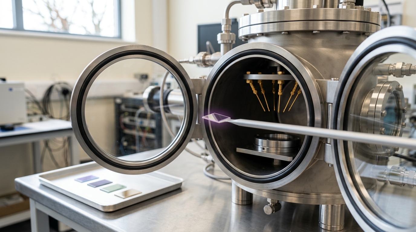
Figure 4. Every channel-material claim in this section reduces to a coupon like this one, still outside the chamber it needs to prove itself inside. — Image prompt and art direction by Brecht Corbeel; generation pending.
Analysis. A peer-reviewed review published the same year in Nano Letters reads the same technology class more cautiously. Zheng, Meng and Li confirm the physical case for TMDs — their smooth, saturated surface bonding gives “the possibility of achieving superior channel-to-dielectric interfaces” compared to silicon, and MoS₂, WSe₂ and WS₂ each show markedly higher electron mobility than silicon at comparable thickness [10] — but conclude plainly that “2D materials are still in the early stages of development for transistor applications,” naming unresolved contact resistance (especially for p-type devices), immature large-area synthesis at industrial 8- to 12-inch wafer scale, transfer processes that damage the material, and defect-density control as open problems, and stating that “a proper growth tool for delivering uniform, low-defect-density, wafer-scale, and single-crystalline 2D materials is urgently needed and yet to be developed” [10]. Both accounts can be true at once: a single 50-nanometre-pitch demonstration wafer is a genuine engineering milestone, and the industrial growth-and-transfer infrastructure needed to run that process at fab volume and yield is, on the independent literature’s own account, still missing.
Scenario A — the phased roadmap holds. 2D materials enter production exactly where imec’s roadmap places them: narrow, peripheral back-end-of-line roles near A7 (around 2033), with broader logic integration still pending at the 2035 horizon. Assumptions: the wafer-scale growth-tool gap the peer-reviewed literature identifies closes on roughly the timeline imec’s roadmap implies. Indicators: foundry disclosures naming 2D-material devices in shipped peripheral or BEOL roles. Disconfirmed if no 2D-material device reaches any commercial product role by 2033.
Scenario B — the materials-supply gap holds it back further. The named gap — a mature, uniform, low-defect wafer-scale growth tool — remains unresolved past 2035, because it is a materials-science and equipment problem distinct from the device-integration progress imec’s demonstrations represent, and even the narrow peripheral insertion point slips past the horizon. Assumptions: device-level demonstrations continue outpacing materials-supply infrastructure, the harder and less headline-friendly problem. Indicators: the continued absence of a named, qualified 300-millimetre 2D-material growth tool from any major equipment vendor. Disconfirmed if a qualified production growth tool for wafer-scale 2D materials is commercially available before 2033.
Prediction. Horizon: 31 December 2035. No logic manufacturer will have shipped a commercial product using a 2D material as the primary channel for its main compute transistors; if 2D materials appear in any shipped product by then, it will be in a peripheral or back-end-of-line role, consistent with imec’s own staged plan. Assumption: no unpublished breakthrough in wafer-scale, low-defect TMD growth — the specific gap the peer-reviewed literature names — is achieved and industrialised faster than the roadmap implies. Indicator: IEDM and foundry disclosures naming the channel material used in each newly announced production logic node. Disconfirmed if a foundry ships a production node before 2035 using a 2D material as the primary channel for its main compute path.
What would actually force a discontinuity
Fact. Canon’s nanoimprint lithography (NIL) tool, the FPA-1200NZ2C, works by mechanically pressing a patterned quartz template into resist rather than projecting an image through optics. Canon has shipped its first commercial unit — delivered in late 2024 to the Texas Institute for Electronics, a facility backed by Intel, NXP, Samsung and DARPA — with a demonstrated minimum linewidth of 14 nanometres, roughly a 5-nanometre-node equivalent, and a stated roadmap toward 10 nanometres, roughly a 2-nanometre-node equivalent [14]. Canon’s own account frames the appeal as both cost and energy — a stamped pattern needs none of EUV’s reflective optics, vacuum chamber or plasma light source — and the company has said it targets producing ten to twenty NIL systems a year within three to five years, with memory maker Kioxia named as an early prospective customer [14].
Vendor claim. That cost-and-simplicity case is Canon’s own, and it is worth taking at face value as a claim about the mechanism’s physical simplicity — projecting a pattern through six reflective mirrors under vacuum genuinely does carry more inherent complexity than pressing a template into resist.
Analysis. Independent technical assessment finds that simplicity has not yet translated into a competitive advanced-logic tool. Trade reporting on NIL’s current state finds template lifetimes running “in the order of fifty wafers in real-world use,” well short of manufacturer claims, because the pressing process causes “mechanical stress, breakage and particle generation” on the template’s finest features; that NIL’s overlay error is roughly four times larger than advanced logic requires, a gap needing “an overhaul of the architecture of Canon’s NIL tool” rather than incremental tuning; that sufficiently sharp, smooth mask features at the nanometre scale remain unresolved, with residual roughness translating directly into line-edge roughness and consequent wire shorts, leakage or performance loss; and that throughput — roughly 25 wafers per hour, or about 100 in a clustered configuration — trails EUV scanners already running at least twice as fast, with ASML targeting higher speeds still [15]. The same reporting concludes these combined gaps make NIL “unsuitable and not cost-effective for production at the advanced nodes” today [15]. Kioxia’s interest, and Canon’s own emphasis on memory, are consistent with that assessment: memory structures are more repetitive and more overlay-tolerant than logic, exactly where a mechanically simpler but currently less precise technique is most likely to find its first real production use.
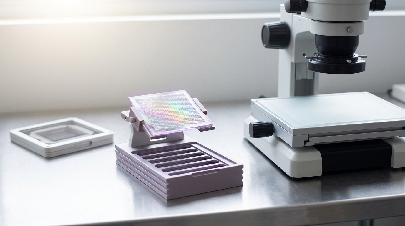
Figure 5. A genuine discontinuity would have to clear an inspection bench like this one, not just a press release; today the template is out of its cassette and the microscope is still empty. — Image prompt and art direction by Brecht Corbeel; generation pending.
Scenario A — NIL stays a memory-and-niche technology. By 2035, nanoimprint lithography is in real production use for NAND flash or other memory structures with relaxed overlay requirements, but has not displaced EUV for any leading logic layer, because the overlay, template-lifetime and throughput gaps documented above are mechanism-level limits rather than engineering polish. Assumptions: no fourth-generation NIL architecture closes the fourfold overlay gap within the horizon. Indicators: announced NIL production deployments broken out by device type. Disconfirmed if a leading-edge logic manufacturer qualifies NIL for any production logic layer before 2035.
Scenario B — a genuine discontinuity emerges from elsewhere. Neither High-NA EUV’s incremental aperture gains nor NIL’s current limitations turn out to matter, because a technology outside the first two trajectories — directed self-assembly used as a genuine pitch-multiplying complement to EUV, or an approach not yet publicly disclosed — reaches production readiness inside the horizon and changes which constraints bind. This scenario is deliberately the hardest of the five to attach a specific indicator to, because a genuine discontinuity is disclosed later than an extrapolated trend is. Indicators: any patterning technology reaching disclosed production qualification that is not EUV, High-NA EUV, or an extension of established multiple patterning. Disconfirmed if no such technology reaches production qualification by 2035, in which case the industry’s patterning toolkit in 2035 will be recognisably the same toolkit it has today, extended rather than replaced.
Prediction. Horizon: 31 December 2035. Nanoimprint lithography will have reached real production volume in memory or a comparably overlay-tolerant application, but will not have been qualified for any leading-edge logic layer at a top-tier foundry. Assumption: the named gaps in template lifetime, overlay and throughput are mechanism-level limits of the pressing approach rather than solvable engineering detail. Indicator: disclosed production qualifications of NIL broken out by device type. Disconfirmed if, by the horizon, either NIL has failed to reach any production use at all, or it has been qualified for a leading-edge logic layer.
What to take away
Five trajectories, five different clocks. High-NA EUV has already shipped in volume at one company while its two largest rivals have made visibly different bets about when — or whether soon — to follow [1, 3]. CFET has a specific institutional date, 2033, attached to it by the one organisation whose roadmap the industry treats as a shared reference point, and that roadmap’s own numbers show the date resting on cell-height and architecture gains rather than on lithographic pitch [5, 6]. New fab capacity is genuinely arriving outside Taiwan and Korea, in real buildings running real wafers, without yet diversifying who is capable of leading-edge logic at all [12, 13]. Two-dimensional channel materials have cleared a real, specific pitch-and-yield milestone on a 300-millimetre wafer while the independent literature still calls the underlying materials-supply base immature [9, 10]. And the most publicly visible candidate for a genuine patterning discontinuity has a named, mechanism-level gap between its vendor’s claims and what independent assessment finds it can currently do [14, 15].
None of that adds up to a single 2035. It adds up to five falsifiable claims, each checkable well before the horizon arrives, each stated here in a form specific enough to be wrong. That specificity is the point: a scenario that cannot fail is not a scenario, and a fabrication roadmap that only ever turns out to have been directionally right was never really tested at all.
Sources
- ASML. High NA EUV reaches new readiness milestone. ASML (2026).
- Hank Hogan. Turning another EUVL resolution knob. SPIE (2025).
- TrendForce. ASML Confirms First High-NA EUV EXE:5200 Shipment, Reportedly Prepping for Intel's 14A in 2027. TrendForce (2025).
- imec. CFET (complementary FET). imec (2022).
- Samuel K. Moore. Imec Semiconductor Technology Roadmap: CFETs in 2033. IEEE Spectrum (2026).
- TrendForce. imec Roadmap Extends to A3 by 2038; Chip Density Gains Shift Beyond Traditional Transistor Scaling. TrendForce (2026).
- imec. 2D-material based devices in the logic scaling roadmap. imec (2025).
- imec. Imec Advances 2D-material Based Device Technology Beyond State of the Art in Support of the Future Logic Technology Roadmap. imec (2025).
- imec. 2D-material transistors closer to industrial readiness. imec (2026).
- Fangyuan Zheng, Wanqing Meng, and Lain-Jong Li. Continue the Scaling of Electronic Devices with Transition Metal Dichalcogenide Semiconductors. Nano Letters (2025). DOI: 10.1021/acs.nanolett.4c06007.
- SEMI. SEMI Projects Double-Digit Growth in Global 300mm Fab Equipment Spending for 2026 and 2027. SEMI (2026).
- National Institute of Standards and Technology. TSMC Arizona. NIST CHIPS Program Office (2024).
- ServeTheHome. Rapidus Starts 2nm Gate All Around Prototype Production at IIM-1. ServeTheHome (2025).
- Techzine. China chases Canon's chipmaking process as ASML alternative. Techzine Global (2025).
- Paul van Gerven. Nanoimprint lithography won't compete with EUV anytime soon. Bits&Chips (2025).
Originally published at https://absolutedigitalpublishers.com/articles/advanced-semiconductor-fabrication-in-2035-scenarios-signals-and-falsifiable-predictions.