A "2-Nanometer" Chip Has No 2-Nanometer Feature, and the Gap Is Widening
TSMC's N2, Samsung's SF2, and Intel's 18A all shipped in the same eighteen months, all get called "2-nanometer," and none of them has a single physical feature anywhere near two nanometers.

Every "nanometer" in a node's marketing name traces back to a page like this one somewhere — and the number actually circled on it is never the number printed on the box. — Image prompt and art direction by Brecht Corbeel; image generated to that direction.
Abstract
Gate pitch on TSMC's N2 is 48 nanometers. On Samsung's SF2 it's 50. On Intel's 18A it's 50. All three ship inside the same eighteen-month window under a marketing name that means "two nanometers." This article does not repeat the now-familiar observation that node names are marketing — it builds and tests a number that would still mean something even after that observation is granted. Using Intel's own disclosed transistor-density figures across nine node generations (2005-2024) and TSMC's across six (2016-2025), it constructs a Node Reality Ratio — measured density divided against the 2x-every-24-months curve the industry itself uses as its definition of "on schedule" — and finds both foundries' own numbers falling from roughly 70-90 percent of that pace in the mid-2010s to under 22 percent by their most recent disclosed nodes. A single node, Intel's 10-nanometer generation, turns out to carry two official density figures nearly twice apart depending on whose counting formula is used. And the IEEE's own 2024 roadmap — not a retrospective complaint, a forward plan — projects zero change in gate pitch across four consecutive future node labels.
TSMC calls its newest logic process N2. Samsung calls the process it ships in the same eighteen-month window SF2. Intel calls its own entrant 18A, which Intel’s own marketing reads as “1.8-angstrom-class” — a small enough number that “nanometer” has quietly given way to “angstrom” as the unit doing the bragging. All three are described in industry shorthand as “2-nanometer” chips. None of them has a gate pitch anywhere near two nanometers. TSMC’s N2 carries a contacted gate pitch reported at 48 nanometers; Samsung’s SF2 and Intel’s 18A are both reported around 50 [1]. Whatever else those three numbers disagree about, they agree on this: the smallest repeating physical feature on a “2-nanometer” chip is roughly twenty-five times larger than two nanometers, on all three of the companies competing to sell it to you.
This is not a new observation, and this article does not pretend it is one. Wikipedia’s own technical articles on these process nodes state the point flatly and have for years: “process nodes have been named purely on a marketing basis” since the late 1990s, with “no relation to the dimensions on the integrated circuit” [7, 5]. Everyone who follows this industry past its press releases already knows the number after “nm” is a name, not a measurement. What nobody has done with that concession is ask the next question honestly: if the label is gone, is there still a real number underneath it that behaves the way Moore’s Law always claimed a chip-scaling number should — doubling on a predictable clock? And if there is, has it kept that clock, or has it been quietly falling behind the same way the label stopped meaning anything?
There is such a number. It is areal transistor density — how many transistors a foundry can actually pack into one square millimeter of finished silicon — and unlike “nanometer,” foundries still disclose it, generation after generation, in their own investor and technical materials. Built from Intel’s own disclosed density figures across nine node generations spanning 2005 to 2024, and TSMC’s own disclosed figures across six generations spanning 2016 to 2025, this article constructs what I’ll call the Node Reality Ratio: measured density divided by the density Moore’s Law would predict if the industry’s own long-stated doubling-every-two-years pace had simply continued unbroken from a fixed, disclosed starting point. The ratio should sit near 1.0 if the industry is still on the clock it has always claimed to be on. It does not. By each foundry’s own numbers, it has fallen under 0.22 — meaning real, foundry-disclosed density is now running at under a quarter of the pace the industry’s own historical doubling rate would predict.
The Number Was Never Meant to Be a Ruler Measurement
Contacted gate pitch, minimum metal pitch, and standard-cell height are three separate physical dimensions, cut in three separate steps of the manufacturing process, and none of them alone is what “2 nanometers” was ever supposed to describe even in the industry’s own internal terminology. The IEEE’s International Roadmap for Devices and Systems, the standards body that succeeded the old International Technology Roadmap for Semiconductors, states this directly in its own 2024 update: gate pitch, metal pitch, fin pitch, and gate length are each tracked as independent “key parameters,” and “there is not yet a consensus on the node naming across different foundries and integrated device manufacturers” — the roadmap’s own words, describing its own industry, in a document published for engineers rather than customers [11]. Areal transistor density, the quantity a chip designer actually cares about, is the product of those pitches multiplied together with standard-cell height and whatever fraction of the layout logic actually occupies rather than routing or spacing — which is exactly why a single figure like “gate pitch” was never going to summarize it, and exactly why a single word like “nanometer” was never going to summarize gate pitch, metal pitch, and cell height simultaneously. Three numbers were compressed into one syllable, and the compression is where the marketing lives.
That collapse used to matter less than it does now, because for roughly three decades — from the first commercial microprocessors through the mid-2000s — gate pitch, metal pitch, and transistor density all shrank together, closely enough in step that treating “the node number” as a rough proxy for “how much smaller is this chip’s stuff” was a survivable simplification. The historical record here is Intel’s own, because Intel is the one company that has disclosed a comparable density figure, using a comparable internal methodology, across essentially every node it has shipped since the mid-2000s. That continuity is what makes it possible to build a real time series rather than stitching together numbers that were never meant to compare.
Intel’s Own Twenty Years, Run Through the Doubling Clock
Intel’s 65-nanometer process, which began shipping in 2005, is disclosed at a transistor density of 2.08 million transistors per square millimeter (MTr/mm²) [10]. Intel’s 45-nanometer process, which reached mass production in November 2007 on the Xeon 5400 series, is disclosed at 3.33 MTr/mm² [9]. Its 32-nanometer process, ramping through 2009 into 2010, is disclosed at 7.11 MTr/mm² [8]. Its 22-nanometer Tri-Gate process — Intel’s first commercial FinFET, first shipped in Ivy Bridge processors in April 2012 — is disclosed at 16.5 MTr/mm² [7]. Its 14-nanometer process, reaching mass production in the fourth quarter of 2013, is disclosed at 33.8 MTr/mm² [6]. Its Intel 4 process, shipping in 2023, is disclosed in a range of 123.4 to 129.8 MTr/mm² [3]. Its Intel 3 process, reaching mass production in the second quarter of 2024, is disclosed at 143.37 MTr/mm² [2]. Seven generations, nineteen years, one company’s own disclosed numbers.
Set a baseline at the earliest of those points — 2.08 MTr/mm² in 2005 — and ask what density Intel’s own historical doubling claim would predict for each later year, using the industry-standard framing of a doubling every 24 months: predicted density equals 2.08 times two raised to the power of (years elapsed divided by two). That arithmetic gives a specific, checkable number for every year in the table, and the ratio of what Intel actually shipped to what that formula predicts is the Node Reality Ratio for that generation.
- Node — Year — Actual density (MTr/mm²) — 2×/24-month prediction — Node Reality Ratio
- 65nm — 2005 — 2.08 — 2.08 — 1.00
- 45nm — 2007 — 3.33 — 4.16 — 0.80
- 32nm — 2010 — 7.11 — 11.77 — 0.60
- 22nm (Tri-Gate) — 2012 — 16.5 — 23.53 — 0.70
- 14nm — 2014 — 33.8 — 47.06 — 0.72
- 10nm (standard count) — 2018 — 52.51 — 188.30 — 0.28
- Intel 4 — 2023 — 126.6 (midpoint) — 1,065.0 — 0.12
- Intel 3 — 2024 — 143.37 — 1,506.1 — 0.095
Two things about that table are worth stating plainly before drawing a conclusion from it, because both cut against overreading it. First, the ratio does not fall in a straight line — it recovers slightly at 22nm and 14nm, the two nodes bracketing Intel’s own FinFET introduction, before its real collapse. That texture is the data, not noise to be smoothed away: whatever caused the later collapse was not simply “FinFET stopped working,” since FinFET’s first two generations briefly outperformed the trend the two prior planar nodes had set. Second, the last three rows compound an exponential prediction over thirteen to nineteen years, which means the predicted values in the 2018-2024 range are dominated almost entirely by how fast the very early denominator was set — a modeling choice I return to directly in the counter-case below, because it is the strongest available objection to this whole construction, not a footnote to bury.

Figure 1. Gate pitch, metal pitch, and cell height are three separate dimensions, cut by three separate processes, on three separate schedules. A single "node number" was always trying to average them into one syllable. — Image prompt and art direction by Brecht Corbeel; image generated to that direction.
With that stated, the shape holds regardless of exactly where the exponential curve is anchored: Intel’s own density numbers ran at 60 to 80 percent of a flat doubling pace through 2014, then fell to roughly a quarter of that pace by 2018, and to under a tenth of it by 2024. That is not a story about node names losing meaning. Node names losing meaning was already conceded in the second paragraph of this article. This is a story about the one quantity that survives the naming collapse — the thing marketing was trying, badly, to gesture at — running measurably behind the rate its own maker used to hit.
A Second Company, a Different Clock, the Same Direction
One company’s numbers could be an artifact of one company’s specific stumble — Intel’s well-documented multi-year delay bringing its 10-nanometer process to volume production is, after all, a large part of why that row shows such a steep drop. The dossier for this piece flags exactly that risk, and the honest response is to check a competitor that did not share Intel’s delay.
TSMC’s 10FF process, its first 10-nanometer-class node, reached its initial production ramp in the fourth quarter of 2016 at a disclosed density of 51.82 MTr/mm² [5]. Its N7 process, reaching mass production in 2018, is disclosed in a range of 91.2 to 96.5 MTr/mm² [4]; the midpoint, 93.85, is used below. Its N5 process, shipping from 2020, is disclosed at 138.2 MTr/mm² [3]. Its N4 process, shipping from 2022, is disclosed at 143.7 MTr/mm² [3], while its N3 process, reaching mass production the same year, is disclosed at 197 MTr/mm², and its refined N3E process, shipping from late 2023, at 216 MTr/mm² [2]. Running the identical doubling-clock arithmetic against TSMC’s own 2016 baseline:
- Node — Year — Actual density (MTr/mm²) — 2×/24-month prediction — Node Reality Ratio
- 10FF — 2016 — 51.82 — 51.82 — 1.00
- N7 — 2018 — 93.85 (midpoint) — 103.64 — 0.91
- N5 — 2020 — 138.2 — 207.28 — 0.67
- N4 — 2022 — 143.7 — 414.56 — 0.35
- N3 — 2022 — 197 — 414.56 — 0.48
- N3E — 2023 — 216 — 586.30 — 0.37
TSMC’s own numbers never touched Intel’s 10-nanometer stumble, ran on a different internal roadmap, used a different fin and cell architecture across most of this span, and still trace the identical shape: a ratio close to 1.0 at the earliest point in the series by construction, falling into the 0.6-0.9 range through the late 2010s, then dropping into the 0.35-0.5 range as the node names moved into single digits. Two companies, two unrelated engineering histories, two independently disclosed density series, one converging answer.
TSMC’s own newest disclosure extends the pattern one generation further, though with a caveat worth stating in the open rather than smoothing over. TSMC has disclosed that N2 delivers an “aggregate” transistor-density increase of 15 percent over N3, alongside up to 15 percent better performance or up to 35 percent better energy efficiency at matched conditions, and an SRAM density of 38 megabits per square millimeter — an 11 percent improvement over N3 [12]. TSMC has not, in any source this article could independently verify, disclosed a single absolute MTr/mm² figure for N2 the way it did for N3 and N3E. Applying its own disclosed 15 percent uplift to N3’s disclosed 197 MTr/mm² gives a derived estimate of roughly 226.6 MTr/mm²; applying it to N3E’s 216 gives roughly 248.4. A third figure circulates in general industry commentary — close to 313 MTr/mm² — that this article could not reconcile against TSMC’s own stated 15 percent figure using either N3 or N3E as the base, and it is deliberately not used here. Using the more conservative 248.4 estimate, derived directly from TSMC’s own disclosed percentage rather than borrowed from an unreconciled third-party number, against a 2025 mass-production date: predicted density is 1,172.7 MTr/mm², giving a Node Reality Ratio of 0.21 — continuing the fall, not reversing it, and doing so on a number this article computed itself rather than one TSMC disclosed outright, a distinction worth keeping visible rather than blurring.

Figure 2. Both circles claim to describe the density of the same node. One formula gives roughly 53 million transistors per square millimetre. The other, applied by the same company to the same chip, gives roughly 101 million. Neither circle is the fraud; the single word "density" is the one doing too much work. — Image prompt and art direction by Brecht Corbeel; image generated to that direction.
The Same Node, Counted Two Ways, Gives Two Different Answers
Row six of the Intel table above hides something the raw arithmetic does not show, and it is the sharpest single illustration in this article of how far “density” itself has drifted from being one clean number. Intel’s 10-nanometer process has two officially disclosed density figures. Counted by the industry-standard method most other foundries’ figures in this article use, it comes to 52.51 MTr/mm². Counted by Intel’s own separately disclosed formula — a different weighting of standard logic-cell types, not a different chip — it comes to 100.76 MTr/mm² [5]. Neither number is fabricated. Both were disclosed by Intel, about the same process, describing the same shipping silicon. They differ by very nearly a factor of two, and the difference exists entirely because “density” is not actually one measurement — it is a weighted average over an assumed mix of standard-cell types, and the weights are a choice, not a physical constant.
Recomputed with Intel’s own preferred 100.76 figure instead of the industry-standard 52.51, the 2018 Node Reality Ratio rises from 0.28 to 0.53 — still well under the 0.60-0.80 range Intel’s own earlier nodes held, but no longer the article’s most dramatic single number. That range itself, 0.28 to 0.53 for the same node measured two honest ways, is the point. If two disclosures from the same company, about the same process, produce a near-two-fold spread in the one number this whole article is built on, then whatever residual precision the phrase “transistor density” seems to promise over the phrase “10 nanometers” is smaller than it looks — real, and still far more meaningful than a marketing label, but not the clean physical ruler measurement gate pitch and metal pitch alone might suggest either. This is not a reason to abandon density as the better metric. Gate pitch and metal pitch are unambiguous physical distances that a scanning electron microscope can measure directly off a cross-section, which is exactly why this article leans on the disclosed pitch and density figures that trace back to physical measurement rather than on the marketing label built to obscure it — density is simply the more complicated of the two, and its complications deserve to be named rather than hidden inside a single unqualified figure.
The Roadmap Itself Already Plans for This to Continue
Everything above is a retrospective reading of numbers the industry has already shipped. The strongest version of this article’s claim is not retrospective at all — it is sitting inside the standards body’s own forward-looking plan, published this year, for nodes that have not shipped yet.
IRDS’s 2024 More Moore roadmap lays out nine planned technology generations from 2024 through 2039, each labeled with both a technical code — using the notation “Gxx: contacted gate pitch, Mxx: tightest metal pitch in nm” — and a separate “logic industry node range” label meant to approximate how the generation will likely be marketed [11]. The document’s own disclosed Gate Pitch row, reproduced exactly from Table MM-7, reads: 48, 48, 48, 48, 46, 44, 44, 42, 42 nanometers, for the years 2024, 2025, 2027, 2029, 2031, 2033, 2035, 2037, and 2039 respectively. Lined up against the marketing labels the same table assigns those same years — “3nm” Enhanced, “2nm,” “1.4nm,” and “A10 eq” — the gate pitch is identical, 48 nanometers, across all four of those generations [11]. The roadmap plans for the marketing name to move through four full generations while the specific dimension gate pitch is meant to describe does not move at all.
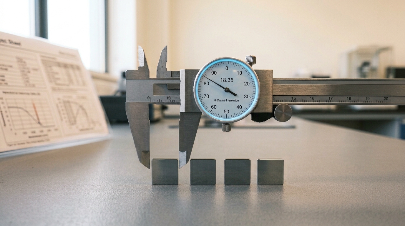
Figure 3. Four future node generations, by the standards body's own 2024 roadmap, share this exact gate-pitch spacing. Only the marketing name printed beside each tab is scheduled to change. — Image prompt and art direction by Brecht Corbeel; image generated to that direction.
This is not this article’s inference about a document’s implications. It is the document’s own table, read directly off the page: four rows in a nine-column table, same number, four different node names above them. The roadmap’s own explanatory note anticipates the objection that gate pitch alone cannot be the whole story — “on top of pitch scaling there are other elements such as cell height, number of stacked devices, DTCO constructs, 3D integration, etc. that define the target area scaling” [11] — and the table’s own numbers show exactly that kind of substitution already planned: the finest interconnect pitch in the same table (the row IRDS labels “Mx pitch”) does continue shrinking across those same years, from 32 nanometers in 2024 down to 20 by 2029, even while gate pitch sits still. The industry is not claiming gate pitch will keep shrinking at the old pace and calling that “2nm.” It is planning to hold gate pitch flat, shrink a different dimension instead, and let the marketing label imply that the first dimension moved anyway. That is not a retrospective failure this article discovered after the fact. It is a documented forward plan, in the standards body’s own words, for the exact pattern this article’s historical data already shows.
The Strongest Objection, Stated Rather Than Buried
The most serious challenge to everything above is not that any individual number is wrong. It is that “transistor density” may never have been one clean, comparable metric even in the eras this article treats as the well-behaved baseline. SRAM bit-cell density, logic-only density, and blended “aggregate” density genuinely differ — sometimes by 20 to 30 percent within the same node, the way TSMC’s own N2 disclosure distinguishes an aggregate mixed-design figure from a logic-only figure expected to run higher — and the specific point at which independent, cross-comparable teardown data became available from firms like TechInsights may simply be later than this article’s 2005-2010 baseline nodes, meaning the apparent mid-2010s inflection could partly reflect when good comparable data started existing rather than when real industry behavior changed. A critic could reasonably argue this article’s exponential baseline, anchored on a single 2005 data point and compounded for nineteen years, is doing more work than any single number should be trusted to do — small uncertainty in that one anchor compounds into large uncertainty in the predicted values for 2023 and 2024, exactly the years carrying this article’s most dramatic ratios.
That objection is worth taking seriously rather than rebutting reflexively, and it is why this article leans as hard as it does on the shape shared by two independent foundries’ two independently disclosed density series, rather than resting everything on Intel’s numbers alone, and why it treats the IRDS roadmap’s flat-gate-pitch finding as the strongest single piece of evidence — because that finding does not depend on any exponential baseline, any compounding, or any comparability assumption across decades of teardown methodology. It is one document, one table, four rows, read once. The historical Node Reality Ratio construction and the forward IRDS-table finding are two separate arguments that do not share the same vulnerability, and a reader unconvinced by the compounding-arithmetic critique of the first should weigh the second on its own, much shorter, harder-to-dispute terms.
What Would Prove This Wrong
This article’s central claim is a specific, near-term, falsifiable one: the Node Reality Ratio’s fall since 2018 reflects a genuine, structural decoupling of real transistor density from the historical doubling pace, not a temporary dip during the industry’s difficult FinFET-to-gate-all-around transition that the next architecture shift will simply reverse. TSMC’s A16 and Intel’s 14A are the next disclosed nodes from each of the two foundries tracked here, both expected within the next twenty-four months. If either foundry’s actual disclosed density for its next node — measured the same way, ideally using the same formula the foundry itself already applies consistently across its own prior generations — brings its Node Reality Ratio back within roughly 15 percent of the historical 2×/24-month pace, meaning back into the 0.85-plus range this article’s earliest rows occupied, the claimed structural decoupling is falsified. It would mean the 2018-2025 collapse recorded above was a temporary casualty of one specific, survivable transition — gate-all-around’s early growing pains — rather than a permanent new regime, and this article’s reading of the data would be wrong.

Figure 4. TSMC's A16 and Intel's 14A are the two envelopes not yet opened. What is inside either one, measured rather than announced, is the test this whole argument has to survive. — Image prompt and art direction by Brecht Corbeel; image generated to that direction.
Nothing in the data assembled here rules that recovery out. The 22-nanometer and 14-nanometer rows in Intel’s own table show a real, if brief, recovery immediately after Intel’s own prior architecture transition, before the deeper 10-nanometer collapse that followed. A single clean generation from either foundry, landing back near parity with the historical doubling rate, would be enough to overturn the stronger version of this article’s claim and leave standing only the narrower, already-conceded point that node names are marketing. That is precisely the shape a real discriminator should have: a specific number, from a specific pair of upcoming disclosures, that this article’s own argument does not get to explain away after the fact.
Two Different Kinds of Number Now Hide Behind Every Node Name
A node name like “18A,” “N2,” or “SF2” was never describing one thing, and pretending otherwise was always the marketing’s job rather than the engineering’s. What this article adds to that already-familiar complaint is a second, sharper distinction sitting one level below it: even after you throw out the marketing name and go looking for the real number underneath, you find not one number but two different kinds. Gate pitch and metal pitch are physical distances, measurable directly off a cross-section, and they are the numbers this article trusts most, because Intel’s 10-nanometer episode shows exactly how a single company’s own “density” figure can move by a factor of two depending on which standard-cell weighting is applied to the same physical layout. Density is the number that actually matters to a chip designer, and it is also the number most vulnerable to exactly the kind of quiet reweighting that made “52.51” and “100.76” both true statements about the identical process.
None of that argues for going back to trusting the marketing label — “18A,” “N2,” and “SF2” remain three names for gate pitches that cluster within four nanometers of each other, a rounding error next to the “2-nanometer” story the label tells. It argues for reading past both layers: past the label to the density figure, and past the density figure to the specific formula that produced it, before treating either as a settled fact rather than a choice someone made about which transistors to count and how heavily. The Node Reality Ratio built here is one attempt at a number that survives that reading — imperfect, sensitive to its own baseline choice as the counter-case above states plainly, and pointed now at two specific, dated, upcoming disclosures that will either confirm it or take it apart.
Sources
- 2 nm process. Wikipedia (2026).
- 3 nm process. Wikipedia (2026).
- 5 nm process. Wikipedia (2026).
- 7 nm process. Wikipedia (2026).
- 10 nm process. Wikipedia (2026).
- 14 nm process. Wikipedia (2026).
- 22 nm process. Wikipedia (2026).
- 32 nm process. Wikipedia (2026).
- 45 nm process. Wikipedia (2026).
- 65 nm process. Wikipedia (2026).
- International Roadmap for Devices and Systems 2024 Update — More Moore. IEEE IRDS (2024).
- TSMC Reveals N2 Nanosheet Details: 35% Power Savings, 15% Performance Gain, Densest SRAM Cell Yet. TrendForce (2024).
Originally published at https://absolutedigitalpublishers.com/articles/a-2-nanometer-chip-has-no-2-nanometer-feature-and-the-gap-is-widening.